Abstract
A novel type of multichannel and multistate all-optical switch using a single sample-grating quantum-dot-distributed feedback semiconductor optical amplifier has been proposed and theoretically demonstrated. The multichannel device, which operates below threshold, utilizes cross-gain modulation and the sample-grating technique. The multichannel outputs are strongly coupled and are utilized to get multistability at several wavelength channels. Three logic states can be obtained when the inputs are properly detuned to the sample-grating comb modes. The three logic states, which exhibit reasonable gain, are separated by wide hysteresis width and can be tuned to a different wavelength channels. The device characteristics are very useful for building all-optical logic gates, flip-flops, and decision circuits.
1. Introduction
Multistate optical switches that can operate at multi-wavelength channels are attractive for parallel all-optical processing in modern photonics and wavelength-division multiplexing systems. Multichannel all-optical processors reduce the cost, offer reliable routing and ultrafast processing, and enhance the capacity/density of wavelength-routing in optical networks [1]. Distributed-feedback semiconductor optical amplifiers (DFB-SOAs) that display strong nonlinear phenomena and adjustable optical bistability can be adopted to build all-optical switches, photonic logic gates, and all-optical flip-flops [2,3]. The functionality as well as the nonlinear effects in DFB-SOAs can be expanded by incorporating sample grating and enhanced by incorporating quantum-dot nanostructures in the active region. Conventional DFB-SOAs, which can be integrated with other optoelectronics devices, display cross-gain optical bistability when the device is properly designed [2]. The optical bistability of the device arises from mutual changes in the modal gain and the refractive index of the active region when the device operates slightly below threshold and when the input wavelength is properly detuned to the device modes. Applying an optical input to the device increases the internal power and changes the refractive index of the active region, which shifts the Bragg resonance of the device and consequently causes optical bistability in the input–output power characteristics of the device.
Sample Bragg gratings, which can be precisely fabricated with high quality and have recently been utilized to enhance many active and passive devices, have drawn significant attraction in recent years for use in dense wavelength-division multiplexing, long-haul optical-communication systems and optical signal processing [4,5,6,7,8]. Introducing sample grating to DFB-SOAs results in ultra-narrowband optical comb filtering, which may be utilized to increase the functionality of the amplifier and permit multichannel probing and switching. The multistable characteristics of sample grating DFB-SOAs are extensively desired for parallel processing. The optical characteristics of these channels can be controlled by cross-gain modulation (XGM) and can be employed to realize optical memories [9].
Semiconductor optical amplifiers made of quantum-dot (QD) nanostructures have recently demonstrated excellent optical performance compared with higher-order structures. The discrete energy states of QDs result in many unique features such as sharp optical transitions, high differential gain, low temperature sensitivity, and enhanced optical nonlinearities. QD-SOAs have also displayed enhanced ultrafast nonlinear optical response on very short time scales [10,11,12]. The enhanced nonlinear response can be utilized to realize efficient microwave and millimeter-wave signal generation, all-optical signal processing, all-optical wavelength conversion, and add–drop functionalities.
Multistability has been obtained in a single-mode laser subject to feedback through monolithically integrated phase-tuning and amplifier sections [13] and in two coupled active microrings [14]. The latter utilizes gain saturation, intrinsic feedback, and optical feedbacks between the two active microrings to obtain different types of multistability. Cross-gain modulation is simple to realize in SOAs and has shown impressive performance for bit rates up to 40 Gb/s. It has also been utilized to get multistability in dual-mode DFB semiconductor optical amplifiers [2]. To our knowledge, there is no work in the literature that utilizes sample gating and cross-gain modulation to get multistability in DFB-SOAs. In this paper, a novel type of multi-wavelength and multistate all-optical switch has been proposed. The device, which utilizes sample-grating and cross-gain modulation in DFB-SOA, exhibits multiple modes where the control input is tuned to one of these modes and the data signal is tuned to another mode. More than one control signal can be used to perform switching. The proposed device is very useful for constructing new controllable all-optical switches, all-optical flip-flops, and single-memory units.
2. Theory
The investigated device is a monolithically integrated sample-grating DFB-SOA having 5 QD layers in the active region. The device, which consists of multiple pairs of gain and DFB sections, operates in the transmission mode as shown in Figure 1. Using sample grating introduces multiple degenerate comb modes that exhibit large optical gain. Multiple optical inputs (for example, control signal and data signal) are injected into the device. Due to the nonlinearity of the device, the outputs would be coupled and dependent on the device/input parameters. The field amplitude of the control signal is denoted by and its wavelength by . Similarly, the field amplitude of the data signal is denoted by and its wavelength by . The control and the data signals interact via cross-gain modulation that can be modeled by using coupled-mode equations. The forward and backward waves for the control and data signals are governed by [2]:
where the superscript indicates control signal and superscript indicates data signal, , is time, is the group velocity, and is the distance. is the detuning of the wavenumber from the Bragg wavenumber and k is the coupling coefficient. The boundary conditions at are given by . Similarly, the boundary conditions at , where L is the length of the device, are given by ; moreover, , where and are the slowly varying amplitudes of the incident and transmitted waves, respectively.
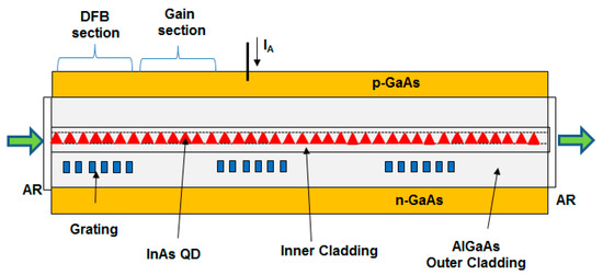
Figure 1.
Schematic of sample-grating quantum-dot-distributed Bragg semiconductor optical amplifier.
By splitting the length of the device (L) into equal uniform sections, the spatial-step size is equal to where and is the number of subsections. Each subsection will be labeled by = 1, 2, ···, . With the help of the transfer-matrix method, one can write the solution of the coupled-mode equations as:
The matrix is given by [2]:
where
and
The parameter is given by
where is the initial detuning, is the linewidth enhancement factor, is the internal loss of the structure, and is the material gain in the subsection . This includes the spatial dependence of the material gain.
In a separate-confinement heterostructure that has inner- and outer-cladding layers and a QD active layer, the energy-band diagram of the device consists of multiple energy states in the conduction and the valence bands. Experimental data have shown that 1.3 µm InAs/GaAs QD exhibits three energy states in the conduction band and eight energy states in the valence band plus a wetting layer state [11,12]. The separations of the electron and hole energy states are 60 and 10 meV, respectively. For simplicity, k = 0 denotes the ground state, k = 1 denotes the next higher energy state, and k = w denotes the wetting layer state. The energy diagram in the conduction band is shown in Figure 2.
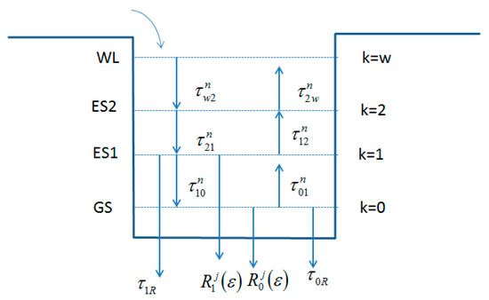
Figure 2.
Energy-band diagram of the conduction band of the device.
Carriers injected to the active layer see and interact with the QD energy states and their dynamics are described by the rate equations. Carrier transport between the dot states is determined by capture/escape rates, spontaneous-emission rate, and stimulated-emission rate. The rate equation for electrons in the k-th energy state for subsection will be written as [15]:
where and are, respectively, the occupation probability for the electrons and holes in the k-th state, and is the spontaneous radiative lifetime in k-th state. The electron capture rate is given by
The electron emission rate is
where is the electron capture lifetime and is the electron escape lifetime. in Equation (8) is the stimulation emission rate, which is given by
where is the dot-volume density and is the material gain coefficient of the QD layer, which is a Gaussian function and is function of the transition-matrix elements. For the ground state (k = 0), the second term in the right-hand side of Equation (8) is equal to . While for the wetting layer state (k = w), the first term in the right-hand side of Equation (8) is equal to , where is the normalized applied current. Similar-rate equations can be written for the hole states. The relation between the electron and the hole concentration is governed by the charge-neutrality equation, which is given by
where is the volume density of the k-th state, and are the electron and the hole concentration of the wetting layer, and and are the number of electron and hole states, respectively. The modal gain of the active layer is
where is the material gain coefficient of the active layer which is given by [15]:
where is the inhomogeneous line broadening, is the maximum gain coefficient for the k–kp transition, is the photon energy of the amplifier, is the energy corresponding to the gain peak of the k–kp transition, and C is a constant extracted from the transition-matrix elements, which takes into account the selection rule and homogeneous line broadening [16]. In the following analysis, the homogeneous line broadening is not included since the bandwidth of the device is extremely narrow.
3. Results and Discussions
The device consists of 3 periods of sample-grating DFB and gain sections as shown in Figure 1. The length of the DFB section is 100 µm and the length of the gain section is 470 µm. For 3 periods, the total length of the device is 1710 µm. The device parameters, obtained from the literature, are given in Table 1 [15,16,17]. The Bragg wavelength is chosen to be equal to the QD ground-state wavelength and the device operates at 0.98 of the threshold conditions. To include the spatial dependence of the gain, the device is divided into segments, the rate equations are simultaneously solved in each section, and the boundary conditions are applied. The input–output characteristics of the device are evaluated in a reverse manner to resolve the device nonlinearity (i.e., the inputs are evaluated when the output is known). The procedure is as follows: the output powers for the two signals is varied by running two do loops (one for the data output and the other for the control output) and the corresponding inputs are evaluated. The input powers are saved in two matrices. The outputs that correspond to fixed inputs are then extracted. In the following analysis, we define the wavelength shift as the shift between the input wavelength and the Bragg wavelength i.e., . The input power of the control and data signals is denoted by and , respectively.

Table 1.
Parameters used for the investigated device.
The optical-transmission spectrum of the device displays multiple peaks corresponding to the multiple modes of the sample-grating structure. The optical gain of the device for single input, i.e., no XGM, is shown in the inset of Figure 3. The first 3 dual modes are shown and labeled by , , and in the inset of Figure 3. As evident, the optical-gain spectrum exhibits comb peaks separated by = 1.5 Å between closely adjacent modes like and , and = 4.8 Å between next adjacent modes like and . The unsaturated optical gain is about 50 dB. For input power equal to 10 µW, the comb peaks vary between 17 dB to 18 dB, and, for higher input power, the multiple channels show approximately equal response. Figure 3 shows a zoom in for the optical spectrum for mode and for 8 µW and 20 µW input power. As shown, the peak of mode is 0.3 dB higher gain than mode for = 20 µW, and this gain variation reduces when increases. As evident, increasing the input power () shifts the mode spectrum to higher wavelength. For example, when the input power is very small compared with the input saturation power, mode is peaked at 0.2 Å (i.e., the mode unsaturated wavelength shift is 0.2 Å). When = 20 µW, the wavelength shift that corresponds to the mode peak is increased to 0.4 Å. According to Figure 3, the device modes exhibit spectral bistability at the higher-wavelength side of each mode spectrum. Clockwise spectral hysteresis loops are obtained at specific wavelengths for all comb modes. When increases, the optical gain peak decreases and the spectral hysteresis width increases as well. Operating the device at the wavelengths that correspond to the bistable regions will be useful for multichannel optical switching. We expect that enhanced bistable characteristics will be obtained when cross-gain modulation is presented.
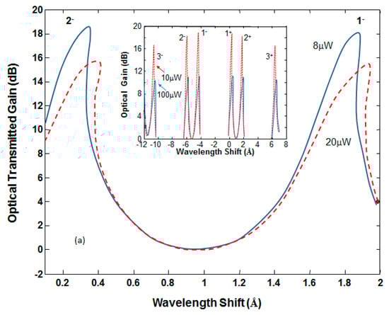
Figure 3.
Optical-transmission gain as a function of wavelength shift for single-input signal. The inset shows a wider spectral range for input power equal to 8 µW and 20 µW.
In the following analysis, the bistable characteristics of the device, governed by cross-gain modulation, are studied when multiple input signals are coupled to the comb modes. The data signal is detuned to mode and has its input power fixed at = 8 µW. The control signal, which has an input power of = 20 µW, is detuned to the other comb modes as shown in Figure 4. In Figure 4, we detuned the data wavelength to = 0.36 Å, which places mode at the upper wavelength edge of its bistable region when = 0. The optical gain of the control signal as a function of its wavelength shift is shown in Figure 4. The figure shows the control spectrum for modes and only. According to Figure 4 and as a result of XGM, the data signal significantly modifies the bistable characteristics of the control signal. When = 0 (i.e., without XGM), the control bistability region is located at the upper wavelength side of each mode, as shown by the solid line in Figure 4, and when = 8 µW (i.e., with XGM), the control signal exhibits two wider regions of bistabilities; one is located at the upper wavelength side and the other is located at the lower wavelength side, as shown by the dash line in Figure 4. This is attributed to an overlap between the control- and data-bistability regions and due to coupling between the control and data signals. Under the effect of XGM, we find that the bistability characteristics of mode are different from those of mode . In the following analysis, we will show that the bistable characteristics of mode are approximately similar to those of mode . This is attributed to the fact that modes and , which are separated by one spectral period, exhibit approximately similar spectral gain and similar power dependence. The optical gain of the data signal is shown in Figure 5 as a function of . As evident, the optical gain of the data signal as well as its bistable regions can be controlled by detuning ; detuning to mode and is only shown in the figure. We find that detuning the control wavelength to mode provides different hysteresis width and shape compared with mode . Modes that have similar power dependence exhibit similar bistable characteristics. According to Figure 5, 16 dB contrast ratio can be obtained by operating the device at = −4.1 Å or −5.6 Å.
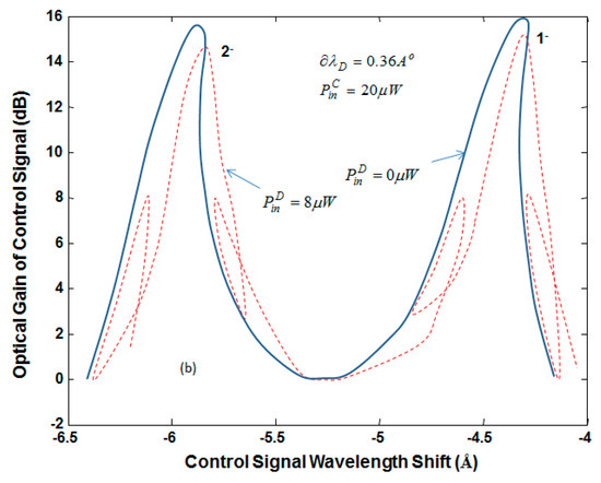
Figure 4.
Optical gain of control signal as a function of control wavelength shift at fixed input powers.
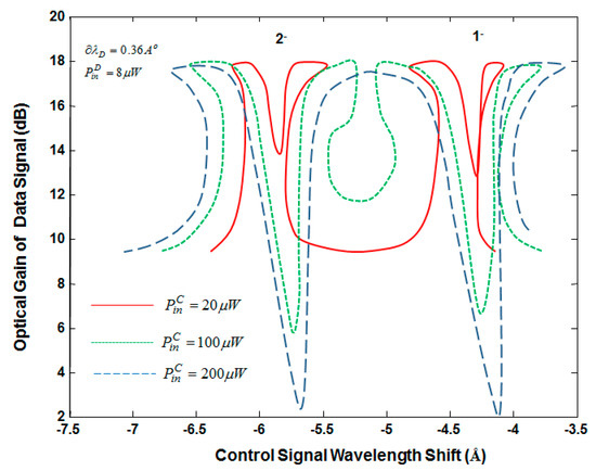
Figure 5.
Optical gain of data signal as a function of control-wavelength shift at fixed input.
The shape of the spectral bistability, as well as the hysteresis width, can be adjusted by changing input parameters. The optical gain of the data signal is shown in Figure 5 as a function of for different control-input power (). A dip in the data gain, which occurred at = −4.1 Å or −5.6 Å when is increased, was due to gain saturation caused by large control gain. The dip split the mode into two regions; upper bistable region and lower bistable region for < 100 µW. This feature was obtained when the control and data wavelengths are properly detuned by 0.4 Å and 0.16 Å above the mode unsaturated wavelength. According to Figure 5, the upper bistable region of all modes is shifted to higher wavelength and the lower bistable region is shifted to lower wavelength when is increased. When reaches 200 µW or more, the lower wavelength side of mode and the upper wavelength side of mode merges and becomes stable. According to Figure 4 and Figure 5, bistability is limited to a narrow wavelength range.
The hysteresis width and shape are power-dependent. This phenomenon can be utilized to get multiple optical bistability if the control and data inputs are properly tuned to the comb modes. The power multistable characteristics for = +0.36 Å are shown in Figure 6, when the control wavelength is tuned to modes , , and , i.e., is tuned to −5.6 Å, −4.1 Å, +2.15 Å and +6.77 Å. This corresponds to 0.4 Å wavelength shift above the modes’ unsaturated wavelengths. The data response may be classified into 3 states: the 9 dB state, the ~18 dB state, and the ~1 dB state. The three states are surrounded by bistability regions (with wide hysteresis widths) that increase the noise margin between these states. The three states are useful for setting and resetting all-optical flip-flops built using this device. The characteristics of the device when the control wavelength is tuned to mode and look very similar since these modes approximately exhibit similar power dependence. A three-state logic gate can be implemented from the output of the data signal. Figure 6 indicates that multichannel control inputs can be used to adjust the gain and bistability of another data channel. This feature is very attractive for building all-optical logic gates and flip-flops. Figure 7 shows the characteristics of the device when the control wavelength is tuned to mode (i.e., = −4.1 Å) and data wavelength is detuned to different comb modes (i.e., the data wavelength is tuned by 0.16 Å above the mode unsaturated wavelength). As evidence, one control channel can be used to adjacent the bistability of multiple data channels. The tristability is also limited to a very narrow wavelength range, which can be considered as the main drawback of the switch.
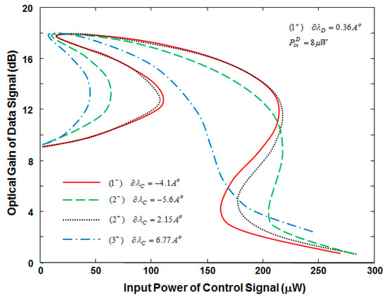
Figure 6.
Optical gain of data signal as a function of control-signal input power when the control-signal wavelength is tuned to different comb modes.
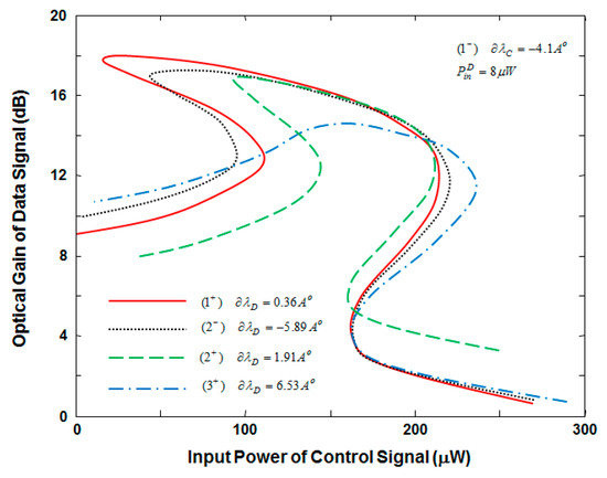
Figure 7.
Optical gain of data signal as a function of control-signal input power when the control signal wavelength is fixed and the data-signal wavelength is tuned to different comb modes.
4. Conclusions
A novel type of all-optical switch using a single sample-grating quantum-dot-distributed Bragg semiconductor optical amplifier is proposed. Cross-gain modulation is utilized to switch the state of a data signal by one or more control channels. It has been shown that multistability of a data channel can be adjusted by multichannel control inputs when the input signals are properly tuned to the sample-grating comb modes. Switching between three logic states with a contrast ratio of 8 dB and 18 dB has been demonstrated. A relatively wide noise margin/ hysteresis width between the logic states is obtained. The device characteristics are very useful for building all-optical logic gates, flip-flops, and design circuits.
Funding
This research received no external funding.
Acknowledgments
Part of the open-access fees is paid by the deanship of research at Jordan University of Science and Technology.
Conflicts of Interest
The authors declare no conflict of interest.
References
- Huang, Z.; Cao, T.; Chen, L.; Yu, Y.; Zhang, X. Monolithic Integrated Chip with SOA and Tunable DI for Multichannel All-Optical Signal Processing. IEEE Photonics J. 2018, 10, 1–9. [Google Scholar] [CrossRef]
- Qasaimeh, O. All-optical multistability using cross-gain modulation in quantum-dot distributed feedback semiconductor optical amplifier. Opt. Quantum Electron. 2018, 50, 1–9. [Google Scholar] [CrossRef]
- Huybrechts, K.; D’Oosterlinck, W.; Morthier, G.; Baets, R. Proposal for an All-Optical Flip-Flop Using a Single Distributed Feedback Laser Diode. IEEE Photonics Technol. Lett. 2008, 20, 18–20. [Google Scholar] [CrossRef]
- Dhoore, S.; Li, L.; Abbasi, A.; Roelkens, G.; Morthier, G. Demonstration of a Discretely Tunable III-V-on-Silicon Sampled Grating DFB Laser. IEEE Photonics Technol. Lett. 2016, 28, 2343–2346. [Google Scholar] [CrossRef]
- Akrout, A.; Dridi, K.; Abdul-Majid, S.; Seregelyi, J.; Hall, T.J. Numerical Study of Dual Mode Generation Using a Sampled-Grating High-Order Quantum-Dot Based Laterally-Coupled DFB Laser. IEEE J. Quantum Electron. 2013, 49, 821–828. [Google Scholar] [CrossRef]
- Liu, S.; Shi, Y.; Hao, L.; Xiao, R.; Chen, X. Experimental Demonstration of the Anti-Symmetric Sampled Bragg Grating. IEEE Photonics Technol. Lett. 2017, 29, 353–356. [Google Scholar] [CrossRef]
- Li, L.; Shi, Y.; Zhang, Y.; Zou, H.; Shen, J.; Chen, X. Study on a DFB Laser Diode Based on Sampled Grating Technique for Suppression of the Zeroth Order Resonance. IEEE Photonics J. 2017, 9, 1–9. [Google Scholar] [CrossRef]
- Happach, M.; Felipe, D.; Friedhoff, V.; Kleinert, M.; Zawadzki, C.; Rehbein, W.; Brinker, W.; Möhrle, M.; Keil, N.; Hofmann, W.; et al. Temperature-Tolerant Wavelength-Setting and -Stabilization in a Polymer-Based Tunable DBR Laser. J. Lightwave Technol. 2017, 35, 1797–1802. [Google Scholar] [CrossRef]
- Vagionas, C.; Fitsios, D.; Vyrsokinos, K.; Kanellos, G.; Miliou, A.; Pleros, N. XPM- and XGM-Based Optical RAM Memories: Frequency and Time Domain Theoretical Analysis. IEEE J. Quantum Electron. 2014, 50, 683–689. [Google Scholar] [CrossRef]
- Hurtado, A.; Raghunathan, R.; Henning, I.; Adams, M.; Lester, L. Simultaneous Microwave- and Millimeter-Wave Signal Generation With a 1310-nm Quantum-Dot-Distributed Feedback Laser. IEEE J. Sel. Top. Quantum Electron. 2015, 21, 1801207. [Google Scholar] [CrossRef]
- Ababneh, J.; Qasaimeh, O. Simple model for quantum-dot semiconductor optical amplifiers using artificial neural networks. IEEE Trans. Electron Devices 2006, 53, 1543–1550. [Google Scholar] [CrossRef]
- Qasaimeh, O. Linewidth Enhancement Factor of Quantum Dot Lasers. Opt. Quantum Electron. 2005, 37, 495–507. [Google Scholar] [CrossRef]
- Loose, A.; Goswami, B.; Wünsche, H.; Henneberger, F. Tristability of a semiconductor laser due to time delayed optical feedback. Phys. Rev. E 2009, 79, 036211. [Google Scholar] [CrossRef] [PubMed]
- Zhang, Q.; Qin, C.; Chen, K.; Xiong, M.; Zhang, X. Novel optical multibistability and multistability characteristics of coupled active microrings. IEEE J. Quantum Electron. 2013, 49, 365–374. [Google Scholar] [CrossRef]
- Qasaimeh, O. Novel closed-form solution for spin-polarization in quantum dot VCSEL. Opt. Commun. 2015, 350, 83–89. [Google Scholar] [CrossRef]
- Gioannini, M.; Montrosset, I. Numerical analysis of the frequency chirp in quantum-dot semiconductor lasers. IEEE J. Quantum Electron. 2007, 43, 941–949. [Google Scholar] [CrossRef]
- Tatebayashi, J.; Ishida, M.; Hatori, N.; Ebe, H.; Sudou, H.; Kuramata, A.; Sugawara, M.; Arakawa, Y. Lasing at 1.28 /spl mu/m of InAs-GaAs quantum dots with AlGaAs cladding layer grown by metal-organic chemical vapor deposition. IEEE J. Sel. Top. Quantum Electron. 2005, 11, 1027–1034. [Google Scholar] [CrossRef]
© 2018 by the author. Licensee MDPI, Basel, Switzerland. This article is an open access article distributed under the terms and conditions of the Creative Commons Attribution (CC BY) license (http://creativecommons.org/licenses/by/4.0/).