Abstract
After demonstrating, in previous works, the proof of concept of adaptive rectifiers with active load modulation to operate simultaneously for short/long range RF Wireless Power Transfer (WPT) while maintaining a high Power Conversion Efficiency (PCE), the authors introduced in this paper a power link budget of the proposed adaptive rectifier with a compromise between distance and efficiency. Then, to further exhibit its capabilities and enhance its performance, this paper first introduced a discussion about the parameters preventing the rectifier from operating over a wide range of input powers was performed. Furthermore, active load modulation was implemented and its co-simulation results presented. Finally, an adaptive rectifier was fabricated and its results successfully compared to measured data. It exhibits 40% of PCE over a wide dynamic input range of incident RF power levels from −6 to 25 dBm at the 900 MHz in the Industrial Scientific Medical band (ISM band), with a maximum PCE of 66% for an input power of 15 dBm. The proposed devices are therefore suitable for WPT applications to harvest energy from a controlled source.
1. Introduction
Nowadays, Wireless Power Transfer (WPT) and energy scavenging have been attracting researchers and industry due to the ever-growing need for flexible, sustainable, and unfailing sources of energy. In addition, with recent advances in wireless sensor networks (WSN), e.g., the Internet of Things (IoT), such intelligent systems are further highlighting this necessity [1,2]. The aim of wireless power transfer is to allow devices to operate for an extended period of time without having to charge/replace their batteries, a critical issue because of the inherent costs and difficulties of reaching inaccessible areas. Furthermore, WPT is seen as an environmental solution and a cost-effective approach since it drastically reduces the need to recycle dead batteries [2]. WPT techniques can be classified into two main classes: (i) inductive and magnetic resonant coupling methods to transfer power over short distances (a few centimeters); and (ii) RF electromagnetic techniques utilized to transport the energy over long distances (a few meters) [3,4]. RF electromagnetic techniques are considered in this work due to their benefits in powering portable devices over longer distances.
In order to estimate the power levels that can be transmitted, received, and harvested as well as the maximum distance that can be reached, a power link budget is essential. The common method to calculate the capability of power transmission is the power link. The propagation in the free space between a transmitter and a receiver can be expressed via the well-known Friis equation where the received power available to the rectifier can be estimated as in (1)
where is the signal wavelength. () and () state, respectively, the transmitted and received power and gain of antennas separated by a distance R.
In the following calculations, we used the Federal Communication Commission (FCC) regulations with a maximum transmitting power of 30 dBm and an Effective Isotropic Radiated Power (EIRP) of 36 dBm at the UHF ISM band. Therefore, the applied transmitted power was set as 23 dBm and the gains of the transmitted and received antennas were set as 6 dBi and 2 dBi, respectively. Table 1 summarizes the received power link budget of the proposed adaptive rectifier and trade-off between distance and efficiency. Note that the system using the concept of an adaptive rectifier reaches an efficiency greater than 40% for distances up to 2 m and 49% of efficiency at 1 m.

Table 1.
RF system power link budget.
WPT through an electromagnetic technique has been applied in a diverse range of applications and fields, such as Radio Frequency Identification (RFID) [5], Wireless Sensor Networks (WSN), Wearable and Implantable Medical Devices (WIMD) [6], Structural Health Monitoring (SHM) [7], and the Internet of Things (IoT) [8]. Such applications can involve a wide range of power levels depending on the targeted applications and the distance from the controlled source: RFID (μW to mW), bio-implants (mW to W), wirelessly charging systems for user electronic devices (a few W). Consequently, the WPT process is accomplished through a rectenna, which mostly contains an antenna, a rectifier, a matching network, and an output load as illustrated in Figure 1. Once the RF wave is received by the receiving antenna, it will be converted to direct current (DC) voltage to either directly power devices or store the energy in batteries [3].
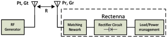
Figure 1.
Diagram illustration of Wireless Power Transfer (WPT) concept [4]. Reproduced with permission from [4], Copyright IEEE, 2016.
Several approaches have been explored to improve the efficiency of WPT systems. The rectifier is one of the most widely used sub-circuits in a WPT system to optimize its performance for maximum Power Conversion Efficiency (PCE). Numerous rectifier configurations have been suggested to improve system efficiency, including conventional configurations, such as series/shunt diodes configurations, voltage doublers, and bridge diode rectifiers [4].
However, all these topologies have noticeable limitations, such as the inability to attain a high efficiency over a wide range of input powers. This is mainly due to restrictions in diode properties, including the incapability for a diode to exhibit a low threshold voltage and a high breakdown voltage simultaneously, resulting in a degradation in power efficiency in RF–DC conversion [4]. The effect of breakdown voltage, identified as early breakdown voltage [9] can be, in fact, one of the significant issues affecting the rectifier’s efficiency.
Therefore, some approaches have been proposed to obtain a rectifier capable of handling a wide dynamic range of input power levels while exhibiting high Power Conversion Efficiency (PCE). In [1,2], the concept of a resistance compression network (RCN) has been introduced to improve the overall rectifier efficiency by attaining a small discrepancy of the input impedance while varying the output load and input power level, thus reducing the sensitivity of the input impedance rectifier versus the input power level and output load. However, the targeted input power range is still narrow. In [3,10], a rectifier with a tunable configuration has been proposed to work over a wide dynamic input power range but at the cost of a complex and bulky design where different rectifiers operating at different power level capabilities are combined in a single-pole four-throw RF switch structure. In [9,11], a topology utilizing a series diode associated with a pseudomorphic High-Electron-Mobility Transistor (pHEMT) transistor has been suggested to extend the breakdown voltage. However, such a configuration needs to be improved to cover wider input power levels. Also, maximum power point tracking (MPPT) approaches have been utilized to expand and enhance the overall conversion efficiency of the rectifier [12,13]. In [14], a nonlinear model has been proposed to rectify and recycle the harmonics with the aim of increasing the RF–DC power conversion efficiency. Moreover, an automatic load control has been proposed in [15] to improve the PCE by changing the load according to the input power variation. Furthermore, a rectifier array has been presented to extend the range of the rectification process as in [16]. Also, to extend the power range of the rectifier, an asymmetric power divider has been proposed in [17].
So, to efficiently address the issues of low efficiency and narrow input power dynamic range in conventional rectifiers, an adaptive/reconfigurable rectifier technique has been proposed to simultaneously exhibit a low threshold voltage and a high breakdown voltage [4,18]. Then, to extend its voltage breakdown, an active load modulation block [19] was added to the adaptive rectifier [20]. From that, after introducing the proof of concept of the adaptive rectifier with active load modulation in the above previous works [4,20], and to further demonstrate its capabilities and enhance its performance, this paper first introduces a power link budget of the proposed adaptive rectifier as well as an estimation of a compromise between distance and efficiency. Then, a discussion about the parameters preventing the rectifier to operate over a wide range of input powers is performed through the active device I-V characteristics and the circuit Power Conversion Efficiency. Furthermore, the active load modulation is implemented and its co-simulation results presented. Finally, an adaptive rectifier was fabricated and its results successfully compared to measured data. The adaptive rectifier concept was therefore used to extend the power input range of RF WPT systems operating at 915 MHz in the ISM band for Short/Long range WPT applications from controlled sources. This enhancement allows the RF WPT system through an electromagnetic technique to operate with true spatial freedom and be insensitive to range and location.
2. Rectifier Analysis
While used as energy harvesters, the most important characteristics of power rectifiers can be summarized below.
2.1. Efficiency
The RF–DC power conversion efficiency (PCE) is an important figure of merit to characterize and estimate a rectifier’s performance (Figure 2). It is defined as the ratio between the output DC power over the rectifier input RF power [1]
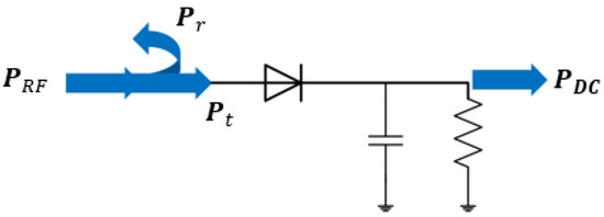
Figure 2.
Illustration of the concept of efficiency. Here PRF and Pr state the input radio frequency power and input reflected power, respectively.
is the output DC voltage across the load resistance .
2.2. Output Load
The rectifier is an alternating current (AC)/DC converter circuit. The output voltage will drive the load for specified applications, such as charging batteries or connecting it directly to electronic devices. Consequently, the output load or load resistance plays a critical role in the overall performance. As seen in (2), the load resistance, , highly affects the overall PCE and output voltage. Therefore, an optimal value of should be determined to assure maximum power conversion efficiency.
2.3. Sensitivity
In WPT and harvesting energy systems, sensitivity is a key factor in designing rectifiers. It is utilized to define the Minimum Desirable Signal (MDS) that a rectifier can deal with.
With the aim of capturing low input power levels, the rectifier components should show a low threshold voltage to attain high sensitivity [9,18].
3. Rectifier Efficiency Limitations
Designing a rectifier with high efficiency and that operates over extensive dynamic input power levels is essential for harvesting energy and wireless power transfer systems. In fact, the rectifier circuits have a diversity of factors affecting the rectifier efficiency performance while attaining a wide range of input power levels, such as active device parasitics, low breakdown voltage, high threshold voltage, nonlinear effects, mismatched impedances, and sub-optimum output load [21]. As a result, a system with optimal PCE would require a thorough set of trade-offs among these parameters. Therefore, to understand the rectifier operation and the efficiency limitations, these parameters and their impact on the circuit performance need to be investigated. In fact, the parameters effecting the rectifier to be operated over a wide range of input powers are mainly the threshold voltage, and the voltage breakdown, [21,22].
However, note that the threshold voltage, which can be defined as the voltage value from where the diode can operate and detect the input signal, is controlled by the saturation current. Consequently, having a diode with a high saturation current is desirable in WPT and harvesting energy to attain and sense low signals. Therefore, the effect of the saturation current on the overall PCE is illustrated as in Figure 3, which shows that the loss at low input power is due to the lower saturation current and vice-versa.
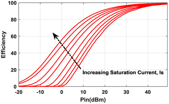
Figure 3.
Saturation current effect on the overall Power Conversion Efficiency (PCE).
On the other hand, when the rectifier device is driven by a reverse bias, the electric field near the junction can reach its maximum allowable value. Once a breakdown occurs, the current will suddenly increase while the DC output voltage remains almost constant. Therefore, voltage breakdown leads to significant efficiency degradation and attaining a rectifier with a high breakdown voltage is required to achieve high efficiency [21,23]. As noticed in Figure 4, as the voltage breakdown increases, the overall efficiency becomes broader and able to handle a wider input power range, thus achieving higher efficiency.
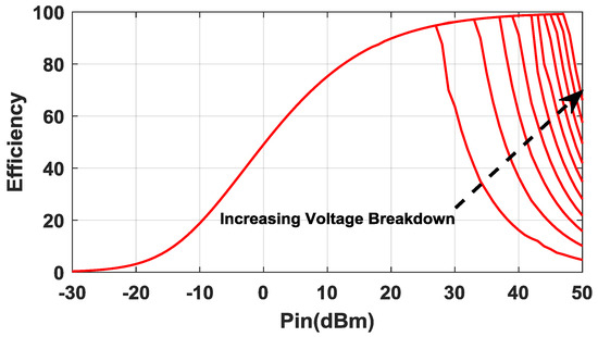
Figure 4.
Voltage breakdown effect on the overall PCE.
For this aim, a matching circuit should be taken into account to minimize mismatch loss between the antenna and the rectifier as highlighted in Figure 1. In WPT and harvesting energy circuits, designing a matching network will be more challenging since the input impedance of the rectifier needs to be matched for a particular frequency operation while its input impedance varies with the input power level [21].
Furthermore, since the diode is a nonlinear component, generating harmonics at the output can reduce the overall rectifier efficiency. In addition, the load resistance is an important parameter to consider as well; as the output load changes, the output voltage varies as well as the overall PCE. Accordingly, an optimal output load should be applied [21].
4. Design Methodology
In WPT, the usual technique to design a rectifier begins by selecting the appropriate active device, typically a diode. Based on their bias techniques, rectifier diodes can be classified into two main clusters, namely zero-biased diode configurations and non-zero-biased configurations [22]. Non-zero-biased configurations require an external source to operate, which is not appropriate in harvesting energy and wireless power transfer applications. Among the zero-bias diodes, P-N junction and Schottky barrier devices are the most widely used.
A comparison of their I-V characteristics (Figure 5) shows that the Schottky diode can turn ON at lower voltages (0.1 V–0.4 V) than can the P-N junction (e.g., 0.7 V for silicon). In addition, Schottky barrier diodes have faster switching capabilities and a much higher saturation current [22,23]. Therefore, the Schottky barrier diode is suitable for wireless power transfer and harvesting energy systems.
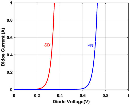
Figure 5.
I-V characteristics of P-N junction (pn) and Schottky barrier diodes (SB).
There are several commercially available Schottky diodes that can be used for a rectification process at the desired frequency operation (915 MHz), such as the HSMS-28xx family series and the SMS-76xx series [21,24], which can handle different input power levels. The HSMS2850 diode can work at low levels of input powers, i.e., less than 0 dBm (with a turn-on voltage of 150 mV and a breakdown voltage of 3.8 V), whereas the HSMS2860 diode is aimed at operating at higher levels of input powers, i.e., 0 to 20 dBm (with a turn-on voltage of 350 mV and a breakdown voltage of 7 V) [3].
When the diode device operates as a rectifier, the maximum output DC voltage is restricted by the voltage breakdown, , and can be expressed as [21]
Note that, due to output DC signal saturation, the input AC signal amplitude is limited. Therefore, the diode breakdown voltage determines the maximum peak voltage of the input waveform. As stated in [21], for a given load RL, the maximum output DC power is determined by
5. Adaptive Rectifier Design for Short/Long Range
Since a single diode cannot cover a wide input power range because of voltage breakdown limitations in the semiconductor properties, diodes with a low threshold voltage and a high breakdown voltage can be combined to achieve a rectifier operating over a wide range of input powers. The proposed rectifier, shown in Figure 6, contains three shunt Schottky diodes (D1 to D3) and a Field-Effect Transistor(FET) T1 (NE3210S1) [4], which aims at the rectifier working as a switch amongst low and high input powers. The operation procedure of the adaptive/reconfigurable rectifier can be explained as follows: once the input power level is low, the gate-source voltage across the transistor is close to zero, thus turning the transistor ON and allowing the current to pass through the channel, hence short-circuiting D2 and D3. In this case, the current pathway passes through T1 and D1. Once the input power rises, the transistor is turned OFF and D2 and D3 are working with D1. Therefore, by carefully selecting the proper diodes to operate at low and high input power levels, a low threshold voltage and a high breakdown voltage can be achieved [4,10].
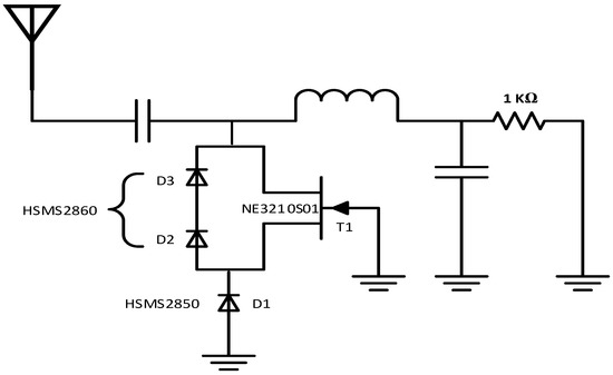
Figure 6.
Adaptive rectifier configuration [4]. Reproduced with permission from [4], Copyright IEEE, 2016.
At low input power,
and the output voltage can be expressed as in (8)
As the power increases, the voltage increases and
The outline of the adaptive rectifier concept can be illustrated through the I-V diode characteristics and Power Conversion Efficiency. As seen in Figure 7a,b, stacking two or three diodes will increase the breakdown voltage; however, the threshold voltage will increase as well. Therefore, by applying the configuration of the adaptive system in Figure 6c, a low threshold and high breakdown can be accomplished, which leads the rectifier to achieve a high efficiency while operating over wide range of input powers as can be seen in Figure 6d,e.
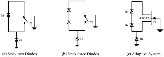
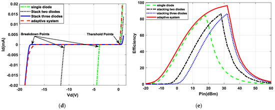
Figure 7.
Adaptive rectifier technique compared to a conventional diode rectifier, (a) Stacking two diodes, (b) Stacking three diodes, (c) Adaptive system, (d) I-V curves, (e) Power Conversion Efficiency.
6. Active Load Modulation for Simultaneous Short/Long Range WPT
To further enhance the ability of adaptive/reconfigurable rectifiers to operate over a wide input power range, an active load modulation has been applied to actively modulate and vary the output load as in Figure 8. Because the output DC power is mainly dependent on the voltage breakdown and the output load, the rectifier output load is indeed one of the crucial parameters that can affect the overall power efficiency [4,9]. Accordingly, the total PCE can be studied as a function of the load impedance (Figure 9). Here, the concept of active load modulation can be explored using active components, such as transistors, that can adjust the circuit load to increase and enhance the circuitry efficiency of a predefined input power range.
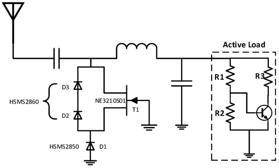
Figure 8.
Illustration of the adaptive rectifier configuration with the active load technique.
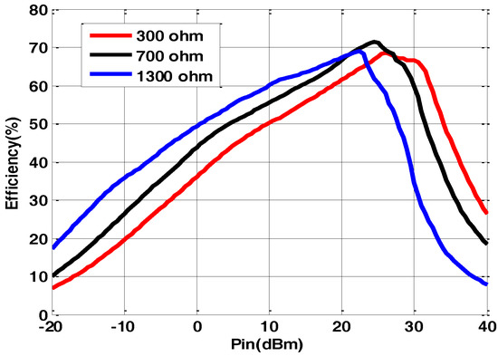
Figure 9.
Sweeping the adaptive rectifier loads versus input power level.
The design keys of having active load modulation are (i) to achieve a high voltage at a low input power to maximize the efficiency and (ii) to reduce the output voltage at a high input power to prevent the rectifier from reaching its breakdown voltage. Therefore, at low input powers, a large output load is desirable to produce a high output voltage and thus to increase the overall PCE. Once the input power increases, it is appropriate to minimize the output load to avoid the rectifier reaching its voltage breakdown, thus maintaining high PCE over a wide range of input power levels [15].
The proposed active load block, illustrated in Figure 10a, contains three resistors (R1, R2, and R3) and a switching transistor. The transistor is utilized to modify and adjust the load impedances amongst low and high input powers. For low power levels, the transistor is in the OFF-state. Consequently, the output load corresponding to impedance, as depicted in Figure 10b, is
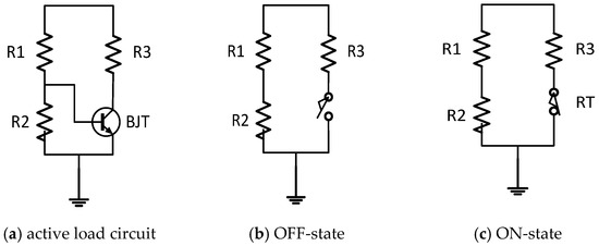
Figure 10.
Operation simplification of the active load equivalent circuit configuration: (a) active load circuit, (b) OFF-state, (c) ON-state.
As the input power rises, the transistor changes to an ON-state situation as shown in Figure 10c. Thus, the output load corresponding to impedance is then
Note that at high driving voltages, the transistor equivalent resistance (RT) can be neglected compared to R3, leading to a simplified load equivalent impedance expression as in (12).
Therefore, by applying active load modulation, a high and low load impedance can be achieved to produce a high output voltage at low power and prevent the rectifier from reaching its voltage breakdown at a high input power, thus maintaining high PCE over a wide range of input power levels.
7. Experimental Validation of the Adaptive RF WPT Harvester
Operating in the ISM band at 915 MHz, the designed adaptive rectifier (without the active load modulation technique) was optimized to operate for maximum power conversion efficiency over a wide range of RF input power levels. Simulated in Keysight’s Advanced Design System simulator [22], it uses a 31-mm-thick Rogers 5880 substrate and two transistor design kits (NE3210S1 and NE68133) from the Renesas Electronic Active Device Library. Also, the diode SPICE models (for HSMS2850 and HSMS2860) were extracted from Avago Technologies datasheets [20]. The S-parameters of the passive components (capacitors, inductors, and resistors) were taken from the datasheets provided in [23].
The fabricated adaptive rectifier circuit (Figure 11) attained a co-simulated maximum power conversion (PCE) of 66% at 15 dBm input power as depicted in Figure 12. Furthermore, it exhibits 40% of PCE over a wide dynamic input range of incident RF power levels from −6 to 25 dBm. Also, the co-simulated results are in good agreement with the measured data. However, due to equipment and test bench limitations, only measurements up to 15 dBm were performed. The rectifier achieved 4 V with an input power of 15 dBm.
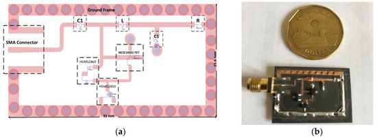
Figure 11.
Adaptive rectifier circuit: (a) co-simulation layout view (without the active load modulation block); (b) the rectifier’s printed circuit board.
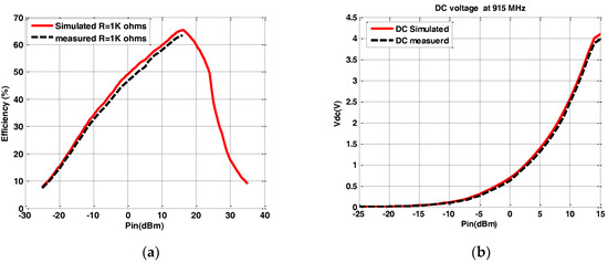
Figure 12.
Simulated and measured parameters at 915 MHz for the designed adaptive rectifier with RL = 1 kΩ: (a) Efficiency at 915 MHz; (b) output direct current (DC) voltage at 915 MHz.
Figure 13 shows the adaptive rectifier with the active load modulation block as well as a comparison of the expected PCE while using active load modulation versus fixed load values. As expected, by including the active load, the circuit presents a higher co-simulated efficiency, over 40%, and within a wider range of RF input power levels (−7 dBm to 32 dBm) compared to fixed loads. The active load resistors were adjusted to attain maximum efficiency over the desired wide range of input power levels (R1 = 1 kΩ and R2 = R3 = 0.3 kΩ). Therefore, the load varies from 0.3 kΩ to 1.3 kΩ. A low pass filter, L, and C2 were added to the rectifier circuit. Since the real part is almost constant in the Smith chart, the series capacitor (C1) is enough to match the rectifier circuit to the antenna input (50 Ω). The adaptive active load modulation achieved a DC output voltage of around 3.25 V at the input power of 15 dBm. The reconfigurable rectifier consumes an area of 30 × 17 mm2.
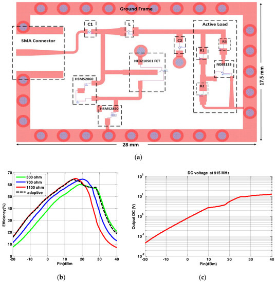
Figure 13.
Adaptive rectifier circuit with an active load configuration: (a) Co-simulation layout view; (b) Efficiency with active load and fixed passive load values; and (c) output DC voltage at 915 MHz.
To conclude, as reported in Table 2, the proposed rectifier performance was demonstrated through a successful comparison with existing published designs. The proposed designs demonstrated an extensive range of input power levels to address the issue of conventional rectifiers by simultaneously utilizing the adaptive reconfigurable configuration along with the active load modulation approach.
Table 2.
Rectifier Performance Comparison.
8. Conclusions
In this work, an adaptive rectifier concept was implemented to address the early breakdown voltage issue of conventional rectifiers while exhibiting high efficiency over a wide range of RF input power levels. The proposed rectifier achieved an efficiency of over 40% of the RF input power level ranging from −6 to 25 dBm and accomplished 66% of maximum peak power efficiency at 15 dBm. To further improve the adaptive rectifier efficiency, an active load impedance block was added to expand the efficiency of the adaptive rectifier’s performance. The results from the active load modulation topology demonstrated a 40% RF-DC power conversion efficiency over a wider range of input power levels (−6 dBm to 32 dBm) while keeping the maximum peak power efficiency at 66% at 15 dBm. The rectifier circuit was designed to extend the power input range of RF WPT Harvesters operating at 915 MHz in the ISM band for Short/Long range WPT applications from controlled sources to operate with true spatial freedom and be insensitive to range and location.
Author Contributions
Conceptualization, A.M.A.; Methodology, A.M.A., R.E.A., J.A.L., and M.C.E.Y.; Supervision, R.E.A. and M.C.E.Y.; Validation, A.M.A., R.E.A., J.A.L., and M.C.E.Y.; Writing (review & editing), A.M.A., R.E.A., and M.C.E.Y.
Funding
This research received no external funding.
Acknowledgments
The authors would like to express their thanks to the Saudi Cultural Bureau in Ottawa for their support. They would also like to thank Eqab Almajali and M. A. Le Hénaff, from the School of Electrical Engineering and Computer Science, University of Ottawa, for their help in PCB fabrication.
Conflicts of Interest
The authors declare no conflict of interest.
References
- Niotaki, K.; Georgiadis, A.; Collado, A.; Vardakas, J.S. Dual-band resistance compression networks for improved rectifier performance. IEEE Trans. Microw. Theory Tech. 2014, 62, 3512–3521. [Google Scholar] [CrossRef]
- Nintanavongsa, P.; Muncuk, U.; Lewis, D.R.; Chowdhury, K.R. Design optimization and implementation for RF energy harvesting circuits. IEEE J. Emerg. Sel. Top. Circuits Syst. 2012, 2, 24–33. [Google Scholar] [CrossRef]
- Marian, V.; Allard, B.; Vollaire, C.; Verdier, J. Strategy for microwave energy harvesting from ambient field or a feeding source. IEEE Trans. Power Electron. 2012, 27, 4481–4491. [Google Scholar] [CrossRef]
- Almohaimeed, A.M.; Yagoub, M.C.E.; Amaya, R.E. A highly efficient power harvester with wide dynamic input power range for 900 MHz wireless power transfer applications. In Proceedings of the 16th Mediterranean Microwave Symposium, Abu Dhabi, UAE, 14–16 November 2016; pp. 1–4. [Google Scholar]
- Hong, S.S.B.; Ibrahim, R.; Khir, M.H.M.; Daud, H.; Zakariya, M.A. Rectenna architecture based energy harvester for low power RFID application. In Proceedings of the International Conference on Intelligent and Advanced Systems, Kuala Lumpur, Malaysia, 12–14 June 2012; pp. 382–387. [Google Scholar]
- Deshmukh, S.D.; Shilaskar, S.N. Wearable sensors and patient monitoring system: A review. In Proceedings of the International Conference on Pervasive Computing, St-Louis, MI, USA, 23–27 March 2015; pp. 1–3. [Google Scholar]
- Park, G.; Rosing, T.; Todd, M.D.; Farrar, C.R.; Hodgkiss, W. Energy harvesting for structural health monitoring sensor networks. J. Infrastruct. Syst. 2008, 14, 64–79. [Google Scholar] [CrossRef]
- Costanzo, A.; Masotti, D. Wirelessly powering: An enabling technology for zero-power sensors, loT and D2D communication. In Proceedings of the MTT-S International Microwave Symposium, Phoenix, AZ, USA, 17–22 May 2015; pp. 1–4. [Google Scholar]
- Liu, Z.; Zhong, Z.; Guo, Y.X. Enhanced dual-band ambient RF energy harvesting with ultra-wide power range. IEEE Microw. Wirel. Compon. Lett. 2015, 25, 630–632. [Google Scholar] [CrossRef]
- Marian, V.; Vollaire, C.; Verdier, J.; Allard, B. Potentials of an adaptive rectenna circuit. IEEE Antennas Wirel. Propag. Lett. 2011, 10, 1393–1396. [Google Scholar] [CrossRef]
- Sun, H.C.; Zhong, Z.; Guo, Y.X. Design of rectifier with extended operating input power range. Electron. Lett. 2013, 49, 1175–1176. [Google Scholar] [CrossRef]
- Dolgov, A.; Zane, R.; Popovic, Z. Power management system for online low power RF energy harvesting optimization. IEEE Trans. Circuits Syst. I Regul. Pap. 2010, 57, 1802–1811. [Google Scholar] [CrossRef]
- Huang, Y.; Shinohara, N.; Mitani, T. A study on low power rectenna using DC-DC converter to track maximum power point. In Proceedings of the 2013 Asia-Pacific Microwave Conference Proceedings (APMC), Seoul, Korea, 5–8 November 2013; pp. 83–85. [Google Scholar]
- Ladan, S.; Wu, K. Nonlinear modeling and harmonic recycling of millimeter-wave rectifier circuit. IEEE Trans. Microw. Theory Tech. 2015, 63, 937–944. [Google Scholar] [CrossRef]
- Guo, J.; Hong, H.; Zhu, X. Automatic load control for highly efficient microwave rectifiers. In Proceedings of the 2012 IEEE MTT-S International Microwave Workshop Series on Innovative Wireless Power Transmission: Technologies, Systems, and Applications, Kyoto, Japan, 10–11 May 2012; pp. 171–174. [Google Scholar]
- Wang, X.; Abdelatty, O.; Mortazawi, A. Design of a wide dynamic range rectifier array with an adaptive power distribution technique. In Proceedings of the 2016 46th European Microwave Conference (EuMC), London, UK, 4–6 October 2016; pp. 922–925. [Google Scholar]
- Hamano, K.; Tanaka, R.; Yoshida, S.; Sakaki, H.; Nishikawa, K.; Kawasaki, S.; Kawai, K.; Okazaki, H.; Narahashi, S.; Shinohara, N. Wide dynamic range rectifier circuit with sequential power delivery technique. In Proceedings of the 2017 12th European Microwave Integrated Circuits Conference (EuMIC), Nuremberg, Germany, 8–10 October 2017; pp. 1155–1158. [Google Scholar]
- Sun, H.; Zhong, Z.; Guo, Y. An adaptive reconfigurable rectifier for wireless power transmission. IEEE Microw. Wirel. Compon. Lett. 2013, 23, 492–494. [Google Scholar] [CrossRef]
- Qin, Y.; Werner, D.H. Rectenna with non-linear adaptive load capable of operating over a broad range of input power levels. In Proceedings of the 2016 IEEE International Symposium on Antennas and Propagation (APSURSI), Fajardo, Puerto Rico, 26 June–1 July 2016; pp. 2155–2156. [Google Scholar]
- Almohaimeed, A.M.; Yagoub, M.C.E.; Amaya, R.E. Efficient harvester with active load modulation and wide dynamic input power range for wireless power transfer applications. In Proceedings of the 2017 Annual IEEE International Systems Conference (SysCon), Montreal, QC, Canada, 24–27 April 2017; pp. 498–501. [Google Scholar]
- Marian, V.; Allard, B.; Vollaire, C.; Verdier, J. Harvesting wireless power: Survey of energy-harvester conversion efficiency in far-field, wireless power transfer systems. IEEE Microw. Mag. 2014, 15, 108–120. [Google Scholar]
- Hemour, S.; Zhao, Y.; Lorenz, C.H.P.; Houssameddine, D.; Gui, Y.; Hu, C.M.; Wu, K. Towards low-power high-efficiency RF and microwave energy harvesting. IEEE Trans. Microw. Theory Tech. 2014, 62, 965–976. [Google Scholar] [CrossRef]
- Jaeger, R.C.; Blalock, T. Microelectronic Circuit Design, 4th ed.; McGraw-Hill Inc.: New York, NY, USA, 2011. [Google Scholar]
- Avago Technologies. Laser & Optoelectronics Progress; Avago Technologies: San Jose, CA, USA, 2009; Volume 46, p. 10. [Google Scholar]
- Wang, D.; Negra, R. Design of a dual-band rectifier for wireless power transmission. In Proceedings of the 2013 IEEE Wireless Power Transfer (WPT), Perugia, Italy, 15–16 May 2013; pp. 127–130. [Google Scholar]
- Sun, H.; Guo, Y.; He, M.; Zhong, Z. Design of a high-hfficiency 2.45-GHz rectenna for low-input-power energy harvesting. IEEE Antennas Wirel. Propag. Lett. 2012, 11, 929–932. [Google Scholar]
- Olgun, U.; Chen, C.; Volakis, J.L. Investigation of rectenna array configurations for enhanced RF power harvesting. IEEE Antennas Wirel. Propag. Lett. 2011, 10, 262–265. [Google Scholar] [CrossRef]
© 2018 by the authors. Licensee MDPI, Basel, Switzerland. This article is an open access article distributed under the terms and conditions of the Creative Commons Attribution (CC BY) license (http://creativecommons.org/licenses/by/4.0/).