Abstract
Silicon Carbide (SiC)-based Bi-Directional Switches (BDS) have great potential in the construction of several power electronic circuits including multi-level converters, solid-state breakers, matrix converters, HERIC (high efficient and reliable inverter concept) photovoltaic grid-connected inverters and so on. In this paper, two issues with the application of SiC-based BDSs, namely, unwanted turn-on and parasitic oscillation, are deeply investigated. To eliminate unwanted turn-on, it is proposed to add a capacitor (CX) paralleled at the signal input port of the driver IC (integrated circuit) and the capacitance range of CX is also analytically derived to guide the selection of CX. To mitigate parasitic oscillation, a combinational method, which combines a snubber capacitor (CJ) paralleled with the JFET (Junction Field Effect Transistor) and a ferrite ring connected in series with the power line, is proposed. It is verified that the use of CJ mainly improves the turn-off transient and the use of a ferrite ring damps the current oscillation during the turn-on transient significantly. The effects of the proposed methods have been demonstrated by theoretical analysis and verified by experimental results.
1. Introduction
Wide Band-Gap (WBG) power devices, which provide a system-level performance benefit with high-voltage blocking capability, high-temperature operation and high-frequency switching performance, have been employed in various power electronic converter applications [1,2,3,4]. The switching behavior of WBG devices, such as Silicon Carbide (SiC) and Gallium Nitride (GaN) FETs (Field Effect Transistors), has attracted considerable research attention. There are basically three issues concerning WBG device switching behavior currently being considered in research literature [3,4,5,6,7,8,9,10,11,12,13,14].
The first issue is phase-leg shoot-through, which has been widely investigated [5,6,7,8,9]. The shoot-through is due to the unintentionally turn-on behavior of the inactive switch in a phase leg that ought to be in the off-state [5]. This issue poses serious reliability concerns since it results in a short circuit with unsustainably high current flowing through the power devices. This behavior has different nomenclature in different literature, such as crosstalk [5], parasitic turn-on [6,7], cross-turn-on [8] and false turn-on [9].
The second issue is the Unwanted Turn-On (UTO) of a WBG device during its turn-off transient [3,4,10]. This issue has got less attention compared with the shoot-through issue. UTO is different from shoot-through. It is the unwanted turn-on of the active switch during its own turn-off transient, which may cause divergent oscillations and seriously impair the normal operation of the power electronic system [3]. However, shoot-through is caused by the unintentionally turn-on of the inactive switch in a phase leg circuit. UTO may pose a threat to the stability and reliability of the systems, so there is a tremendous need to analyze the root causes and find techniques to eliminate the UTO phenomenon. The self-sustained oscillation caused by UTO in a normally off SiC JFET switch was reported in [3,4]. The likelihood of self-sustained oscillation in relation to the gate resistance and the transconductance was investigated using the theory of a traditional linear oscillator circuit. The emphasis of this work was on providing a theoretical model to quantitatively predict the possibility of self-sustained oscillation of a designed SiC JFET switch and exploring the optimized gate resistance without causing self-sustained oscillation. However, the proposed quantitative analysis method to remove self-sustained oscillation is hard to be applied to more complex Bi-Directional Switch (BDS) circuits, in which parasitic components of the forward switch and the reverse switch interact complicatedly. Furthermore, its applicability to analyze other factors causing UTO is uncertain. The key research presented in [10] only revealed the detrimental impact of common source inductance on UTO in fast switching transient through simulation. The root causes of UTO in WBG-based BDS circuits remain unexplored.
The third issue concerning the efficient and stable operation of SiC systems is parasitic oscillation [11,12,13,14]. In some publications, parasitic oscillation is also referred to as parasitic ringing [11,12]. When SiC devices operate at high frequency field, parasitic oscillation is possibly present due to high switching speed and stray parasitic components. Active gate driving technique to limit high dv/dt and di/dt and suppress parasitic oscillation was reported in [1,11]. However, this approach increases circuit complexity in terms of sensing and control. The ringing phenomenon can also be damped by using an air-core PCB transformer, which has a properly designed secondary side circuit [12]. However the addition of the transformer increases the volume and cost of the system, which is not conducive to increase the power density. Alternatively, a snubber circuit was used to damp ringing during switching transient [13]. The work described in [13] considers divergent oscillation in a GaN-based cascode configuration. According to the authors, the divergent oscillation could be mitigated by adding a snubber capacitor across the Si MOSFET (Metal-Oxide-Semiconductor Field Effect Transistor) to compensate the mismatched capacitance. However, the proposed method cannot be applied to non-cascode configurations. A RC snubber and a suppression ferrite component are used to improve the switching behavior in [14]. However, only experimental investigations related to how the proposed methods can reduce the noise and switching losses are covered.
A lot of research attention has been paid to the switching behavior of WBG devices when they are used as a unidirectional switch. However, very little research has considered the switching performance of WBG devices when they are used in Bi-Directional Switches (BDSs) [15,16]. BDSs are able to conduct current and block voltage in two directions, which are referred to as four-quadrant switches. BDSs are the critical elements of several power electronic circuits, such as matrix converters, multi-level converters, solid-state breakers and HERIC (high efficient and reliable inverter concept) photovoltaic grid-connected inverters [15]. The performances of these power electronic circuits largely depend on the performances of the BDS. Unfortunately, the switching performances of WBG BDSs are rarely covered in the literature. Different from unidirectional switches, there are a forward switch and a reverse switch in a BDS. The interaction of parasitic components of the forward switch and the reverse switch is complicated, which makes the power flow analysis for a BDS more difficult. Therefore, the aim of this paper is to report a deep investigation into the UTO and parasitic oscillation of SiC JFET-based BDSs and to explore effective methods to suppress them. The paper is structured as follows: the configuration of the developed SiC JFET-based BDSs is covered in Section 2. Root cause analysis and the suppressing method of UTO are presented in Section 3. Parasitic oscillation damping measures are analysed in Section 4, while Section 5 discusses the relationship between UTO and parasitic oscillation. The theoretical analysis is validated by the experimental results shown in Section 6 and Section 7 concluding this paper.
2. The Developed Configuration of the SiC JFET-Based BDS
Lower specific on-resistance and higher current density normally on SiC JFETs, without gate-oxide problem, may be a better choice in many applications [17]. However, normally-on JFETs pose safety issues in many circuits during startup and/or abnormal gate driver conditions. One solution to this problem is to configure a normally on JFET into a normally off structure by connecting it with a low-voltage Si MOSFET in a cascode-light configuration [16,18].
The developed structure of the SiC JFET-based BDS based on the cascode-light configuration is shown in Figure 1. The BDS consists of two anti-serial unidirectional switches, each of which is in a cascode-light configuration composed of a high voltage normally on SiC N-JFET and a low-voltage Si P-MOSFET [16]. The configuration utilizes a p-channel MOSFET instead of the n-channel MOSFET that is used in the conventional cascode solution. This practice enables the driver to be connected to the common source point and to refer all voltages to this potential. This solution makes it easier to monolithically integrate both SiC JFET and Si MOSFET driver stages on one chip [19,20]. The clamping diodes (DC) and clamping resistors (RC) circuit branch in the cascode-light configuration shown in Figure 1 is considered as the JFET’s gate clamping circuit. It clamps the JFET gate to the MOSFET drain potential. In the case when the auxiliary power supply of the gate driver fails, the clamping circuit ensures the normally off behavior of the switch. The drain-source voltage that is building up over the off-state low-voltage MOSFET is being mirrored to the high voltage JFET gate-source voltage via the clamping circuit. When the level reaches the high voltage JFET pinch-off voltage, the high voltage JFET turns off and blocks the external power supply. RC in the clamping circuit is used to limit the current flowing through DC.
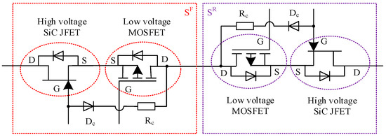
Figure 1.
The developed structure of the SiC JFET-based BDS using two anti-serial cascode-light configurations.
3. Analysis and Suppression of UTO
The switching characteristics of the developed SiC JFET-based BDS are investigated by means of a double-pulse test circuit. In order to analyze the switching transient, the transient circuit schematic diagram of the double-pulse test circuit, as shown in Figure 2, is studied.
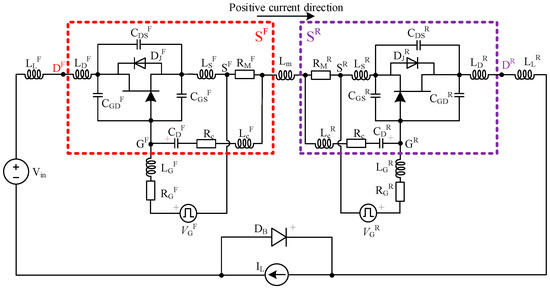
Figure 2.
The transient circuit schematic diagram of the double-pulse test circuit of SiC JFET-based BDSs.
The low-voltage MOSFETs which are always kept in on-state during normal operation are presented as resistors RMX (X = F or R) in Figure 2. The clamping diodes DC in Figure 1 are always in reverse-biased state in normal operation, thus they are replaced by their junction capacitors CDX (X = F or R) in Figure 2. For the double-pulse test, the load current can be considered constant for the duration of a switching cycle. Hence, the load inductance can be equivalent to a constant current source IL with its parasitic resistance being excluded in this paper [13,21]. In Figure 2, LYX (X = F or R; Y = L, D, G, S, C or m) means parasitic inductors. CDSX, CGDX, and CGSX (X = F or R) stand for the inter-electrode parasitic capacitors [19]. DB represents the load current freewheeling diode. Vin is a power supply in power circuit and VGX (X = F or R) represent power supplies in drive circuits.
In this paper, the positive current direction in SiC JFETs is defined as from left to right, as shown in Figure 2. The left switch serves as the forward switch (denoted as SF), while the right switch servers as the reverse switch (denoted as SR). The following transient analysis is based on the transient circuit in Figure 2.
3.1. Root Cause Analysis of UTO
In order to probe into the root cause of UTO phenomenon, the more detailed schematic diagram of the driver is exhibited in Figure 3, where VS represents the amplitude of the pulse voltage from a signal generator. RS stands for the output impedance of the signal generator. In the built double-pulse test circuit, a common signal generator is used to drive the forward switch (SF) and the reverse switch (SR) simultaneously. The driverX (X = F or R), which is represented as a transformer in Figure 3, is an isolated driver IC (Integrated Circuit) 1EDI30J12CP for normally on SiC JFETs recommended by Infineon Technologies AG [20].
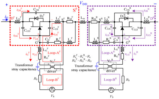
Figure 3.
Transient of the SiC JFET-based BDSs.
Once JFETs’ gate-source voltages VGSX (X = F or R) drop from 0 V to their threshold voltage Vth (around −13.5 V), turn-off transient begins and the forward switch and the reverse switch are expected to transit to their steady off-state rapidly. However, both the drain–drain voltage (VDD) and the drain current (iD) of the BDS do not mean to enter their steady state immediately. The definitions of VDD and iD are as shown in Figure 3. Oscillations are aroused due to the inherent RLC resonant network in the power loop. Very high current and voltage slew rate are resulted during the transient. According to (1), high-voltage slew rate leads to that current flows through Miller capacitance. The gate-drain capacitance CDGF under high-voltage slew rate acts as a current source charging the gate node (GF) according to (2). In (2), the shunted current in the clamping circuit is neglected due to the minute capacitance of CDF.
The voltage across the gate impedance (LGF-RGF) under such an iGF represents a positive voltage source into the gate loop (AF) according to (3). This voltage source charges the gate-source inter-electrode capacitor CGSF. The voltage across CGSF rises. When the voltage is high enough and the gate-source voltage vGSF exceeds the threshold voltage Vth, the JFET channel will be turned on. Then UTO occurs.
On the other hand, the correlation between the input and output of the driver IC is shown in Figure 4. The driver IC internal integrated Schmitt-trigger sets the driver output to high (≈0 V) when the input voltage reaches Vth-on (≈1.5 V) from a low voltage, and to low (≈−19 V) when the input voltage reaches Vth-off (≈1.4 V) from a high voltage. The practical values of Vth-on and Vth-off obtained by experiments are 1.5 V and 1.4 V, respectively, which are much lower than the specification (minimum value of Vth-on is 2.0 V; maximum value of Vth-off is 1.0 V) presented in the datasheet. Furthermore, according to the datasheet of the driver IC [20], the identifiable minimum pulse width is 40 ns determined by the internal input filter. Therefore, as long as the magnitude of the input pulse is higher than 1.5 V and the duration is longer than 40 ns, it is identified as valid drive pulses. In engineering practice, this situation might be easily triggered if the electromagnetic interference (EMI) is not well handled.
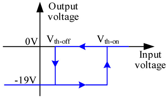
Figure 4.
Correlation between the input and output of the driver.
The electromagnetic transient in Loop-AF resonant network may interfere with the input signal in Loop-BF through stray capacitances of the internal isolating transformer. Moreover, when Vin (as defined in Figure 2) rises, the current, shunted into Loop-AF during turn-off transient, also increases and the EMI to Loop-BF becomes more serious. Once the oscillation amplitude of the input voltage in Loop-BF reaches Vth-on (≈1.5 V) and the duration is up to 40 ns [19,20], the driver IC identifies the input signal as an active trigger signal. Then active high output is set to turn on JFET. Thus UTO is triggered. When Vin is lower, the impact of EMI is smaller and the likelihood of UTO is less. When Vin is increased to 150 V for the built SiC JFET-based BDS double-pulse test circuit, in which distributed stray parameters are not finely optimized, UTO phenomenon appears, as shown in Figure 5.
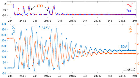
Figure 5.
UTO phenomenon during turn-off transient @Vin = 150 V.
The oscillation caused by UTO is much more serious than normal parasitic oscillation. The voltage overshoot is more than 150%, which may challenge the system safety and prevent increasing Vin.
The two unidirectional switches in the BDS are in duality. Hence, the analysis of the forward switch SF (the red part in Figure 3) in the positive current direction (from left to right) can be mapped to the reverse switch SR (the purple part in Figure 3) in the negative current direction (from right to left). Therefore, UTO analysis of reverse switch is omitted here.
3.2. UTO Suppression
From the above analysis, it can be concluded that UTO is more easily triggered by the oscillation in Loop-BF than Loop-AF owing to the lower input voltage threshold Vth-on of the driver IC. Based on this observation, a UTO suppression method is proposed by adding a filter capacitor (its capacitance is denoted by CX) close to the input pin of the driver IC, as shown in Figure 6. This filter capacitor might not be indispensable in some driver ICs while the practice proves that it is essential for the used driver IC 1EDI30J12CP.
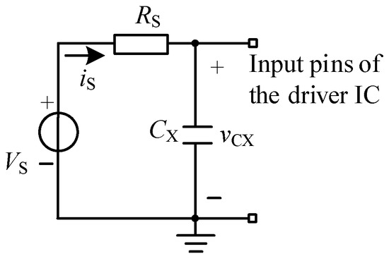
Figure 6.
CX paralleled at the signal input port of the driver IC.
In operation, high-frequency oscillation current components from the power loop (right side in Figure 6) is bypassed by CX. Consequently, the voltage across RS caused by high-frequency oscillation current components will be restrained and its impact on the input signal voltage of the drive IC will be restrained. According to (4), the bigger the capacitance CX, the smaller the shunt branch impedance and the better the filtering effect. However, the introduced delay time increases with the increase of CX and it may reduce the advantages of SiC devices in high-frequency applications. Hence, the value of CX should be properly considered.
Figure 7 shows the input signal transient waveform without paralleling CX. The turn-on delay, denoted by td-on, is approximately 20 ns and the turn-off delay, denoted by td-off, is about 27 ns. These delays are caused by undesired factors of the signal generator and the distributed stray capacitances in the circuit.
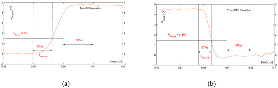
Figure 7.
Input signal of driver without CX. (a) Turn-on transient; (b) Turn-on transient.
Next, the delay introduced by paralleling CX is investigated. Without consideration the driver IC in Figure 6, (5) and (6) can be established.
where iS is as defined in Figure 6, vCX denotes the voltage drop across CX.
Then, (7) and (8) can be derived for the turn-on transient and the turn-off transient, respectively.
Thus, the turn-on delay td-on-CX and turn-off delay td-off-CX, caused by paralleling CX, can be calculated according to (9) and (10).
where Vth-on and Vth-off are the turn-on threshold voltage and the turn-off threshold voltage of the drive IC, respectively, as shown in Figure 4.
Due to the delays introduced in the signal transmission, both the time position and the width of the drive pulses are changed. Generally, the maximum acceptable delay, which impacts the switching frequency and the pulse-width accuracy, decreases with the increasing requirement of the switching speed of power devices. Here, the maximum acceptable duty cycles of the delays are discussed instead of the absolute delay values. Hence, several duty cycles are defined in (11), where ∂d-on, ∂d-off and ∂width-change are the duty cycles of the total turn-on delay, total turn-off delay and total variation of the pulse width, respectively; correspondingly, ∂d-on-max, ∂d-off-max and ∂width-change-max are the maximum acceptable duty cycles of the total turn-on delay, total turn-off delay and total variation of the pulse width, respectively; TS is the period of the PWM (Pulse-Width Modulation) control signal; td-on and td-off (defined in Figure 7) are the inherent turn-on and turn-off delay introduced by the signal generator and stray capacitors; td-on-CX and td-off-CX are the turn-on and turn-off delay purely introduced by adding CX; td-on-driver and td-off-driver are the turn-on and turn-off delays introduced by undesired factors of the drive IC [19]; td-on-JFET and td-off-JFET are the turn-on and turn-off delays introduced by undesired factors of SiC JFET devices; fS is the switching frequency.
Equation (12) can be derived by combining (9)–(11), in which min{} stands for minimum value calculation function. According to (12), the range of CX value can be calculated analytically in terms of the allowable introduced delay. Equation (12) can be used as a guideline for selecting the value of CX.
where
4. Parasitic Oscillation Suppression
High-speed switching of power devices in circuits is often accompanied by boring oscillations caused by the parasitic inductances and capacitances of the switching circuit. These boring oscillations are called parasitic oscillations. Parasitic oscillations are undesirable because they interfere with the stable operation of power electronic circuits. Also, they consume energy that decreases the system efficiency and output capacity. Furthermore, such oscillations often generate excessive voltages which might cause voltage breakdown in high-voltage applications.
In this section, two methods for suppressing parasitic oscillations in SiC JFET-based BDS are explored. One method is to add a snubber capacitor connected in parallel with JFETs in the BDS. The other method is to add a ferrite ring connected in series with the power line. The theoretical analysis of the two methods is presented in the following sections.
4.1. Effect of Adding a Snubber Capacitor on Parasitic Oscillation during Turn-Off Transient
The effect of a snubber capacitor in parallel with the JFET is analyzed in this section. Experimental results show that a snubber capacitor is more effective on the turn-off transient than on the turn-on transient. Therefore, only the turn-off transient experimental waveforms are presented in this section and the turn-on transient experimental waveforms will be given in Section 6. The typical turn-off transient waveforms without using any parasitic oscillation suppression measures are shown in Figure 8. One variation period of the parasitic oscillation can be roughly divided into two stages.
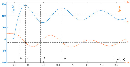
Figure 8.
Turn-off transient waveforms without using any parasitic oscillation suppression measures (Vin = 103 V, iL = 2.0 A).
4.1.1. Stage I: BDS Drain–Drain Voltage Rising
In the interval t0~t1, the drain–drain voltage VDD of the BDS is rising and the current iD is in the positive direction; the forward switch blocks the external positive voltage. VDSF is the voltages across the JFET in forward switch and VSDR is the voltages across the JFET in reverse switch. CDSF charges when the current iD is in the positive direction during the interval t0~t1, and VDSF rises. VSDR is close to 0 V because the JFET’s body diode of reverse switch is forward-biased. At the instant t1, CDSF charges to its peak value and is about to discharge; iD is around 0 A.
The transient circuit schematic diagram is shown in Figure 9 after paralleling snubber capacitors CJX (X = R or S). In the interval t0~t1, applying KCL (Kirchhoff’s Current Law) to the node DF in Figure 9, there is
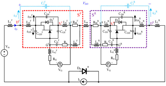
Figure 9.
Transient circuit schematic diagram when paralleling CJ.
According to (13), iDSF is subtracted by a positive value after paralleling CJF. It means that the charging current of CDSF can be decreased and the peak value of VDSF can be decreased by paralleling CJF when other conditions remain unchanged. Moreover, VDD can be expressed as
where Vstray stands for the stray voltage drop on the stay impedance between the node DF and the node DR in Figure 9.
Vstray is very small compared with Vin according to experimental measurements. Besides, with a specified iD, Vstray can be considered constant in the interval t0~t1. Furthermore, VSDR is kept close to zero during t0~t1 interval. Therefore, VDD can be decreased when VDSF is reduced according to (14). Consequently, by paralleling CJF, the peak of VDD can be reduced to some extent compared with the situation without paralleling CJF. Since low-voltage MOSFETs in the BDS are kept on-state during normal operation, snubber capacitors are paralleled with JFETs, not with the whole switch, in order to limit parasitic inductances in the snubber loop.
4.1.2. Stage II: BDS Drain–Drain Voltage Falling
In the interval t1~t2, CDSF discharges, iD turns negative and CDSR charges. Consequently, VDSF decreases from its peak and VSDR will decrease below zero. At the end of this interval, iD is about to turn positive and CDSR stops charging.
During the interval t1~t2, VDD is dropping and iD is negative; CDSF and CJF are discharged. Equation (13) is still valid under this circumstance. Therefore, by adding CJF, the current iDSF, that discharges CDSF, can be decreased. Consequently, the voltage drop amplitude can be restrained. In this way, the oscillation amplitude of VDSF gradually decays.
At instant t2, CDSF is about to charge again and another cycle begins. It can be concluded that by paralleling CJF, the peak-to-peak value of VDD can be effectively damped. The voltage oscillation during turn-off transient can be effectively suppressed.
Though adding a snubber capacitor is beneficial for the suppression of oscillation, it may reduce the system efficiency if it is not properly designed. In our test circuit, a snubber capacitor of 1.0 nF is used. At worst, the extra turn-on loss introduced by adding this snubber capacitor is 0.44 μJ, which is insignificant.
4.2. Effect of Adding a Ferrite Ring on Parasitic Oscillation during Turn-On Transient
Experimental results show that a ferrite ring connected in series with the power line is more effective on improving the turn-on transient behavior than the turn-off transient behavior. Though larger voltage overshoot will be caused during turn-off transient by adding a ferrite ring, this secondary phenomenon of ferrite ring will be neutralized by snubber capacitances CJX (X = F or R) which is verified by the experimental results in the Section 6. Therefore, the effect of a ferrite ring on the turn-on transient is only analyzed in this section.
The transient circuit schematic diagram after adding a ferrite ring is shown in Figure 10. Before adding the ferrite ring, (15) and (16) are valid.
where VZL denotes the voltage drop caused by the total parasitic impedance ZL (=RL + jω0LL) of the power line and VDB denotes the voltage drop across the diode DB. ω0 denotes the oscillation frequency.
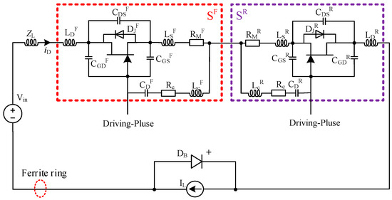
Figure 10.
Dynamic schematic circuit after adding a ferrite ring.
Equation (17) can be easily derived by combining (15) and (16)
The equivalent circuit of a ferrite ring can be considered as a series connection of frequency-dependent resistance and inductance [14]. Thus, the equivalent effect of inserting a ferrite ring can be regarded as the increase of ZL, and at the same time the damping resistance. According to (15)–(17), the increased parasitic impedance ZL and the added damping resistance are beneficial to limit the slew rate and the peak value of the current. Hence, the current oscillation during turn-on transient can be effectively damped by adding a ferrite ring.
The condition (18) should be met when selecting a ferrite ring for effective suppression of parasitic oscillation [14].
where R and XL stand for the resistance and reactance of the ferrite ring at the oscillation frequency fosc, respectively. A ferrite ring with parameters satisfying (18) gives sufficient damping. If (18) is not met, the suppression effect of the ferrite ring may not be significant.
The ferrite ring used in the experiment is measured by impedance analyzer WK6500B. The impedance frequency characteristic of the employed ferrite ring is shown in Figure 11. According to Figure 11, the effective dampening frequency range is from 0.65 MHz to 8.81 MHz, in which the condition R > XL is met. Since the impedance of the ferrite ring is very low at low frequency, the resulted power loss is insignificant at low frequency as shown in Figure 11. Furthermore, the addition of a ferrite ring can effectively suppress parasitic oscillation and decrease oscillation loss. Thus, as long as the condition (18) is met, the total losses will be reduced after applying ferrite ring [14].
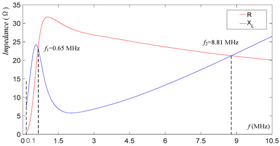
Figure 11.
Impedance frequency characteristic of the ferrite ring used for parasitic oscillations dampening.
4.3. Combined Effects of the Snubber Capacitor and the Ferrite Ring
According to the above analysis, a snubber capacitor and a ferrite ring can damp parasitic oscillations during turn-on transient and turn-off transient respectively. Hence, combining the two methods is expected to be more effective. The effects will be demonstrated by experiments in the Section 6.
5. Relationship between UTO and Parasitic Oscillation
Once UTO occurs, parasitic oscillation will be aggravated. When UTO occurs periodically in a constant cycle, undamped oscillation or even divergent oscillation may occur [3,4]. A limited number of UTO means that damped oscillations will be the result.
On the other hand, serious parasitic oscillation is accompanied by high dv/dt and di/dt, which increase the likelihood of UTO. The lower amplitude of parasitic oscillation is beneficial to the elimination of UTO. Therefore, the amplitude of parasitic oscillation should be restrained.
In summary, the capacitor CX paralleled at the driver signal input port mainly mitigates UTO, while the voltage oscillation during turn-off transient and the current oscillation during turn-on transient can be damped by combining CJ and the ferrite ring. Paralleling CX has little impact on parasitic oscillation of the power loop. Switching performance will be greatly improved by combining the three methods.
6. Experimental Result and Discussion
To validate the correctness of the theoretical analysis and effectiveness of the proposed methods, an experimental test setup has been established to carry out the double-pulse test. The schematic diagram of the setup is depicted in Figure 2. The actual experimental setup is shown in Figure 12.
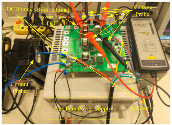
Figure 12.
Photo of the built SiC JFET-based double-pulse test setup.
One of three BDSs in a 3 × 1 SiC JFET-based matrix converter is tested. Two phases of the stator windings of a permanent magnet synchronous machine (PMSM) are used as the load with a total inductance of 11.2 mH. Such arrangement is to simulate the real application system. SiC Schottky diode IDH16G120C5 [22] is used as the freewheeling diode DB. Two high-power DC (Direct Current) programmable power supplies (GEN 300-50 from TDK Lambda AMERICAS, National City, CA, USA) connected in series are used as the DC power source. The experimental data are acquired by an oscilloscope DPO4104B (Beaverton, OR, USA), differential voltage probes TA043 (Cambridge, UK), a current probe TCP312A (Beaverton, OR, USA) and plotted by Matlab (2016a, Natick, MA, USA).
6.1. Mitigation of UTO
The two-pulse drive signal is generated by a signal generator DG1022. VS is 5 V and RS is 50 Ω according to the datasheet [23]. fS is assumed to be 50 kHz. The duty cycles of the delay time and the pulse width variation should be as small as possible. Generally, no larger than 1% is acceptable in practical applications [24,25]. Therefore, ∂d-on-max, ∂d-off-max and ∂width-change-max is set to 0.01 in the test. The other parameter values of the test circuit which are obtained from experimental results are given in Table 1.

Table 1.
Model parameters of the double-pulse test circuit.
Putting parameters in Table 1 to (12), there is
In light of (9) and (10), the smaller CX is, the smaller the delay is. Figure 13 shows the comparison of td-on-CX and td-off-CX between the experimental results and the theoretical results calculated by (9) and (10) with the variation of CX. The calculated time matches well with the experimental results over a wide range of CX. The difference is within 9 ns, which is minute.
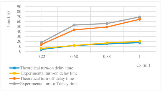
Figure 13.
Comparison of td-on-CX and td-off-CX between experimental results and calculation results.
From the point of view of the introduced signal delay, a capacitor of 0.22 nF is the best among the four capacitances, as shown in Figure 13. Then, a low-ESL (Equivalent Series Inductance) Multilayer Ceramic Capacitor (MLCC) of 0.22 nF is first tested. Experiments show that UTO occurs when Vin increases to around 227 V and IL is around 4.5 A, as indicated in Figure 14. UTO aggravates the oscillation. The peak of the voltage reaches 487 V and the peak of the load current runs up to 8.1 A in Figure 14. Periodic UTO and undamped or divergent oscillations may emerge if Vin exceeds 227 V under this set of experimental parameters. Nevertheless, by comparing Figure 14 with Figure 5, it is obvious that UTO phenomenon in BDS is significantly alleviated through utilization of CX of 0.22 nF.
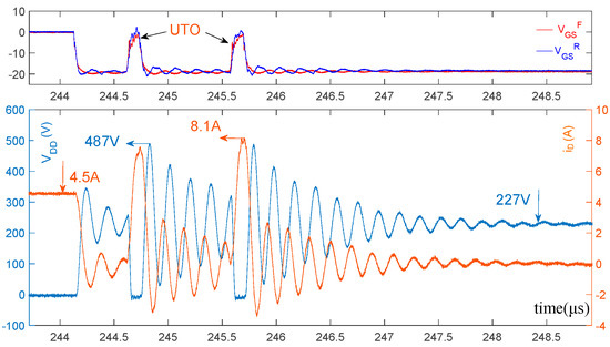
Figure 14.
Turn-off transient under the condition of Vin = 227 V, IL = 4.5 A, CX = 0.22 nF.
Taking into account the introduced delay and UTO suppression effect simultaneously, the effect of a low-ESL MLCC of 0.68 nF is tested. According to the experimental results, Vin can be increased to 550 V for the established SiC JFET-based BDS without triggering UTO, with CX being 0.68 nF. 550 V is the maximum output voltage of the DC power supply used in the built experimental setup. It is thus clear that UTO suppression effect is significant with paralleling CX. Figure 15 shows the experimental results under the condition of Vin = 300 V, IL = 6.1 A with CX = 0.68 nF. It can be seen that a voltage overshoot of 197 V is observed, which may be too large in some practical applications. One of the main reasons for the large voltage overshoot is the bigger conductor inductance in the power loop of the experimental setup, which is measured as 780 nH by the impedance analyzer WK6500B. The large conductor inductance of the power line is due to the relative long distance between the DC source and power devices, which is the case in some practical applications. The purpose of the designed experiments is to simulate the applications where the conductor has to be long. Therefore, the experiments are conducted with a 780 nH conductor inductance. A CX of 0.68 nF is used in the following experiments.
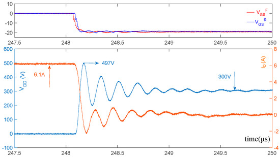
Figure 15.
Turn-off transient under the condition of Vin = 300 V, IL = 6.1 A, CX = 0.68 nF.
6.2. Impact of the Snubber Capacitor on the Turn-off Behavior
Figure 16 shows the impacts of CJ on the turn-off transient under the condition of Vin = 103 V, IL = 2.0 A, CX = 0.68 nF, CJ = 1.0 nF. In this experiment, no ferrite ring is used. Figure 16a presents the waveforms without CJ, while Figure 16b shows the waveforms with CJ. By comparing Figure 16a and Figure 16b, it can be seen that, by paralleling CJ with the JFET, the peak value of VDD is reduced by 23 V and the overshoot of VDD is reduced from 45% to 23%. The settling time of the voltage oscillation is increased a bit from 1.7 µs to 1.8 μs, which is insignificant. The loss of turn-off transient, which is calculated by experimental waveforms, is reduced from 9.2 μJ to 8.4 μJ. The resonating frequency fosc is decreased from 5.1 MHz to 4.0 MHz. Therefore, it can be concluded that the suppression effect of CJ on the turn-off parasitic oscillation is verified.
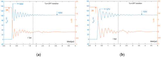
Figure 16.
Turn-off transient under the condition of Vin = 103 V, IL = 2.0 A, CX = 0.68 nF. (a) Turn-off transient without CJ; (b) Turn-off transient with CJ of 1.0 nF.
6.3. Impact of the Ferrite Ring on the Turn-On Behavior
Figure 17 shows the impacts of the ferrite ring during turn-on transient under the condition of Vin = 103 V, IL = 2.0 A. In this experiment, CJ is not paralleled. Figure 17a presents the waveforms without the ferrite ring, while Figure 17b shows the waveforms with the ferrite ring.
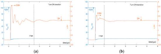
Figure 17.
Turn-on transient under the condition of Vin = 103 V, IL = 2.0 A, CX = 0.68 nF. (a) Turn-on transient without a ferrite ring; (b) Turn-on transient with a ferrite ring.
By comparing Figure 17a,b, it can be seen that the turn-on switching performance is significantly improved in the following aspects. The overshoot of iD is greatly reduced from 80% to 30%; the settling time of the current oscillation is reduced from 1.8 μs to 1.0 μs; the loss of turn-on transient calculated by experimental waveforms is reduced from 6.5 μJ to 4.1 μJ. The oscillation cycles are significantly reduced.
From the experiments, it can be summarized that the ferrite ring has excellent capability to absorb high-frequency noise and make the voltage and current waveforms cleaner. Furthermore, it is significantly smaller than the volume and weight of conventional EMI filters [14]. The specifications of the used ferrite ring are 19 mm in length, 50 mm in diameter and 125.3 g in weight. Thus, it can be concluded that the ferrite ring is a high cost-effective alternative in optimizing the SiC device turn-on waveform without causing much increase in loss, volume and weight.
6.4. Combined Effects of the Snubber Capacitor and the Ferrite Ring
Figure 16 and Figure 17 verify that a snubber capacitor and a ferrite ring can damp parasitic oscillation during turn-on transient and turn-off transient respectively. In the following experiments, CX of 0.68 nF is still used.
Figure 18 shows the switching transient waveforms without using CJ or the ferrite ring. And Figure 19 shows the switching transient waveforms with CJ of 1.0 nF and the ferrite ring. It can be seen that, after adding CJ and the ferrite ring, the overshoot of iD is reduced from 72% to 26%; the settling time of the current oscillating is reduced from 2.3 μs to 1.1 μs; the overshoot of VDD is reduced from 64% to 29%; the resonating frequency fosc during turn-off transient is reduced from 6.8 MHz to 4.4 MHz. The ferrite ring is measured to be 26 Ω and 0.34 μH at the frequency of 4.4 MHz according to Figure 11. These parameters meet the condition R > XL.
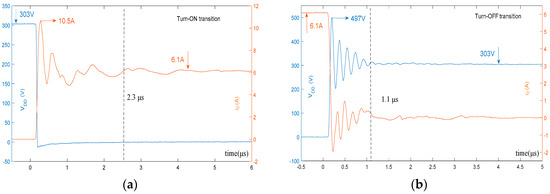
Figure 18.
Switching transient under the condition of Vin = 303 V, IL = 6.1 A, CX = 0.68 nF. (a) Turn-on transient without damping; (b) Turn-off transient without damping.
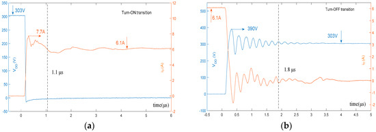
Figure 19.
Switching transient under the condition of Vin = 303 V, IL = 6.1 A, CX = 0.68 nF. (a) Turn-on transient with ferrite ring and CJ; (b) Turn-off transient with ferrite ring and CJ.
The loss of turn-on transient is reduced from 40.1 μJ to 18.5 μJ and the loss of turn-off transient is increased from 42.3 μJ to 48.6 μJ due to the prolonged settling time caused by the ferrite ring and the settling time of the voltage oscillating is increased from 1.1 µs to 1.8 μs. However, these defects could be somewhat neutralized when considering the total damping effects. The total switching loss is reduced from 82.4 μJ to 67.1 μJ with utilization of the snubber capacitor and the ferrite ring under the condition of Vin = 303 V, IL = 6.1 A, CX = 0.68 nF.
The relative experimental data are presented in Table 2. By comparing experimental data before and after taking relative measures, it can be said that the effectiveness of the proposed methods is experimentally verified.
Table 2.
Comparison of experimental data under different conditions.
7. Conclusions
UTO phenomenon in the application of high-speed SiC devices has multiple adverse effects. It may result in undamped or divergent oscillations which are detrimental to the reliable operation of power electronic circuits. This paper reports a deep investigation into the UTO behavior of a developed SiC JFET-based BDS. Detailed theoretical analysis has been conducted to probe into the root cause of UTO. In order to mitigate UTO, it has been proposed to simply add a capacitor (CX) paralleled at the signal input port of the driver IC and the value range of the capacitance of CX is derived quantitatively. Experimental results verify the effectiveness of CX on the suppression of UTO in SiC JFET-based BDSs.
Switching parasitic oscillations have negative impacts on the performance and efficiency of BDSs. In order to exploit the full potential of SiC JFET-based BDSs, proper handling methods of the parasitic oscillation have been explored. Two methods to alleviate parasitic oscillation in the SiC JFET-based BDS, namely, paralleling a snubber capacitor (CJ) with JFET and connecting a ferrite ring in series with the power line, have been deeply explored in this paper. Adoption of CJ mainly makes turn-off transient waveforms better while the ferrite ring damps the current oscillation during turn-on transient. Besides, the ferrite ring is proven to be a high cost-effective method in making the switching waveforms cleaner and less noisy. The combination of CJ and a ferrite ring can significantly damp parasitic oscillation. Detailed theoretical analysis has been presented and experimental results confirm the effectiveness of the proposed methods.
Author Contributions
L.W. and J.Y. contributed to the main idea of this article. J.Y. wrote the paper. J.Y., K.O.O. and H.M. performed the experiments and collected data. L.W., J.Y., H.M., Z.W. and K.D.E.K. contributed to analysis of data. Z.W. searched literature. L.W., H.M., Z.W., K.O.O. and K.D.E.K. revised the paper critically. All authors approved the final version to be published.
Funding
This research was funded by the National Natural Science Foundation of China grant number 51577005 and the Aeronautical Science Foundation of China grant number 2015ZC51030.
Conflicts of Interest
The authors declare no conflict of interest.
References
- Camacho, A.P.; Sala, V.; Ghorbani, H.; Martinez, J.L.R. A novel active gate driver for improving SiC MOSFET switching trajectory. IEEE Trans. Ind. Electron. 2017, 64, 9032–9042. [Google Scholar] [CrossRef]
- Liu, T.; Ning, R.; Wong, T.T.; Shen, Z.J. Modeling and analysis of SiC MOSFET switching oscillations. IEEE J. Emerg. Sel. Top. Power Electron. 2016, 4, 747–756. [Google Scholar] [CrossRef]
- Lemmon, A.; Mazzola, M.; Gafford, J.; Parker, C. Instability in half-bridge circuits switched with wide band-gap transistors. IEEE Trans. Power Electron. 2014, 29, 2380–2392. [Google Scholar] [CrossRef]
- Lemmon, A.; Mazzola, M.; Gafford, J.; Parker, C. Stability considerations for silicon carbide field-effect transistors. IEEE Trans. Power Electron. 2013, 28, 4453–4459. [Google Scholar] [CrossRef]
- Jahdi, S.; Alatise, O.; Gonzalez, J.A.O.; Bonyadi, R.; Ran, L.; Mawby, P. Temperature and switching rate dependence of crosstalk in Si-IGBT and SiC power modules. IEEE Trans. Ind. Electron. 2016, 63, 849–863. [Google Scholar] [CrossRef]
- Velander, E.; Löfgren, A.; Kretschmar, K.; Nee, H.P. Novel solutions for suppressing parasitic turn-on behaviour on lateral vertical JFETs. In Proceedings of the 16th European Conference on Power Electronics and Applications, Lappeenranta, Finland, 26–28 August 2014; pp. 1–8. [Google Scholar]
- Heer, D.; Bayerer, R.; Domes, D. SiC-JFET in half-bridge configuration-parasitic turn-on at current commutation. In Proceedings of the International Exhibition and Conference for Power Electronics, Intelligent Motion, Renewable Energy and Energy Management (PCIM), Nuremberg, Germany, 19–20 May 2014; pp. 1–8. [Google Scholar]
- Miao, Z.; Wang, C.M.; Ngo, K.D. Simulation and characterization of cross-turn-on inside a power module of paralleled SiC MOSFETs. IEEE Trans. Compon. Packag. Manuf. Technol. 2017, 7, 186–192. [Google Scholar] [CrossRef]
- Ahmed, M.R.; Todd, R.; Forsyth, A.J. Predicting SiC MOSFET behavior under hard-switching, soft-Switching, and false turn-on conditions. IEEE Trans. Ind. Electron. 2017, 64, 9001–9011. [Google Scholar] [CrossRef]
- Zhang, W.; Zhang, Z.; Wang, F.; Costinett, D.; Tolbert, L.; Blalock, B. Common source inductance introduced self-turn-on in MOSFET turn-off transient. In Proceedings of the Applied Power Electronics Conference and Exposition (APEC), Tampa, FL, USA, 26–30 March 2017; pp. 837–842. [Google Scholar]
- Nayak, P.; Hatua, K. Parasitic Inductance and capacitance-assisted active gate driving technique to minimize switching loss of SiC MOSFET. IEEE Trans. Ind. Electron. 2017, 64, 8288–8298. [Google Scholar] [CrossRef]
- Kim, J.; Shin, D.; Sul, S.K. A damping scheme for switching ringing of full SiC MOSFET by air core PCB circuit. IEEE Trans. Power Electron. 2017, 33, 4605–4615. [Google Scholar] [CrossRef]
- Huang, X.; Du, W.; Lee, F.C.; Li, Q.; Zhang, W. Avoiding divergent oscillation of a cascode GaN device under high-current turn-off condition. IEEE Trans. Power Electron. 2017, 32, 593–601. [Google Scholar] [CrossRef]
- Josifović, I.; Popović-Gerber, J.; Ferreira, J.A. Improving SiC JFET switching behavior under influence of circuit parasitics. IEEE Trans. Power Electron. 2012, 27, 3843–3854. [Google Scholar] [CrossRef]
- Saadeh, M.; Chinthavali, M.S.; Ozpineci, B.; Mantooth, H.A. Anti-series normally-On SiC JFETs operating as bidirectional switches. In Proceedings of the Energy Conversion Congress and Exposition (ECCE 2013), Denver, CO, USA, 15–19 September 2013; pp. 2892–2897. [Google Scholar]
- Wang, L.; Zhang, X.; Deng, J.; Yang, J.; Oladele, O.K.; Zhao, Y. Unwanted turn-on of SiC JFET bi-directional switches under influence of parasitic parameters. In Proceedings of the 43rd Industrial Electronics Society (IECON 2017), Beijing, China, 29–30 October 2017; pp. 4194–4199. [Google Scholar]
- Santi, E.; Peng, K.; Mantooth, H.A.; Hudgins, J.L. Modeling of wide-bandgap power semiconductor devices—Part II. IEEE Trans. Electron Devices 2015, 62, 434–442. [Google Scholar] [CrossRef]
- Siemieniec, R.; Kirchner, U. The 1200V direct-driven SiC JFET power switch. In Proceedings of the 14th European Conference on Power Electronics and Applications, Birmingham, UK, 30–31 August 2011; pp. 1–10. [Google Scholar]
- Infienon Chip, 1EDI30J12CP Single JFET Driver IC. Available online: https://www.infineon.com/cms/en/product/power/gate-driver-ics/galvanic-isolated-gate-driver/1edi30j12cp/ (accessed on 12 November 2014).
- Application Note AN2013-17 EiceDRIVER™ Enhanced 1EDI30J12Cx. Available online: https://www.infineon.com/cms/en/search.html#!view=downloads&term=EiceDRIVER%E2%84%A2#32Enhanced#321EDI30J12Cx/ (accessed on 16 December 2013).
- Huang, X.; Li, Q.; Liu, Z.; Lee, F.C. Analytical loss model of high voltage GaN HEMT in cascode configuration. IEEE Trans. Power Electron. 2014, 29, 2208–2219. [Google Scholar] [CrossRef]
- Infienon Chip, 5th Generation thinQ!™ 1200 V SiC Schottky Diode IDH16G120C5. Available online: https://www.infineon.com/cms/en/product/power/silicon-carbide-sic/coolsic-schottky-diode/idh16g120c5/ (accessed on 21 July 2017).
- RIGAL. DG1022 Double Channel Function/Arbitrary Waveform Generator. Available online: http://www.rigol.com/ (accessed on 15 January 2010).
- Fereidoony, F.; Mirtaheri, S.A.; Chamaani, S. High-resolution range estimation using time delays in ultra-wideband M-sequence radar. IET Microw. Antennas Propag. 2017, 11, 1332–1339. [Google Scholar] [CrossRef]
- Wang, Q.; Krautschneider, W.H.; Weber, W.; Schmitt-Landsiedel, D. Influence of MOSFET IV characteristics on switching delay time of CMOS inverters after hot-carriers stress. IEEE Electron Device Lett. 1991, 12, 238–240. [Google Scholar] [CrossRef]
© 2018 by the authors. Licensee MDPI, Basel, Switzerland. This article is an open access article distributed under the terms and conditions of the Creative Commons Attribution (CC BY) license (http://creativecommons.org/licenses/by/4.0/).