AlGaN/GaN MIS-HEMT with PECVD SiNx, SiON, SiO2 as Gate Dielectric and Passivation Layer


Abstract
1. Introduction
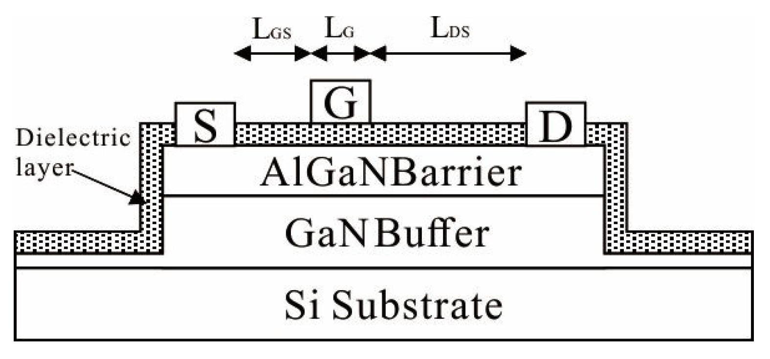
2. Materials and Methods
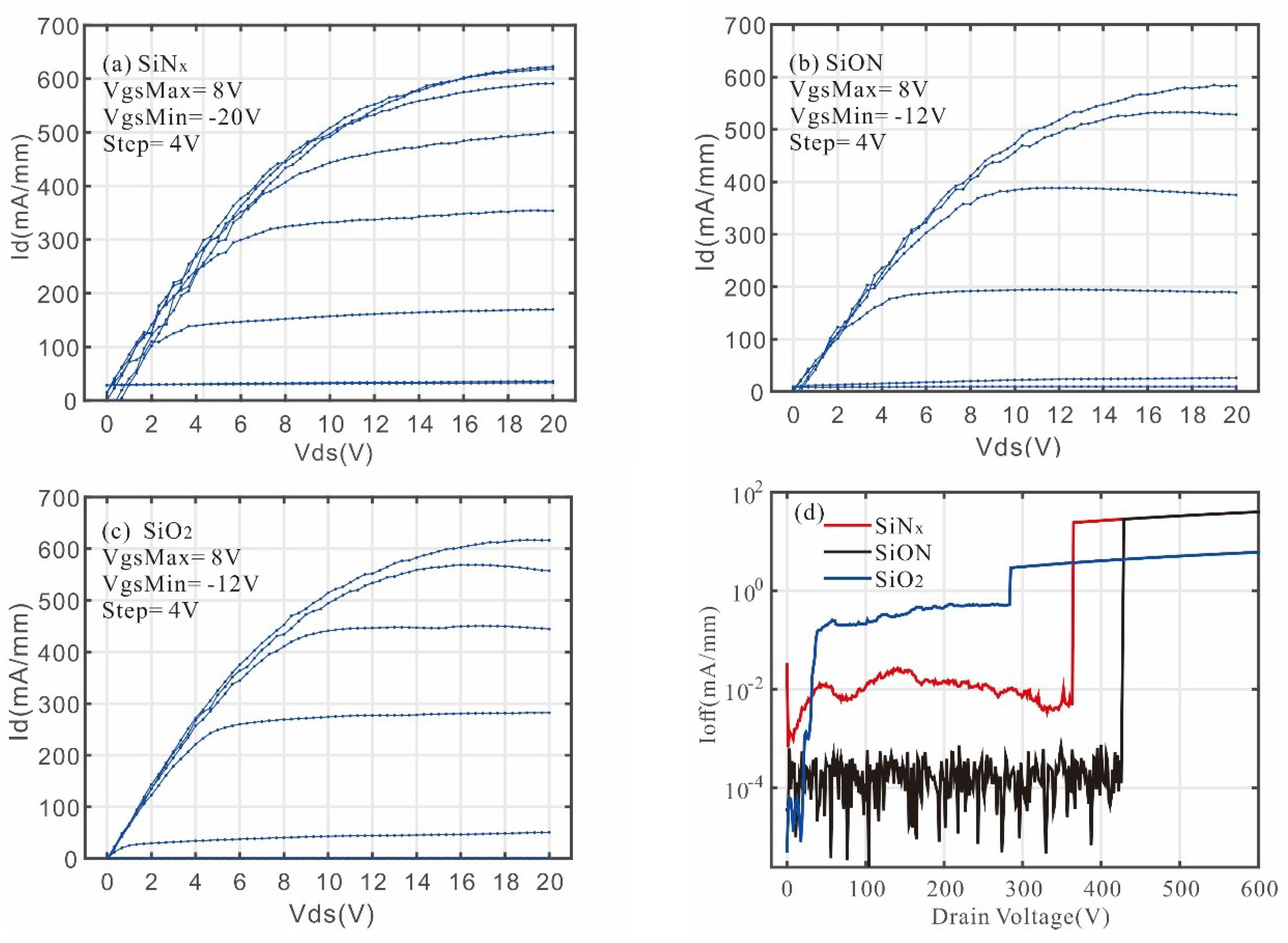
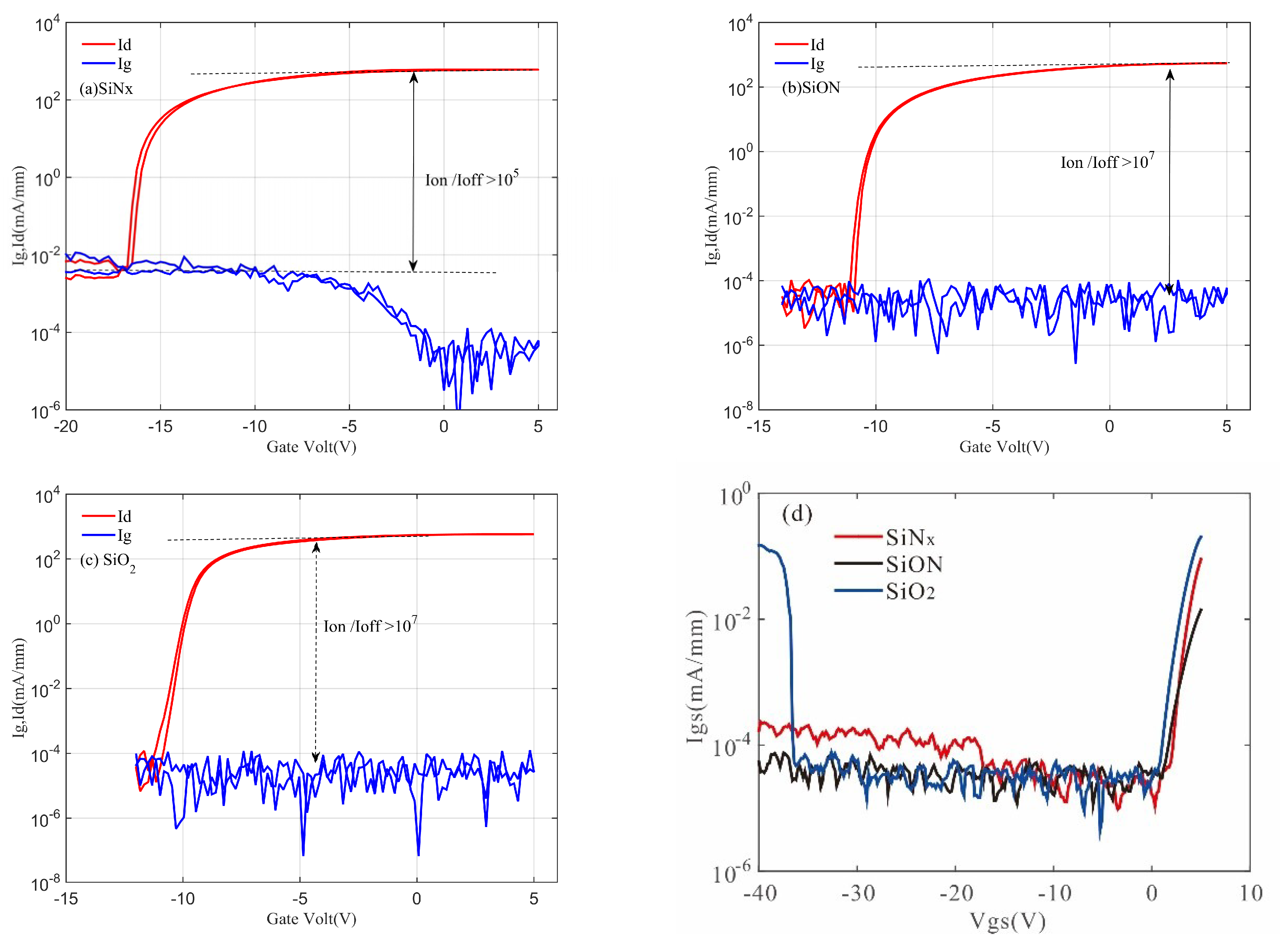
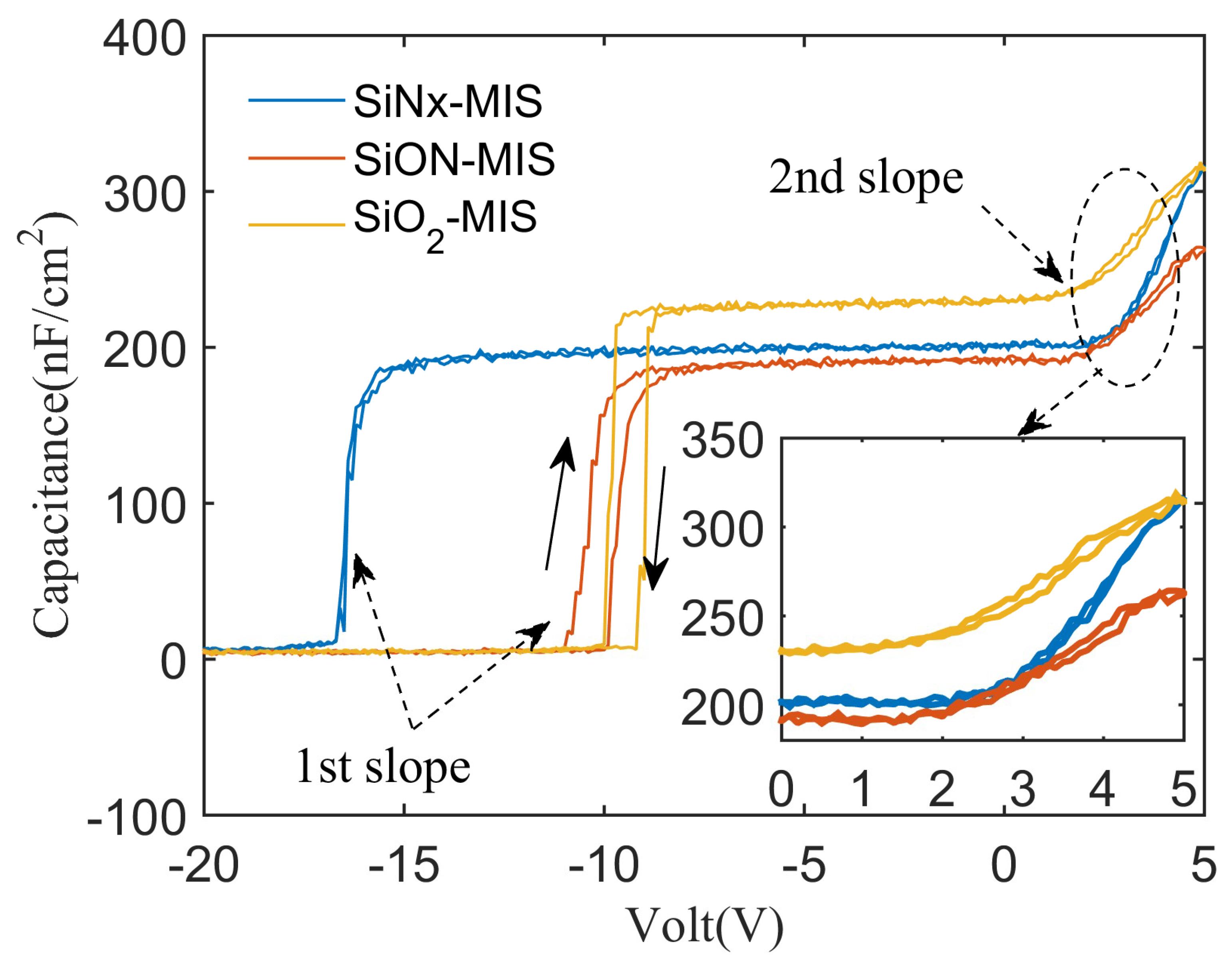
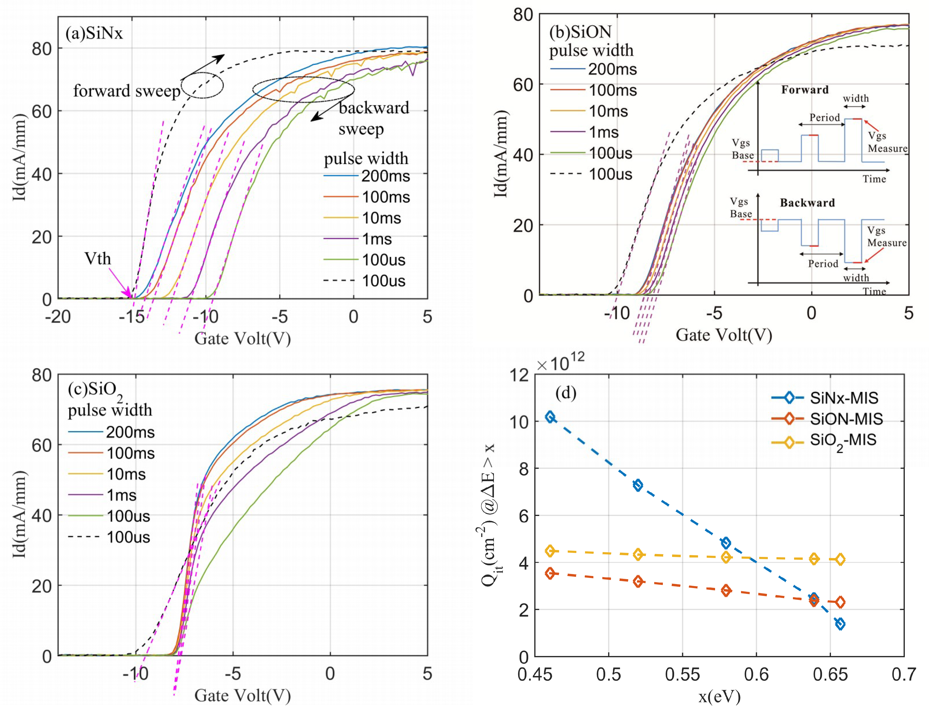
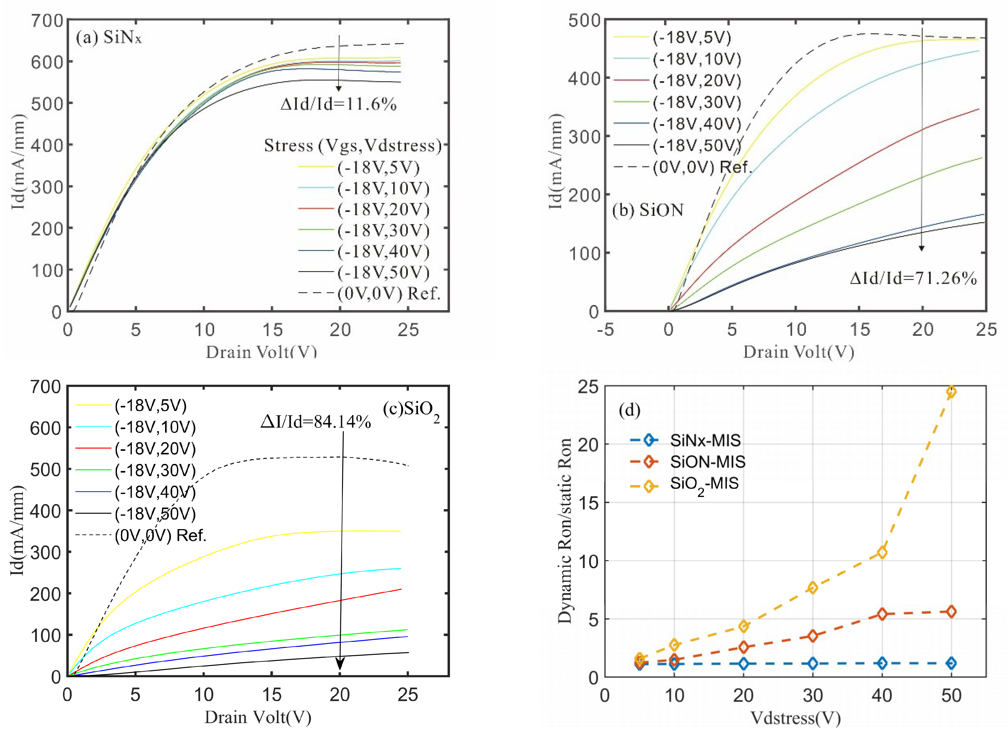
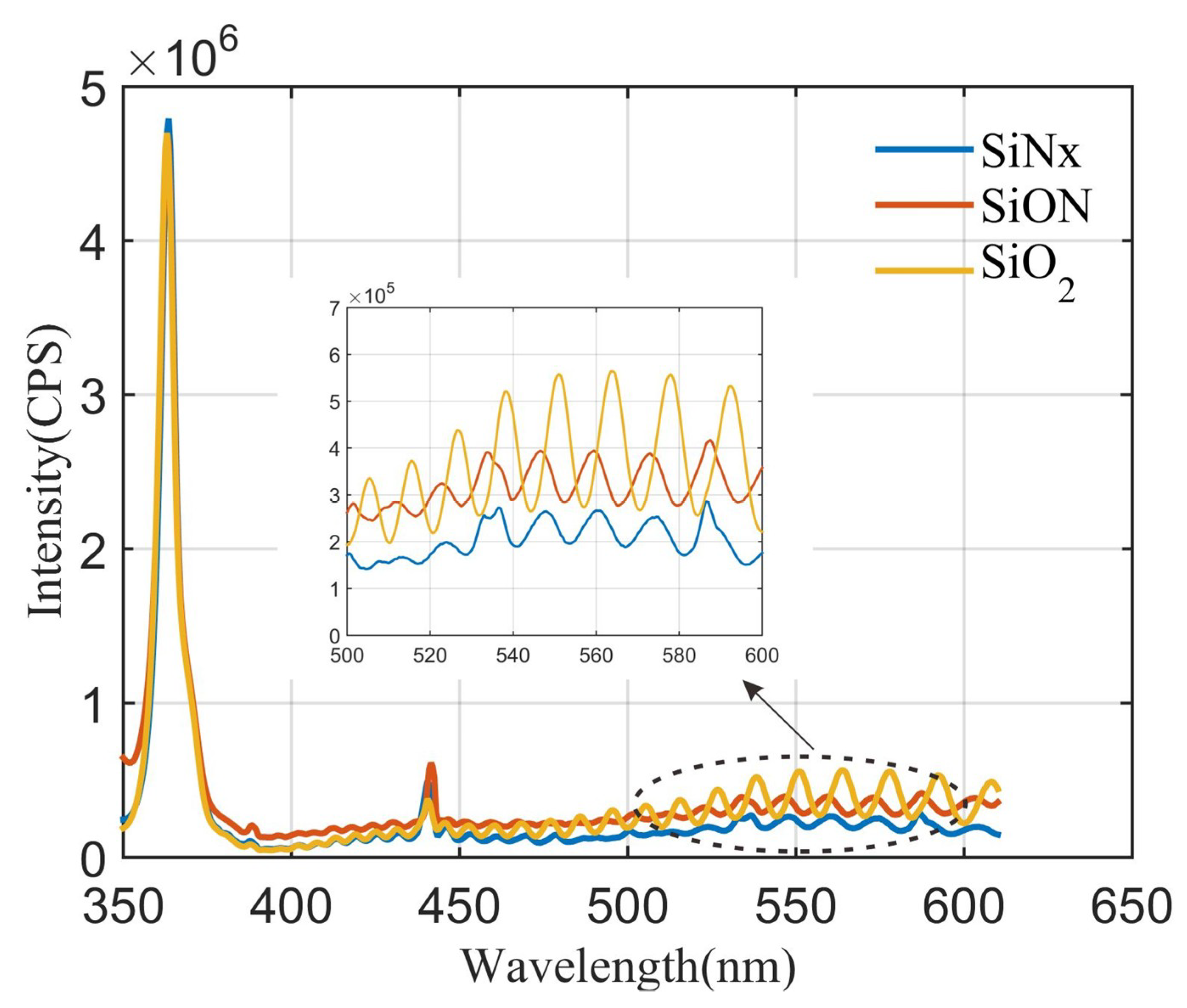
3. Results and Discussion
4. Conclusions
Author Contributions
Funding
Conflicts of Interest
References
- Chen, K.J.; Haberlen, O.; Lidow, A.; Tsai, C.L.; Ueda, T.; Uemoto, Y.; Wu, Y. GaN-on-Si Power Technology: Devices and Applications. IEEE Trans. Electron. Dev. 2017, 64, 779–795. [Google Scholar] [CrossRef]
- Lee, J.; Kim, H.; Seo, K.; Cho, C.; Cha, H. High quality PECVD SiO2 process for recessed MOS-gate of AlGaN/GaN-on-Si metal–oxide–semiconductor heterostructure field-effect transistors. Solid State Electron. 2016, 122, 32–36. [Google Scholar] [CrossRef]
- Chakroun, A.; Jaouad, A.; Soltani, A.; Arenas, O.; Aimez, V.; Ares, R.; Maher, H. AlGaN/GaN MOS-HEMT Device Fabricated Using a High Quality PECVD Passivation Process. IEEE Electr. Device Lett. 2017, 38, 779–782. [Google Scholar] [CrossRef]
- Kordoš, P.; Heidelberger, G.; Bernát, J.; Fox, A.; Marso, M.; Lüth, H. High-power SiO2/AlGaN/GaN metal-oxide-semiconductor heterostructure field-effect transistors. Appl. Phys. Lett. 2005, 87, 143501. [Google Scholar] [CrossRef]
- Arulkumaran, S.; Egawa, T.; Ishikawa, H. Studies of Electron Beam Evaporated SiO2/AlGaN/GaN Metal—Oxide—Semiconductor High-Electron-Mobility Transistors. Jpn. J. Appl. Phys. 2005, 44. [Google Scholar] [CrossRef]
- Chiou, Y. Photo-CVD SiO2 Layers on AlGaN/GaN/AlGaN MOS-HFETs. J. Electrochem. Soc. 2004, 151, G863–G865. [Google Scholar] [CrossRef]
- Jiang, H.; Liu, C.; Chen, Y.; Lu, X.; Tang, C.W.; Lau, K.M. Investigation of Insitu SiN as Gate Dielectric and Surface Passivation for GaN MISHEMTs. IEEE Trans. Electron. Dev. 2017, 64, 832–839. [Google Scholar] [CrossRef]
- Tang, Z.; Jiang, Q.; Lu, Y.; Huang, S.; Yang, S.; Tang, X.; Chen, K.J. 600-V Normally Off SiNx/AlGaN/GaN MIS-HEMT With Large Gate Swing and Low Current Collapse. IEEE Electr Device Lett. 2013, 34, 1373–1375. [Google Scholar] [CrossRef]
- Zhang, Z.; Yu, G.; Zhang, X.; Deng, X.; Li, S.; Fan, Y.; Sun, S.; Song, L.; Tan, S.; Wu, D.; et al. Studies on High-Voltage GaN-on-Si MIS-HEMTs Using LPCVD Si3N4 as Gate Dielectric and Passivation Layer. IEEE Trans. Electron. Dev. 2016, 63, 731–738. [Google Scholar] [CrossRef]
- Arulkumaran, S.; Hong, L.Z.; Ing, N.G.; Selvaraj, S.L.; Egawa, T. Influence of Ammonia in the Deposition Process of SiN on the Performance of SiN/AlGaN/GaN Metal–Insulator–Semiconductor High-Electron-Mobility Transistors on 4-in. Si(111). Appl. Phys. Express 2009, 2, 31001. [Google Scholar] [CrossRef]
- Adivarahan, V.; Gaevski, M.; Sun, W.H.; Fatima, H.; Koudymov, A.; Saygi, S.; Simin, G.; Yang, J.; Khan, M.A.; Tarakji, A.; et al. Submicron gate Si3N4/AlGaN/GaN-metal-insulator-semiconductor heterostructure field-effect transistors. IEEE Electr. Device Lett. 2003, 24, 541–543. [Google Scholar] [CrossRef]
- Kim, H.; Han, S.; Jang, W.; Cho, C.; Seo, K.; Oh, J.; Cha, H. Normally-Off GaN-on-Si MISFET Using PECVD SiON Gate Dielectric. IEEE Electr. Device Lett. 2017, 38, 1090–1093. [Google Scholar] [CrossRef]
- Balachander, K.; Arulkumaran, S.; Egawa, T.; Sano, Y.; Baskar, K. A comparison on the Electrical Characteristics of SiO2, SiON and SiN as the Gate Insulators for the Fabrication of AlGaN/GaN Metal–Oxide/Insulator–Semiconductor High-Electron Mobility-Transistors. Jpn. J. Appl. Phys. 2005, 44, 4911–4913. [Google Scholar] [CrossRef]
- Balachander, K.; Arulkumaran, S.; Egawa, T.; Sano, Y.; Baskar, K. Demonstration of AlGaN/GaN metal-oxide-semiconductor high-electron-mobility transistors with silicon-oxy-nitride as the gate insulator. Mater. Sci. Eng. B 2005, 119, 36–40. [Google Scholar] [CrossRef]
- Balachander, K.; Arulkumaran, S.; Ishikawa, H.; Baskar, K.; Egawa, T. Studies on electron beam evaporated ZrO2/AlGaN/GaN metal-oxide-semiconductor high-electron-mobility transistors. Phys. Status Solidi A 2005, 202, R16–R18. [Google Scholar] [CrossRef]
- Ye, P.D.; Yang, B.; Ng, K.K.; Bude, J.; Wilk, G.D.; Halder, S.; Hwang, J.C.M. GaN metal-oxide-semiconductor high-electron-mobility-transistor with atomic layer deposited Al2O3 as gate dielectric. Appl. Phys. Lett. 2005, 86, 63501. [Google Scholar] [CrossRef]
- Liu, Z.H.; Ng, G.I.; Arulkumaran, S.; Maung, Y.K.T.; Teo, K.L.; Foo, S.C.; Sahmuganathan, V.; Xu, T.; Lee, C.H. High Microwave-Noise Performance of AlGaN/GaN MISHEMTs on Silicon with Al2O3 Gate Insulator Grown by ALD. IEEE Electr. Device Lett. 2010, 31, 96–98. [Google Scholar]
- Asif, M.; Chen, C.; Peng, D.; Xi, W.; Zhi, J. Improved DC and RF performance of InAlAs/InGaAs InP based HEMTs using ultra-thin 15 nm ALD-Al2O3 surface passivation. Solid State Electron. 2018, 142, 36–40. [Google Scholar] [CrossRef]
- Liu, C.; Chor, E.F.; Tan, L.S. Investigations of HfO2/AlGaN/GaN metal-oxide-semiconductor high electron mobility transistors. Appl. Phys. Lett. 2006, 88, 173504. [Google Scholar] [CrossRef]
- Anand, M.J.; Ng, G.I.; Vicknesh, S.; Arulkumaran, S.; Ranjan, K. Reduction of current collapse in AlGaN/GaN MISHEMT with bilayer SiN/Al2O3 dielectric gate stack. Phys. Status Solidi C 2013, 10, 1421–1425. [Google Scholar] [CrossRef]
- Balachander, K.; Arulkumaran, S.; Sano, Y.; Egawa, T.; Baskar, K. Fabrication of AlGaN/GaN double-insulator metal-oxide-semiconductor high-electron-mobility transistors using SiO2 and SiN as gate insulators. Phys. Status Solidi A 2005, 202, R32–R34. [Google Scholar] [CrossRef]
- Miyazaki, E.; Goda, Y.; Kishimoto, S.; Mizutani, T. Comparative study of AlGaN/GaN metal-oxide-semiconductor heterostructure field-effect transistors with Al2O3 and HfO2 gate oxide. Solid State Electron. 2011, 62, 152–155. [Google Scholar] [CrossRef]
- Chang, Y.C.; Huang, M.L.; Chang, Y.H.; Lee, Y.J.; Chiu, H.C.; Kwo, J.; Hong, M. Atomic-layer-deposited Al2O3 and HfO2 on GaN: A comparative study on interfaces and electrical characteristics. Microelectron. Eng. 2011, 88, 1207–1210. [Google Scholar] [CrossRef]
- Green, B.M.; Chu, K.K.; Chumbes, E.M.; Smart, J.A.; Shealy, J.R.; Eastman, L.F. The effect of surface passivation on the microwave characteristics of undoped AlGaN/GaN HEMTs. IEEE Electr. Device Lett. 2000, 21, 268–270. [Google Scholar] [CrossRef]
- Meneghesso, G.; Verzellesi, G.; Danesin, F.; Rampazzo, F.; Zanon, F.; Tazzoli, A.; Meneghini, M.; Zanoni, E. Reliability of GaN High-Electron-Mobility Transistors: State of the Art and Perspectives. IEEE Trans. Device Mater. Reliab. 2008, 8, 332–343. [Google Scholar] [CrossRef]
- Arulkumaran, S.; Ng, G.I.; Liu, Z.H. Effect of gate-source and gate-drain Si3N4 passivation on current collapse in AlGaN/GaN high-electron-mobility transistors on silicon. Appl. Phys. Lett. 2007, 90, 173504. [Google Scholar] [CrossRef]
- Arulkumaran, S.; Egawa, T.; Ishikawa, H.; Jimbo, T.; Sano, Y. Surface passivation effects on AlGaN/GaN high-electron-mobility transistors with SiO2, Si3N4, and silicon oxynitride. Appl. Phys. Lett. 2004, 84, 613–615. [Google Scholar] [CrossRef]
- Javorka, P.; Bernat, J.; Fox, A.; Marso, M.; Lüth, H.; Kordoš, P. Influence of SiO2 and Si3N4 passivation on AIGaN/GaN/Si HEMT performance. Electron. Lett. 2003, 39, 1155–1157. [Google Scholar] [CrossRef]
- Lu, X.; Yu, K.; Jiang, H.; Zhang, A.; Lau, K.M. Study of Interface Traps in AlGaN/GaN MISHEMTs Using LPCVD SiNx as Gate Dielectric. IEEE Trans. Electron. Dev. 2017, 64, 824–831. [Google Scholar] [CrossRef]
- Mizue, C.; Hori, Y.; Miczek, M.; Hashizume, T. Capacitance-Voltage Characteristics of Al2O3/AlGaN/GaN Structures and State Density Distribution at Al2O3/AlGaN Interface. Jpn. J. Appl. Phys. 2011, 50. [Google Scholar] [CrossRef]
- Capriotti, M.; Alexewicz, A.; Fleury, C.; Gavagnin, M.; Bethge, O.; Visalli, D.; Derluyn, J.; Wanzenböck, H.D.; Bertagnolli, E.; Pogany, D.; et al. Fixed interface charges between AlGaN barrier and gate stack composed of insitu grown SiN and Al2O3 in AlGaN/GaN high electron mobility transistors with normally off capability. Appl. Phys. Lett. 2014, 104, 113502. [Google Scholar] [CrossRef]
- Hung, T.; Krishnamoorthy, S.; Esposto, M.; Neelim Nath, D.; Sung Park, P.; Rajan, S. Interface charge engineering at atomic layer deposited dielectric/III-nitride interfaces. Appl. Phys. Lett. 2013, 102, 72105. [Google Scholar] [CrossRef]
- Zhu, J.; Ma, X.; Xie, Y.; Hou, B.; Chen, W.; Zhang, J.; Hao, Y. Improved Interface and Transport Properties of AlGaN/GaN MIS-HEMTs with PEALD-Grown AlN Gate Dielectric. IEEE Trans. Electron. Dev. 2015, 62, 512–518. [Google Scholar]
- Son, J.; Chobpattana, V.; McSkimming, B.M.; Stemmer, S. Fixed charge in high-k/GaN metal-oxide-semiconductor capacitor structures. Appl. Phys. Lett. 2012, 101, 102905. [Google Scholar] [CrossRef]
- Liu, S.; Huang, C.; Chang, C.; Lin, Y.; Chen, B.; Tsai, S.; Majlis, B.Y.; Dee, C.; Chang, E.Y. Effective Passivation with High-Density Positive Fixed Charges for GaN MIS-HEMTs. IEEE J. Electron. Dev. 2017, 5, 170–174. [Google Scholar] [CrossRef]
- Yang, S.; Liu, S.; Lu, Y.; Liu, C.; Chen, K.J. AC-Capacitance Techniques for Interface Trap Analysis in GaN-Based Buried-Channel MIS-HEMTs. IEEE Trans. Electron Dev. 2015, 62, 1870–1878. [Google Scholar] [CrossRef]
- Zhang, D.; Cheng, X.; Zheng, L.; Shen, L.; Wang, Q.; Gu, Z.; Qian, R.; Wu, D.; Zhou, W.; Cao, D.; et al. Effects of polycrystalline AlN film on the dynamic performance of AlGaN/GaN high electron mobility transistors. Mater. Des. 2018, 148, 1–7. [Google Scholar] [CrossRef]
- Reshchikov, M.A.; Morkoç, H. Luminescence properties of defects in GaN. J. Appl. Phys. 2005, 97, 61301. [Google Scholar] [CrossRef]
- Kaufmann, U.; Kunzer, M.; Obloh, H.; Maier, M.; Manz, C. Origin of defect-related photoluminescence bands in doped and nominally undoped GaN. Phys. Rev. B Condens. Matter 1999, 59, 5561. [Google Scholar] [CrossRef]
- Chevtchenko, S.A.; Reshchikov, M.A.; Fan, Q.; Ni, X.; Moon, Y.T.; Baski, A.A.; Morkoç, H. Study of SiNx and SiO2 passivation of GaN surfaces. J. Appl. Phys. 2007, 101, 1139–1190. [Google Scholar] [CrossRef]
- Hashizume, T.; Hasegawa, H. Effects of nitrogen deficiency on electronic properties of AlGaN surfaces subjected to thermal and plasma processes. Appl. Surf. Sci. 2004, 234, 387–394. [Google Scholar] [CrossRef]
- Eller, B.S.; Yang, J.; Nemanich, R.J. Electronic surface and dielectric interface states on GaN and AlGaN. J. Vacuum Sci. Technol. A Vacuum Surf. Films 2013, 31, 50807. [Google Scholar] [CrossRef]


| Sample | Pressure (millitorr) | RF Power(W) | SiH4 1 (sccm2) | N2O (sccm) | NH3 (sccm) | TEM (°C) | Refractive Index 3 |
|---|---|---|---|---|---|---|---|
| SiNx | 650 | 50 | 150 | 0 | 25 | 300 | 1.82 |
| SiON | 500 | 75 | 25 | 20 | 40 | 300 | 1.56 |
| SiO2 | 650 | 50 | 100 | 1000 | 0 | 300 | 1.46 |
| Sample | Idmax (mA/mm) | gmmax (mS/mm) | Vth | Gate Leakage 1 (mA/mm) | Off-State Breakdown Voltage (V) | %I 2 | Dynamic Ron/Static Ron 3 |
|---|---|---|---|---|---|---|---|
| SiNx | 623 | 62.7 | −16.7 | 4.46 E-4 | 364 | 11.6% | 1.18 |
| SiON | 590 | 55.3 | −11.7 | 3.86 E-5 | 428 | 71.26% | 5.64 |
| SiO2 | 620 | 81.3 | −9.9 | 3.12 E-5 | 284 | 84.14% | 24.5 |
© 2018 by the authors. Licensee MDPI, Basel, Switzerland. This article is an open access article distributed under the terms and conditions of the Creative Commons Attribution (CC BY) license (http://creativecommons.org/licenses/by/4.0/).
Share and Cite
Geng, K.; Chen, D.; Zhou, Q.; Wang, H. AlGaN/GaN MIS-HEMT with PECVD SiNx, SiON, SiO2 as Gate Dielectric and Passivation Layer. Electronics 2018, 7, 416. https://doi.org/10.3390/electronics7120416
Geng K, Chen D, Zhou Q, Wang H. AlGaN/GaN MIS-HEMT with PECVD SiNx, SiON, SiO2 as Gate Dielectric and Passivation Layer. Electronics. 2018; 7(12):416. https://doi.org/10.3390/electronics7120416
Chicago/Turabian StyleGeng, Kuiwei, Ditao Chen, Quanbin Zhou, and Hong Wang. 2018. "AlGaN/GaN MIS-HEMT with PECVD SiNx, SiON, SiO2 as Gate Dielectric and Passivation Layer" Electronics 7, no. 12: 416. https://doi.org/10.3390/electronics7120416
APA StyleGeng, K., Chen, D., Zhou, Q., & Wang, H. (2018). AlGaN/GaN MIS-HEMT with PECVD SiNx, SiON, SiO2 as Gate Dielectric and Passivation Layer. Electronics, 7(12), 416. https://doi.org/10.3390/electronics7120416