Article

Modeling of 2DEG characteristics of InxAl1−xN/AlN/GaN-Based HEMT Considering Polarization and Quantum Mechanical Effect

1
Department of Electronics and Communication Engineering, Guangzhou University, Guangzhou 510006, China
2
Engineering Research Center for Optoelectronics of Guangdong Province, South China University of Technology, Guangzhou 510641, China
3
Zhongshan Institute of Modern industrial Technology, South China University of Technology Zhongshan, Zhongshan 528437, China
*
Author to whom correspondence should be addressed.
Electronics 2018, 7(12), 410; https://doi.org/10.3390/electronics7120410
Submission received: 23 October 2018 / Revised: 30 November 2018 / Accepted: 5 December 2018 / Published: 8 December 2018
(This article belongs to the Special Issue Nanoelectronic Materials, Devices and Modeling)

Abstract

:
A comprehensive model for 2DEG characteristics of InxAl1−xN/AlN/GaN heterostructure has been presented, taking both polarization and bulk ionized charge into account. Investigations on the 2DEG density and electron distribution across the heterostructure have been carried out using solutions of coupled 1-D Schrödinger-Poisson equations solved by an improved iterative scheme. The proposed model extends a previous approach allowing for estimating the quantum mechanical effect for a generic InAlN/GaN-based HEMT within the range of the Hartree approximation. A critical AlN thickness (~2.28 nm) is predicted when considering the 2DEG density in dependence on a lattice matched In0.17Al0.83N thickness. The obtained results present in this work provide a guideline for the experimental observation of the subband structure of InAlN/GaN heterostructure and may be used as a design tool for the optimization of that epilayer structure.

1. Introduction

Due to their unique material properties, GaN-based high electron mobility transistors (HEMTs) are the most promising candidates for high frequency and high power applications. Over past decades, AlxGa1−xN/GaN has been the focus of research for HEMT [1,2,3,4,5]. It is well known that the epitaxial growth of AlGaN over GaN leads to the formation of 2DEG with sheet density order of 10 13 cm−2. However, when the fraction of Al exceeds 0.3 [6,7,8], the 2DEG transport properties would be seriously degraded and would finally limit further improvement of the device’s performance. To avoid the problem of strain relaxation in AlGaN, a novel material system has been developed by replacing an AlGaN barrier with InAlN [9,10,11,12,13,14]. It is believed that the InAlN/GaN structure induces a higher sheet density and better carrier confinement as compared with the typical AlGaN/GaN structure. The ultrahigh polarization allows InxAl1−xN/GaN heterojunction featuring 2DEG density well above 2 × 1013 cm−2 but with a much thinner InAlN layer that is typically less than 15 nm. These superior features make InAlN/GaN heterostructure attractive, especially for the next generation of high power and millimeter wave applications.
Due to the large piezoelectric coefficients and lattice mismatch between InAlN and GaN, a strain induced polarization electric field is generated at the interface of InAlN/GaN with the order of 10 6 V/cm [15]. Such a high electric field gives rise to a sufficiently narrow triangular potential well and causes a profound quantization effect in the motion of the electron perpendicular to the interface. Although a significant process in InAlN/AlN/GaN has been reported [16,17,18,19], the detailed study of the electron quantization effect on these heterostructures is still less well known. Accurate models which are at the same time computationally efficient for optimization of epilayer structure engineering are also highly desirable. Medjdoub et al. [20] for the first time presented the capability of a InAlN/GaN heterostructure to deliver better electrical performance and to be less unstable under high temperature as compared with an AlGaN/GaN structure. Gonschorek et al. [21] presented the results in an InxAl1−xN/GaN structure showing an enhanced 2DEG density with increasing barrier layer thickness. The model is based on reference [1] where the effect of bulk ionized charge is ignored and the relationship between gate voltage and sheet density of 2DEG was not given. Several other groups have made a successful attempt to describe the 2DEG transport characteristics of gallium nitride-based HEMT using a numerical method based on the effective mass approximation [22,23]. However, little direct information on the charge distribution could be obtained. The dependence of polarization charge and bulk ionized charge on the behavior of the electrostatic potential requires clarification for more detail. Contrary to this, we emphasize that the sheet density of polarization charge and quantum mechanical effect are the fundamental design issues for InAlN-GaN based HEMT, and that these effects can influence the device’s electrical characteristics and must be carefully accounted for with a reliable description of those devices. Recent experimental works have reported capacitance enhancement through the density modulation of the light generated carrier [24], and the quantum mechanical description of the enhanced capacitance value was given in term of exchange and correlation energies of the interacting many-body system of 2DEG [25,26,27]. Strictly speaking, the most accurate quantum mechanical approach is to solve Schrödinger-Poisson system taking these many-body effects into account, however, from a device modeling perspective, the incorporation of electron-electron interaction highly complicates the numerical procedure. In this frame work, the self-consistent quantum mechanical calculation is discussed within the range of Hartree approximation [28]. As a trade-off between complexity and computation efficiency, this approximation is expected to work well for two-dimensional systems, especially when the electron concentration is sufficiently high.
In what follows, we develop a novel comprehensive model for 2DEG characteristics of InxAl1−xN/AlN/GaN heterostructure, taking both bulk ionized dopant and polarization charge into account. An improved efficient scheme for the self-consistent solution of Schrödinger’s equation and Poisson’s equation has been presented. We report a detail study on the 2DEG density and corresponding charge distribution within the vicinity of the heterojunction. The calculations are carried out under the most general conditions and can be therefore easily extended to other III-IV based devices.

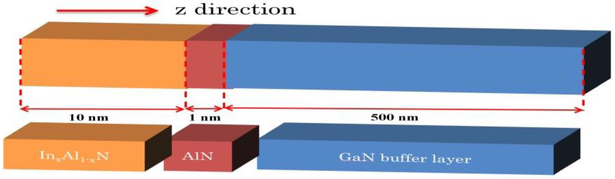
2. Modeling and Theory

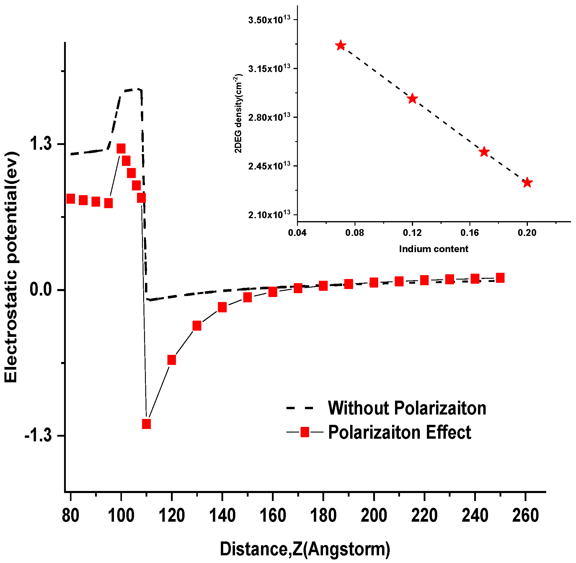
2.1. Polarization Effect

The schematic of InxAl1−xN/AlN/GaN heterostructure studied in this work is given in Figure 1. The heterostructure consists of a 500 nm thick unintentionally doped GaN layer followed by the growth of 10 nm thickness of an In0.12Al0.88N epitaxial layer over it. A thin 1 nm AlN interlayer was inserted to provide sufficient separation of the electron wave from the InAlN. We assumed that the layer of heterostructure would grow on the thick GaN substrate pseudo-morphically along [001], denoted as the z direction in the following figure.
Since the electronic transport properties change considerably due to piezoelectric polarization arising from material strain, the model starts with the calculation for diagonal strain components modeled by
ε x x = ( a 1     a 2 ) / a 2
ε z z =     ε x x ( C 13 / C 33 )
where a 1 , a 2 are the lattice parameters of the different layers, ε x x , ε z z are bi-axial strain and uni-axial strain, which refer to the direction of parallel and perpendicular to the grown interface respectively. As strain and piezoelectric physical constants are known, piezoelectric polarization at each heterointerface can be calculated with [29,30].
P P E = 2 ε z z ( e 31 e 33 C 13 C 33 )
where C 13 , C 33 are elastic constants. The ternary material of InxAl1−xN is calculated with parameters given in Table 1 following Vegard’s law.
P I n A l N sp ( x ) = x P I n N sp + ( 1 x ) P A l N sp + b x ( 1 x )
where b is the bowing parameter (b = 0.07 C/m2) [31], x is the indium content.
For a generic InxAl1−xN/GaN based HEMT structure, the indium content dependent sheet carrier density n s ( x ) is given by [32,33]
n s ( x ) = σ ( x ) q ( ε 0 ε ( x ) d q 2 ) [ q φ b + E f ( x ) Δ E c ( x ) ]
Following the analysis of references [33,34], n s may also be related to the gate and channel voltage through Gauss law as
q n s = C eff ( V g V off φ s ( V ch ) )
φ s ( V ch ) = V ch + E f ( V ch )
In Equations (5) to (7), σ is the combination of the spontaneous polarization and piezoelectric charge which is determined by Equations (3) and (4) respectively, ε is the dielectric constant, d is the InAlN barrier thickness, φ b is the Schottky barrier height, E f is the Fermi energy level with respect to the GaN conduction band, Δ E c represents the conduction band discontinuity given by Δ E C , A B N ( x ) = 0.7 [ E g , A B N ( x ) E g , A B N ( 0 ) ] , the concept of effective band offset (Equation (3) in [21]) is used when the effect of AlN layer is taken into account, C eff is effective capacitance (per unit area) between the gate and 2DEG, V off is cut-off voltage below which it is under sub-threshold region. The surface potential φ s is the Fermi level in the body where the channel voltage V ch = V s at the source and V ch = V d s at the drain respectively.

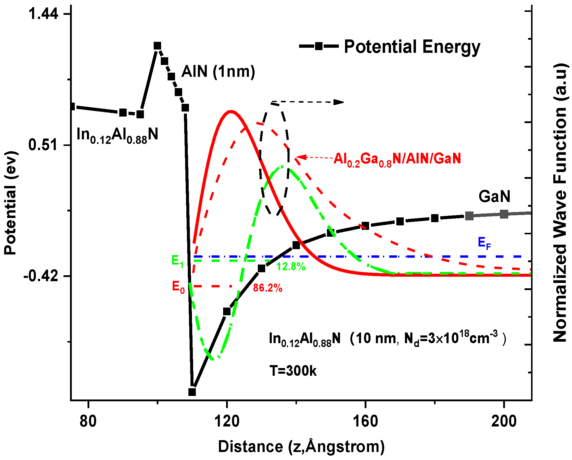
2.2. Self-Consistent Calculations

In the framework of the effective mass approximation, the following calculations of the Eigen-states for electron are taken into account:
[ 2 2 m * d 2 ξ i ( z ) d z 2 ] + [ E c ( z ) E i ] ξ i ( z ) = 0
d d z ( ε o ε ( z ) d E c ( z ) d z ) = q [ n 2 d ( z ) + n 3 d ( z ) ]
where
E c ( z ) = q φ ( z ) + Δ E c
n 2 d ( z ) = i = 0 + m * k T π 2 ln [ 1 + exp ( E f E i k T ) ] | ξ i ( z ) | 2
n 3 d ( z ) = N D + ( z ) N A ( z )
In Equations (8) to (12), k is the Boltzmann constant, is the Planck constant, m* is effective mass, φ ( z ) is electrostatic potential. E i is energy of the ith sub-band level and ξ i ( z ) is the corresponding wave function. ε ( z ) is the position-dependent dielectric constant, N D + , N A are the bulk densities of the ionized donors and acceptor, respectively. Note that the total sheet charge in this work consists of two parts: the first part is derived from the polarization induced charge calculated by the combination of Equations (3) and (4). Another part comes from the terms which are assumed to be insensitive to quantization, i.e., the ionized dopant concentrations N D + and N A as given in Equation (12). These two components are assumed to be independent of each other.
Our calculation is based on the solving the coupled Schrödinger and Poisson’s equation set given in Equations (8) and (9). A finite iteration scheme is deployed similarly to the approach given in references [23,35]. For InAlN/AlN/GaN HEMT, the boundary conditions are given as follows: at the metal-semiconductor interface, the potential above the Fermi level is the Schottky barrier height. This barrier energy of the heterostructure is set as 1.2 eV relative to the ground energy is defined to the energy level close to the substrate.
At the beginning, one starts with an initial empirical potential φ 0 ( z ) then calculates the wave function ξ i ( z ) as well as the corresponding eigenenergies E i using Schrödinger’s equation. Thereafter, n i is calculated by n n i = m * k T π 2 ln [ 1 + exp ( E F E i k T ) ] and the electron distribution is calculated using Equation (11). The new value of n ( z ) along with N D + and N A are used for calculating potential distribution through using of Equations (9) and (10). This updated value of E c ( z ) will be used in Schrödinger’s equation to find the new wave function and eigenenergies. The iteration process is repeated until convergence criterion is finally achieved. However, the abovementioned procedure does not converge all the time due to the high sensitivity of the eigenenergies on the potential and of the quantum charge n 2 d on the corresponding energy levels. An improved iterative scheme is developed to get around this problem. In this frame work, for each i-th subband, at the n-th iterative step, we define a set of space-dependent energies E i n ( z ) and effective state density N i n ( z ) given as
E i n ( z ) = E i n E i n ( z )
N i n ( z ) = m * k T π 2 | ξ i n ( z ) | 2
The corresponding quantum charge is then defined as
n 2 d n + 1 ( z ) = i = 0 + N i n ( z ) log [ 1 + exp ( E f E c n + 1 ( z ) E i n ( z ) k T ) ]
At step n + 1 , Equation (15) will be included into the Poisson’s equation (9), and this equation will be solved for determining the updated E c n + 1 . Note that we involve the term of space dependent E i n ( z ) in Equation (13) so as to overcome the numerical oscillations during the feedback of iterative calculation. This dependence finally vanishes when the algorithm reaches convergence at E c n = E c n + 1 , and Equation (15) gives the same charge density as Equation (11).
On the other hand, in a classical system, one uses the concept of effective density of state N c and the order 1/2 Fermi-Dirac integral when accounting for the local dependence of electron concentration on the potential. In that case, the right term of Equation (9) can be replaced by
n = N c F 1 / 2 ( ( E f E c ( z ) ) / k T )
This approximate model is compared with our quantum effect calculation to reveal how these quantum mechanicals influence the InAlN/GaN-based HEMT performance.

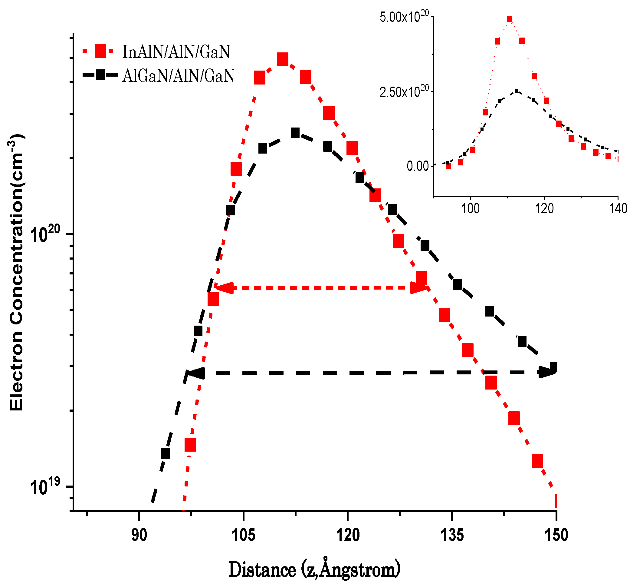
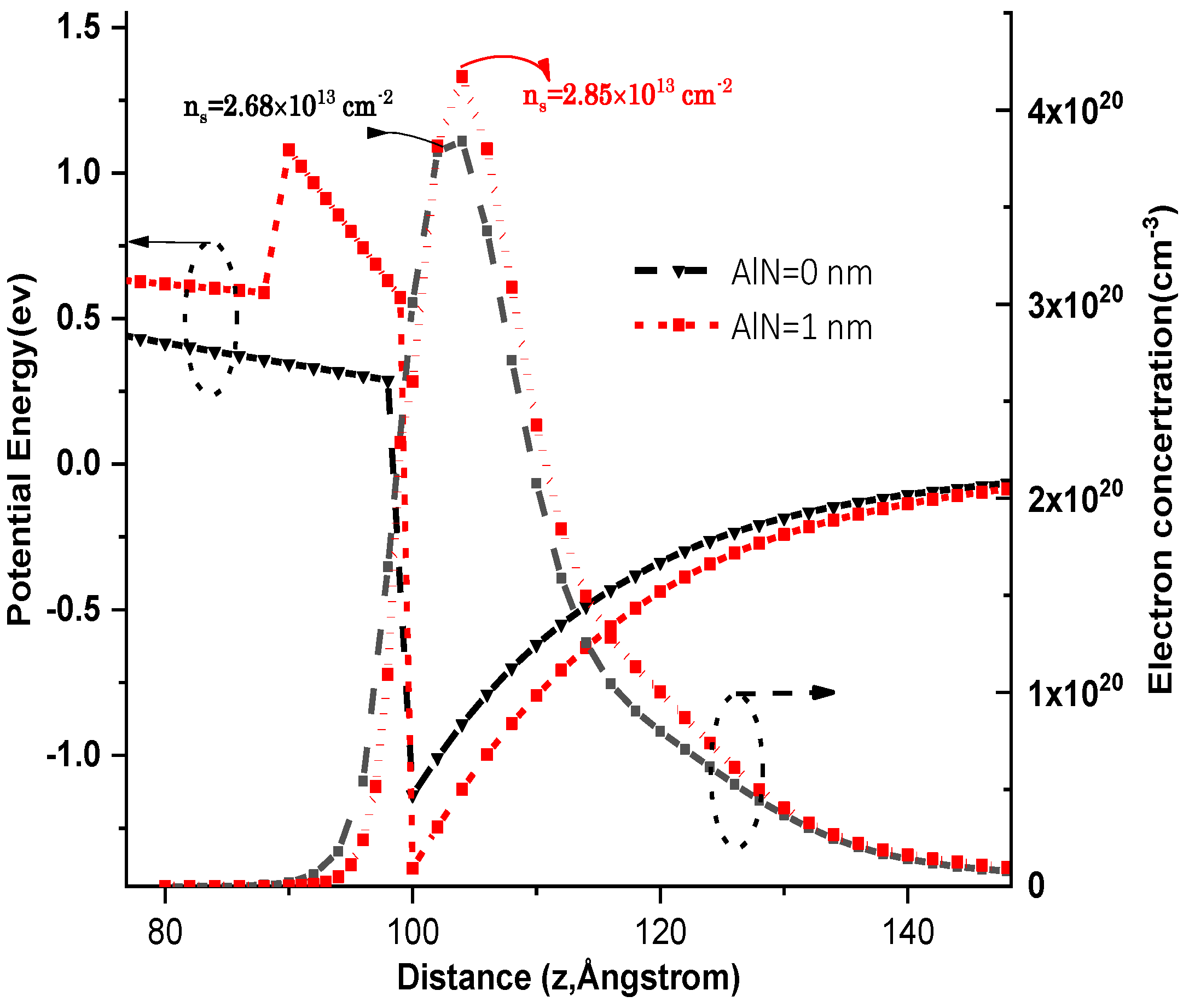
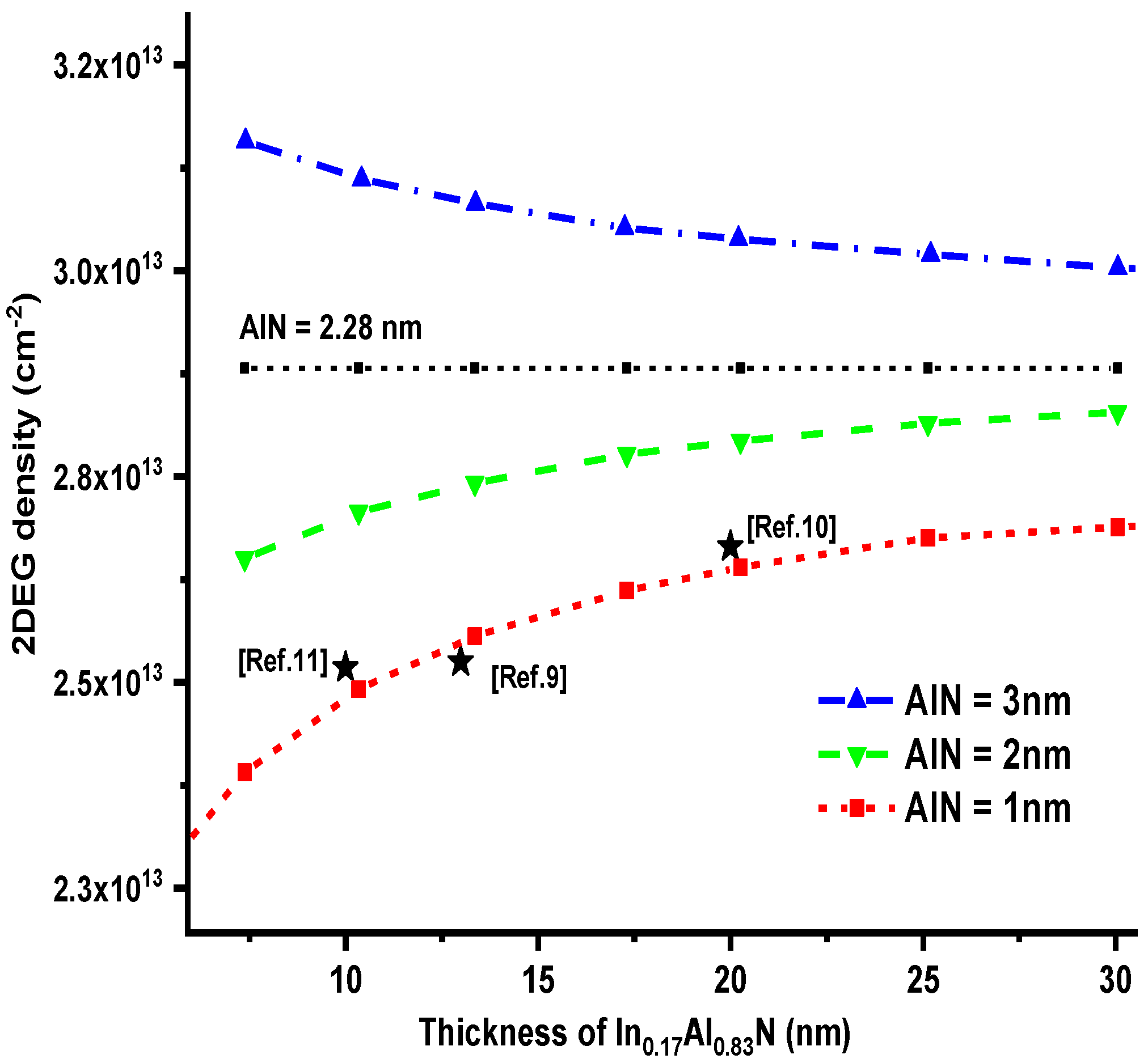
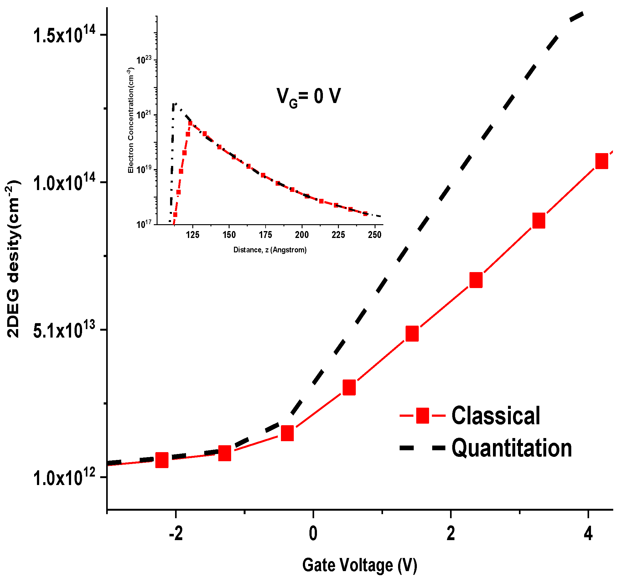
3. Results and Discussion

The calculations were carried out at room temperature for the InxAl1−xN/AlN/GaN structure given in Figure 1. In the following, the barrier indium content is assumed to be ranging from 0.03 to 0.23. The ionized dopant concentrations N d + and residual N A in the buffer layer are assumed to be 3 × 10 18 cm−3 and 1 × 10 13 cm−3 respectively unless otherwise stated. Other physical constants used in this calculation are summarized in Table 1.
Figure 2 shows the sketch of the band bending with (solid, red) and without (dash, black) the polarization effect, along with the calculated 2DEG density from the polarization induced sheet charge given in the inset. To incorporate the contribution of polarization effect, a bound sheet charge width approximately ~6 Å width [30] is added at the AlN/GaN interface in our self-consistent calculation. We use the indium fraction x as a variable parameter to alter the sheet carrier density so that the sheet density of electron satisfies both Equations (5) and (11). As seen from Figure 2, the polarization effect dominates the behavior of electrostatic potential within the vicinity of the heterojunction. The 2D channel becomes sharper and the confined electrons are pushed close to the interface. Note that the 2DEG density increases almost linearly with the decreasing of the In fraction (corresponding to increasing of Al fraction) as indicated in the inset of Figure 2. i.e., for a representative 10 nm InAlN barrier heterostructure, the sheet carrier density is calculated to be 2.55 × 10 13 cm−2 for the In fraction of x   =   0.23 and may be increased to 3.3 × 10 13 cm−2 for x   =   0.07 . When the fraction of indium is around 17–18%, InAlN is assumed to be lattice matched with GaN material, the heterostructure is free of strain (effect of piezoelectric polarization vanishes, P P E = 0 ) and the polarization charge for the interface is mainly determined by the spontaneous effect given by Equation (4).
Figure 3 presents the conduction band profile of the In0.12Al0.88N/AlN/GaN heterostructure with barrier thickness of 10 nm and AlN interlayer thickness of 1 nm, along with the wave functions representing the probability distribution of electrons of the corresponding energy level. For the sake of simplicity, only the ground state and first exited state ( i   =   0 , 1 ) are considered. The numbers given in Figure 3 indicate the probability occupation of the corresponding subband energy. The wave function within the ground state of a similar Al0.2Ga0.8N/AlN/GaN heterostructure is also given for comparison. For a 10 nm In0.12Al0.88N/AlN/GaN heterostructure, over 86.2% of the channel electrons are occupied by the ground state, suggesting the formation of 2DEG system at AlN/GaN interface. The variation of the ground and first exited subband ( E 1 E 0 ) is around 179 meV at the room temperature as compared with 72 meV for that of Al0.2Ga0.88N/GaN. A larger energy separation implies a stronger electrical field and better 2DEG confinement, as shown in the result given in Figure 4.
To quantify the 2DEG confinement characteristics, we approximately define the width of two-dimensional electron gas as the variation between the two depths at which the electron concentration shrunk to 10% of its maximum value. As seen from Figure 4, the 2DEG width is around 5.4 nm for a 10 nm Al0.2GaN0.8N barrier, and this amount deceases to ~3.3 nm as observed in a comparable In0.12Ga0.88N structure. An improved carrier confinement shows fundamental advantages in suppressing the short-channel effect, i.e., DIGBL, self-heating as suggested in references [36,37,38]. The reduction in short-channel effect helps to increase the frequency performance of GaN-based heterostructure devices.
The electron distribution of In0.12Al0.88N/AlN/GaN depending on AlN thickness is shown in Figure 5. A simple In0.12Al0.88N/GaN structure (AlN = 0 nm) is also given for comparison. For the InAlN/AlN/GaN with a 1 nm AlN interlayer insertion, the electron concentration at the interface increases slightly due to the enlarged band offset over the barrier. There is only an order of 5.3% of the electron density penetrated into the barrier with the penetration width of around 8.2 Å. For AlN interlayer thickness larger than 1 nm, little influence was observed on the wave function and charge distribution.
The 2DEG density in dependence on the barrier thickness for a lattice-matched In0.17Al0.83N/AlN/GaN heterostructure is given in Figure 6. The AlN thickness varies from 1 to 3 nm. The result of Figure 6 comes from the calculated maximum sheet density located at the interface of the AlN/GaN structure. Other parameters are kept the same as in Figure 5. The calculated results have been compared with the available experimental data given in references [9,10,11]. A reasonable agreement is achieved justifying the validation of this work. It was found that the 2DEG sheet density increases as AlN thickness increases. The insertion of the AlN layer tends to weaken the increasing dependence of 2DEG density on the barrier thickness. For 1 nm AlN layer, the sheet density of 2DEG increases with the barrier thickness and then tends to saturate. This trend is profoundly contrary to the case when increasing AlN thickness to 3 nm. According to the theoretical calculation, a critical AlN thickness (~2.28 nm for lattice-matched In0.17Al0.83N/AlN/GaN) may exist at which little variation occurs on the 2DEG density when increasing InAlN thickness, as shown in Figure 6. It is now clear that the InAlN barrier predominately induces the 2DEG for a thinner AlN layer, however, the AlN layer takes the dominant contribution to 2DEG formation when it is thick enough. A similar phenomenon was also observed in an AlN/GaN structure [22].
To clarify the impact of quantization effect on realistic devices, a generic InxAl1−xN/AlN/GaN-based HEMT is utilized to study the channel concentration dependence on the applied gate voltage by using different models. The result is shown in Figure 7 wherein the electron distribution at V G = 0 V is given in the inset. The boundary conditions are given as following: the conduction band edge at gate on the InAlN is fixed to the Schottky-barrier height (1.2 eV) and the applied voltage. The channel is under grounded ( V ch = 0 ) and Fermi level is fixed to a sufficiently small value below 1 × 10 4 × ( k T / q ) . Only the ground state and first exited state ( i = 0 , 1 ) are taken into account. The corresponding wave functions are assumed to be vanished at boundaries of the structure. Other calculation parameters are kept the same as with Figure 3.
As for the quantum mechanical results, the maximum of the electron concentration is found to be located at around several angstroms from the interface instead of the interface as predicted by the classical model. This result coincides with the charge width approximation given in Figure 2 previously. The cut off voltage V off is found to be mainly determined by the polarization charge present at the heterointerface. It is worth noting that when channel carrier density does not exceed ~ 6 × 10 12 cm−2, even the classical model simply through the density of state N c using Equation (16) can evaluate the channel electron within a 5 percent error. The deviation starts to gradually enhance when sheet carrier density reach to 2.3 × 10 13 cm−2 (corresponding to electric field order of ~3.8 MV/cm at interface). The result implies that the behavior of InAlN/GaN–based HEMT under the sub-threshold region may be described with good accuracy even by the classical approach using Fermi-Dirac statistics. As for increasing the applied gate voltage, the conduction band can no longer be treated as a continuous state due to the enlarged electric field. In this condition, a significant quantization effect may arise when dealing with transport properties of the 2DEG in these small-geometry devices.

4. Conclusions

A comprehensive model of 2DEG characteristic of InxAl1−xN/AlN/GaN heterostructure has been given in this paper taking polarization and quantum mechanical effect into account. We report a detailed study on the 2DEG density and electron distribution across the heterostructure using a solution of Schrödinger and Poisson’s equations solved through an improved iterative scheme.
It is found that that the polarization effect dominates the behavior of electrostatic potential within the vicinity of the heterojunction. Due to the strong polarization field, a thinner electron distribution profile of In0.12Al0.88N/AlN/GaN is observed as being comparable with the AlGaN/AlN/GaN structure. Therefore, improving the quality of interface roughness is essential for enhancing the transport property in these structures. A critical AlN thickness (~2.28 nm) was predicated when considering the 2DEG density in dependence on a lattice matched In0.17Al0.83N thickness. It is clear that the InAlN barrier predominately induces the 2DEG for a thinner AlN layer (1 nm), however, the AlN layer dominates the contribution to 2DEG formation when it grows beyond critical thickness.
We found the carrier transport for a generic InAlN/GaN-based HEMT under sub-threshold region can be well described even by the classical approach using Fermi-Dirac statistics. As the gate voltage increases, both the polarization charge and applied voltage give rise to potential well and the conduction band has been splitted into discrete sub-bands. A significant quantization effect also arises and must be carefully treated to achieve a reliable description of those small-geometry devices.
Although some previous C-V measurements indicate that many-body effects such as exchange and correlation energies are of importance [24,26,27], these effects have been neglected for the sake of simplicity. Nevertheless, since these effects can actually affect device performance, more work should be dedicated to these effects in future so as to find an easy way to incorporate them into Schrödinger’s equation. The application of the presented results given in this work server as a guide for optimization of the epilayer structure in engineering, and would always be a substantial improvement with respect to the widely adopted semi-classical model.

Author Contributions

Conceptualization, J.Q.; Investigation & Methodology, J.Q.; Validation, J.Q. and B.y.L.; Formal analysis, J.Q. and Q.b.Z.; Writing—original draft preparation, J.Q. and Q.b.Z.; Writing—review and editing, H.W.; Supervision, H.W.

Funding

This research was funded by Science and Technologies plan Projects of Guangdong Province (Nos. 2017B010112003, 2017A050506013), and by Applied Technologies Research and Development Projects of Guangdong Province (Nos. 2015B010127013, 2016B010123004), and by Science and Technologies plan Projects of Guangzhou City (Nos. 201504291502518, 201605030014, 201604046021, 201704030139), and by Science and Technology project of Guangzhou Education Municipality (No. 201630328), and by Science and Technology Development Special Fund Projects of Zhongshan City (Nos. 2017F2FC0002, 2017A1009).

Conflicts of Interest

The authors declare no conflict of interest. The funders had no role in the design of the study.

References

  1. Shen, L.; Heikman, S.; Moran, B.; Coffie, R. AlGaN/AlN/GaN high-power microwave HEMT. IEEE Electron. Device Lett. 2001, 22, 457–459. [Google Scholar] [CrossRef]
  2. Palacios, T.; Chakraborty, A.; Heikman, S.; Keller, S.; DenBaars, S.P.; Mishra, U.K. AlGaN/GaN high electron mobility transistors with InGaN back-barriers. IEEE Electron. Device Lett. 2006, 27, 13–15. [Google Scholar] [CrossRef]
  3. Menozzi, R.; Umana-Membreno, G.A.; Nener, B.D.; Parish, G.; Sozzi, G.; Faraone, L.; Mishra, U.K. Temperature-Dependent Characterization of AlGaN/GaN HEMTs: Thermal and Source/Drain Resistances. IEEE Trans. Device Mater. Reliab. 2008, 8, 255–264. [Google Scholar] [CrossRef]
  4. Hao, Y.; Yang, L.; Ma, X.; Ma, J.; Cao, M.; Pan, C.; Wang, C.; Zhang, J. High-Performance Microwave Gate-Recessed AlGaN/AlN/GaN MOS-HEMT With 73% Power-Added Efficiency. IEEE Electron. Device Lett. 2011, 32, 626–628. [Google Scholar] [CrossRef]
  5. Shinohara, K.; Regan, D.C.; Tang, Y.; Corrion, A.L.; Brown, D.F.; Wong, J.C.; Robinson, J.F.; Fung, H.H.; Schmitz, A.; Oh, T.C.; et al. Scaling of GaN HEMTs and Schottky Diodes for Submillimeter-Wave MMIC Applications. IEEE Trans. Electron. Devices 2013, 60, 2982–2996. [Google Scholar] [CrossRef]
  6. Yu, T.H.; Brennan, K.F. Theoretical study of the two-dimensional electron mobility in strained III-nitride heterostructures. J. Appl. Phys. 2001, 89, 3827–3834. [Google Scholar] [CrossRef]
  7. Yarar, Z.; Ozdemir, B.; Ozdemir, M. Electron mobility in a modulation doped AlGaN/GaN quantum well. Eur. Phys. J. B 2006, 49, 407–414. [Google Scholar] [CrossRef]
  8. Meng, F.; Zhang, J.; Zhou, H.; Ma, J.; Xue, J.; Dang, L.; Zhang, L.; Lu, M.; Ai, S.; Li, X.; et al. Transport characteristics of AlGaN/GaN/AlGaN double heterostructures with high electron mobility. J. Appl. Phys. 2012, 112. [Google Scholar] [CrossRef]
  9. Gonschorek, M.; Carlin, J.-F.; Feltin, E.; Py, M.A.; Grandjean, N. High electron mobility lattice-matched AlInN/GaN field-effect transistor heterostructures. Appl. Phys. Lett. 2006, 89, 062106. [Google Scholar] [CrossRef]
  10. Jeganathan, K.; Shimizu, M.; Okumura, H.; Yano, Y.; Akutsu, N. Lattice-matched InAlN/GaN two-dimensional electron gas with high mobility and sheet carrier density by plasma-assisted molecular beam epitaxy. J. Cryst. Growth 2007, 304, 342–345. [Google Scholar] [CrossRef]
  11. Pietzka, C.; Denisenko, A.; Alomari, M.; Medjdoub, F.; Carlin, J.-F.; Feltin, E.; Grandjean, N.; Kohn, E. Effect of Anodic Oxidation on the Characteristics of Lattice-Matched AlInN/GaN Heterostructures. J. Electron. Mater. 2008, 37, 616–623. [Google Scholar] [CrossRef]
  12. Dasgupta, S.; Lu, J.; Speck, J.S.; Mishra, U.K. Self-Aligned N-Polar GaN/InAlN MIS-HEMTs With Record Extrinsic Transconductance of 1105 mS/mm. IEEE Electron. Device Lett. 2012, 33, 794–796. [Google Scholar] [CrossRef]
  13. Smith, M.D.; O’Mahony, D.; Conroy, M.; Schmidt, M.; Parbrook, P.J. InAlN high electron mobility transistor Ti/Al/Ni/Au Ohmic contact optimisation assisted by in-situ high temperature transmission electron microscopy. Appl. Phys. Lett. 2015, 107, 4. [Google Scholar] [CrossRef]
  14. Tsou, C.W.; Lin, C.Y.; Lian, Y.W.; Hsu, S.S.H. 101-GHz InAlN/GaN HEMTs on Silicon with High Johnson’s Figure-of-Merit. IEEE Trans. Electron. Devices 2015, 62, 2675–2678. [Google Scholar] [CrossRef]
  15. Miao, Z.L.; Tang, N.; Xu, F.J.; Cen, L.B.; Han, K.; Song, J.; Huang, C.C.; Yu, T.J.; Yang, Z.J.; Wang, X.Q.; et al. Magnetotransport properties of lattice-matched In0.18Al0.82N/AlN/GaN heterostructures. J. Appl. Phys. 2011, 109, 016102. [Google Scholar] [CrossRef]
  16. Xue, J.; Zhang, J.; Hao, Y. Demonstration of InAlN/AlGaN high electron mobility transistors with an enhanced breakdown voltage by pulsed metal organic chemical vapor deposition. Appl. Phys. Lett. 2016, 108, 013508. [Google Scholar] [CrossRef]
  17. Zhou, H.; Lou, X.; Conrad, N.J.; Si, M.; Wu, H.; Alghamdi, S.; Guo, S.; Gordon, R.G.; Ye, P.D. High-Performance InAlN/GaN MOSHEMTs Enabled by Atomic Layer Epitaxy MgCaO as Gate Dielectric. IEEE Electron. Device Lett. 2016, 37, 556–559. [Google Scholar] [CrossRef]
  18. Chen, P.G.; Tang, M.; Liao, M.H.; Lee, M.H. In0.18Al0.82N/AlN/GaN MIS-HEMT on Si with Schottky-drain contact. Solid-State Electron. 2017, 129, 206–209. [Google Scholar] [CrossRef]
  19. Xing, W.; Liu, Z.; Qiu, H.; Ranjan, K.; Gao, Y.; Ng, G.I.; Palacios, T. InAlN/GaN HEMTs on Si With High fT of 250 GHz. IEEE Electron. Device Lett. 2018, 39, 75–78. [Google Scholar] [CrossRef]
  20. Medjdoub, F.; Carlin, J.; Gonschorek, M.; Feltin, E.; Py, M.A.; Ducatteau, D.; Gaquiere, C.; Grandjean, N.; Kohn, E. Can InAlN/GaN be an alternative to high power/high temperature AlGaN/GaN devices? In Proceedings of the 2006 International Electron Devices Meeting, San Francisco, CA, USA, 11–13 December 2006; pp. 1–4. [Google Scholar]
  21. Gonschorek, M.; Carlin, J.-F.; Feltin, E.; Py, M.A.; Grandjean, N.; Darakchieva, V.; Monemar, B.; Lorenz, M.; Ramm, G. Two-dimensional electron gas density in Al1−xInxN/AlN/GaN heterostructures (0.03 ≤ x ≤ 0.23). J. Appl. Phys. 2008, 103, 093714. [Google Scholar] [CrossRef]
  22. Kong, Y.C.; Zheng, Y.D.; Zhou, C.H.; Gu, S.L.; Zhang, R.; Han, P.; Shi, Y.; Jiang, R.L. Two-dimensional electron gas densities in AlGaN/AlN/GaN heterostructures. Appl. Phys. A 2006, 84, 95–98. [Google Scholar] [CrossRef]
  23. Lenka, T.R.; Panda, A.K. Characteristics study of 2DEG transport properties of AlGaN/GaN and AlGaAs/GaAs-based HEMT. Semiconductors 2011, 45, 650–656. [Google Scholar] [CrossRef]
  24. Dianat, P.; Persano, A.; Quaranta, F.; Cola, A.; Nabet, B. Anomalous Capacitance Enhancement Triggered by Light. IEEE J. Sel. Top. Quantum Electron. 2015, 21, 1–5. [Google Scholar] [CrossRef]
  25. Skinner, B.; Shklovskii, B. Anomalously large capacitance of a plane capacitor with a two-dimensional electron gas. Phys. Rev. B 2010, 82, 155111. [Google Scholar] [CrossRef]
  26. Li, L.; Richter, C.; Paetel, S.; Kopp, T.; Mannhart, J.; Ashoori, R.C. Very Large Capacitance Enhancement in a Two-Dimensional Electron System. Science 2011, 332, 825–828. [Google Scholar] [CrossRef] [PubMed] [Green Version]
  27. Dianat, P.; Prusak, R.; Persano, A.; Cola, A.; Quaranta, F.; Nabet, B. An Unconventional Hybrid Variable Capacitor with a 2-D Electron Gas. IEEE Trans. Electron. Devices 2014, 61, 445–451. [Google Scholar] [CrossRef]
  28. Ando, T.; Fowler, A.B.; Stern, F. Electronic properties of two-dimmensional systems. Rev. Mod. Phys. 1982, 54, 437–672. [Google Scholar] [CrossRef]
  29. Ambacher, O.; Smart, J.; Shealy, J.R.; Weimann, N.G.; Chu, K.; Murphy, M.; Schaff, W.J.; Eastman, L.F. Two-dimensional electron gases induced by spontaneous and piezoelectric polarization charges in N- and Ga-face AlGaN/GaN heterostructures. J. Appl. Phys. 1999, 85, 3222–3233. [Google Scholar] [CrossRef]
  30. Ambacher, O.; Foutz, B.; Smart, J.; Shealy, J.R.; Weimann, N.G.; Chu, K.; Murphy, M.; Sierakowski, A.J.; Schaff, W.J.; Eastman, L.F.; et al. Two dimensional electron gases induced by spontaneous and piezoelectric polarization in undoped and doped AlGaN/GaN heterostructures. J. Appl. Phys. 2000, 87, 334–344. [Google Scholar] [CrossRef]
  31. Vurgaftman, I.; Meyer, J.R. Band parameters for nitrogen-containing semiconductors. J. Appl. Phys. 2003, 94, 3675–3696. [Google Scholar] [CrossRef]
  32. Yu, E.T.; Sullivan, G.J.; Asbeck, P.M.; Wang, C.D.; Qiao, D.; Lau, S.S. Measurement of piezoelectrically induced charge in GaN/AlGaN heterostructure field-effect transistors. Appl. Phys. Lett. 1997, 71, 2794–2796. [Google Scholar] [CrossRef]
  33. Zhang, J.; Syamal, B.; Zhou, X.; Arulkumaran, S.; Ng, G.I. A Compact Model for Generic MIS-HEMTs Based on the Unified 2DEG Density Expression. IEEE Trans. Electron. Devices 2014, 61, 314–323. [Google Scholar] [CrossRef]
  34. Delagebeaudeuf, D.; Linh, N.T. Metal-(n) AlGaAs-GaAs two-dimensional electron gas FET. IEEE Trans. Electron. Devices 1982, 29, 955–960. [Google Scholar] [CrossRef]
  35. Tan, I.H.; Snider, G.L.; Chang, L.D.; Hu, E.L. A self-consistent solution of Schrödinger–Poisson equations using a nonuniform mesh. J. Appl. Phys. 1990, 68, 4071–4076. [Google Scholar] [CrossRef]
  36. Sadi, T.; Kelsall, R.W.; Pilgrim, N.J. Investigation of self-heating effects in submicrometer GaN/AlGaN HEMTs using an electrothermal Monte Carlo method. IEEE Trans. Electron. Devices 2006, 53, 2892–2900. [Google Scholar] [CrossRef]
  37. Medjdoub, F.; Alomari, M.; Carlin, J.F.; Gonschorek, M.; Feltin, E.; Py, M.A.; Grandjean, N.; Kohn, E. Barrier-layer scaling of InAlN/GaN HEMTs. IEEE Electron. Device Lett. 2008, 29, 422–425. [Google Scholar] [CrossRef]
  38. Chen, C.Y.; Wu, Y.R. Studying the short channel effect in the scaling of the AlGaN/GaN nanowire transistors. J. Appl. Phys. 2013, 113. [Google Scholar] [CrossRef]
Figure 1. Schematic of the InxAl1−xN/AlN/GaN heterostructure studied in this work.
Electronics 07 00410 g001
Figure 2. Sketch of the band bending with (solid, red) and without (dash, black) the polarization effect being taken into account. The calculated 2DEG density for a 10 nm InAlN/AlN/GaN heterostructure as a function of indium fraction is given in the inset.
Electronics 07 00410 g002
Figure 3. The conduction band profile of the In0.12Al0.88N/AlN/GaN heterostructure and the wave function of the ground state (i = 0, red, line) and first excited (i = 1, green, dash) under room temperature. A normalized first subband wave function for an Al0.2Ga0.8N/AlN/GaN (red, short dash) is given for comparison.
Electronics 07 00410 g003
Figure 4. Comparison of the electron distribution of In0.12Al0.88N/AlN/GaN and case of Al0.2Ga0.8N/AlN/GaN for characteristics of 2DEG confinement.
Electronics 07 00410 g004
Figure 5. The electron concentration and conduction band distribution of In0.12Al0.88N/AlN/GaN with different AlN thicknesses.
Electronics 07 00410 g005
Figure 6. The 2DEG sheet density of In0.17Al0.83N/AlN/GaN versus InAlN barrier thickness with different AlN thicknesses, The obtained experimental data from [9,10,11] are given for comparison.
Electronics 07 00410 g006
Figure 7. The gate voltage dependence of the 2DEG density for a generic InAlN/AlN/GaN using classical model (Equation (16)) and quantum mechanical (Equation (11)). The inset presents the electron distribution within the heterostructure at V g = 0 V . The extracted parameters used in calculation are given as: V off = 3.3 V , C eff = 8.36 × 10 6 F / cm 2 , N c = 2.3 × 10 18 cm 3 .
Electronics 07 00410 g007
Table 1. Physics parameters of InN, AlN, and GaN at room temperature [30,31].
Title 1InNAlNGaN
a x (Å)3.5453.1123.189
P sp (C/m2)−0.032−0.081−0.032
e31− (C31/C33)e33 (C/m2)−0.86−0.91−0.69
m e * ( m 0 ) 0.110.480.22
ε x ( ε 0 ) 138.510

