Abstract
This paper presents an optimized single-phase three-level boost DC-link cascade H-bridge multilevel inverter (TLBDCLCHB MLI) system to generate a seven-level stepped output voltage waveform for photovoltaic (PV) applications. The proposed TLBDCLCHB MLI system is obtained by integrating a three-level boost converter (TLBC) with a seven-level DC-link cascade H-bridge (DCLCHB) inverter. It consists of a TLBC, level generation unit (LGU) and phase sequence generation unit (PSGU). When compared with traditional boost converter-fed multilevel inverter systems, the proposed TLBDCLCHB MLI system requires a single DC source, fewer power switches and gate drivers. Reduction in the switch count and number of DC sources makes the system cost effective and requires a smaller installation area. Pulse generation for the power switches of an LGU in a DCLCHB inverter is accomplished by providing proper conducting angles that are generated by optimized conducting angle determination (CAD) techniques. In this paper two CAD techniques i.e., equal-phase CAD (EPCAD) and step pulse wave CAD (SPWCAD) techniques are proposed to evaluate the performance of the proposed system in terms of the total harmonic distortion (THD) and the quality of the stepped output voltage waveform. The proposed system has been modeled and simulated using MATLAB/SIMULINK software. Results are presented and discussed. Also, a prototype model of a single-phase TLBDCLCHB MLI system is developed using a field-programmable gate array (FPGA)-based pulse generation with a resistive load and its performance is analyzed for various operating conditions.
1. Introduction
Development in power electronics lay down a widespread scope for the resourceful operation of power converters. A few setups of power converters are produced to do the sun-powered photovoltaic (PV) applications with enhanced adequacy [1,2]. PV power generation is an encouraging elective source of energy and has numerous focal points compared to the other elective energy sources like wind, ocean, biomass, fuel, geothermal, and so on. In PV power generation, boost converters and multilevel inverters (MLIs) are playing a major role in power conversion. These power converters are broadly being utilized as a connection between load and supply. As most of the renewable power source generation is DC in nature, the DC-DC boost converters are utilized to increase the voltage level, and the DC must be changed over to AC for grid connection. Therefore, MLIs are used for DC to AC conversion [3,4]. The power generation using a traditional boost converter and inverter consists of a greater number of components, requires a larger installation area, is bulky in size, and costly. Also, the traditional boost converters are unable to produce a high boost ratio [5,6]. This paper proposes a three-level boost converter (TLBC) with a high boost ratio, based on one switch, one inductor, (2N-1) capacitors, and (2N-1) diodes for ‘N’ levels. It is a pulse width modulation (PWM)-controlled boost converter capable of maintaining an equal voltage in all ‘N’ output levels and controlling the input current.
In this paper, the structure of single-phase three-level boost DC-link cascade H-bridge multilevel inverter (TLBDCLCHB MLI) system is proposed to generate a seven-level stepped output voltage waveform for PV applications. The proposed system is obtained by integrating a three-level boost converter (TLBC) with a seven-level DC-link cascade H-bridge (DCLCHB) [7,8]. Also, the objective of the proposed work is to investigate the performance of a single-phase seven-level DCLCHB inverter [9,10] using conducting angle determination (CAD) techniques [11] in terms of the total harmonic distortion (THD) and the quality of the stepped output voltage waveform. Here, equal-phase CAD (EPCAD) based on equal-area distribution and step pulse wave CAD (SPWCAD) based on volt-second area equal to step pulse wave techniques are proposed to evaluate the performance of the DCLCHB inverter [12]. The proposed TLBDCLCHB MLI system is modeled, simulated and validated through experimental setup using field-programmable gate array (FPGA)-based pulse generation.
2. Structure of TLBDCLCHB MLI System
The block diagram of the proposed TLBDCLCHB MLI system is shown in Figure 1. The proposed TLBDCLCHB MLI system consists of single DC voltage source, TLBC, and DCLCHB inverter to generate a seven-level stepped output waveform. The DCLCHB inverter is composed of level generation unit (LGU) and phase sequence generation unit (PSGU). LGU is used to generate the required number of levels and PSGU is used to generate positive and negative sequence voltage levels [13]. The equivalent structure of TLBDCLCHB MLI system is shown in Figure 2.
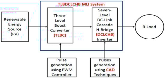
Figure 1.
Block diagram of the proposed (TLBDCLCHB MLI) system.
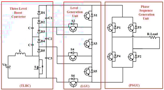
Figure 2.
Equivalent structure of TLBDCLCHB MLI system.
The number of power switches ‘NSwitches’ and the number of levels ‘m’ for a single-phase TLBDCLCHB MLI system are calculated using Equations (1) and (2), respectively.
where ‘C’ is the number of DC link capacitors integrated to a DCLCHB inverter and ‘H’ is the number of H-Bridge circuits.
Table 1 demonstrates the required number of power switches and DC sources for the traditional and proposed boost DC-link-based inverter to generate a stepped output waveform from seven levels to fifteen levels. From the investigation, it is gathered that the proposed TLBDCLCHB MLI system has reduced the switch count and requires just a single DC source compared to traditional boost multilevel inverter (MLI) systems [14,15].

Table 1.
Component requirements for existing and proposed boost based MLI systems.
3. Three-Level Boost Converter (TLBC)
The circuit configuration of DC-DC TLBC is represented in Figure 2. It consists of a traditional boost converter, (2N-1) capacitors, and (2N-1) diodes. The main advantages of using the TLBC topology are; it can be extended to any number of levels by adding only diodes and capacitors without changing the main circuit; no need of additional voltage balance circuit; and voltage gain can be increased without the use of a transformer by operating at minimum duty ratio. The TLBC circuit consists of three stages which are operated by varying duty cycles of 0.4, 0.5, and 0.6. The operation of the TLBC is explained in [16].
3.1. Analysis of DC-DC TLBC
Considering the presence and absence of inductor power loss for both traditional and proposed TLBCs gives important information to designers. From basic principles, the voltage gain or the boost factor of the traditional boost converter [14] is given by Equation (3):
where ‘Vo’ is the output voltage, ‘Vdc’ is the input voltage and ‘D’ is the duty cycle.
By considering the lossless system, the voltage gain for the N-level boost converter can be expressed as:
For a lossless system, the input current, Idc, can be expressed as:
From Equation (5), the input current, Idc, can be controlled using duty cycle ‘D’ in the PWM. Now the voltage gain or boost factor expression for the N-level boost converter can be derived as follows:
Based on the condition that the average voltage across the inductor ‘L’ is equal to zero. The total inductor voltage during the ON—OFF condition can be expressed as,
where, ‘IL’ is the inductor current which is equivalent to ‘Idc’ and ‘RL’ is the inductor resistance or parasitic resistance.
Here, the first term of Equation (6) is valid when the switch ‘S’ is turned ON, and the second term can write when the switch ‘S’ is turned OFF. From Equation (6) it can be written as,
From Equation (7),
Therefore, from Equations (3)–(7), the input voltage, Vdc can be expressed as,
Therefore, Equation (9) can be expressed as follows:
Equation (10) is equal to Equation (3) if N = 1 and RL = 0. From Equation (10), it can be observed that the voltage gain reaches a maximum before D = 1, and then becomes 0. The effect of parasitic resistance ‘RL’ is responsible for the limitation in the boost factor. The actual boost factor or voltage gain against the duty cycle is analyzed by varying ‘RL’ in Equation (10). Figure 3 and Figure 4 describe the graph between voltage gain versus duty cycle for the traditional boost converter, i.e., N = 1 and for the proposed TLBC, i.e., N = 3 using different values of RL/Ro.
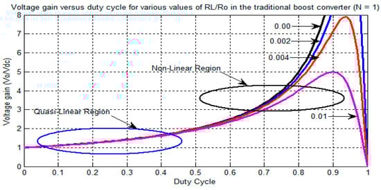
Figure 3.
Duty cycle versus voltage gain of a traditional boost converter for various values of RL/Ro (N = 1).
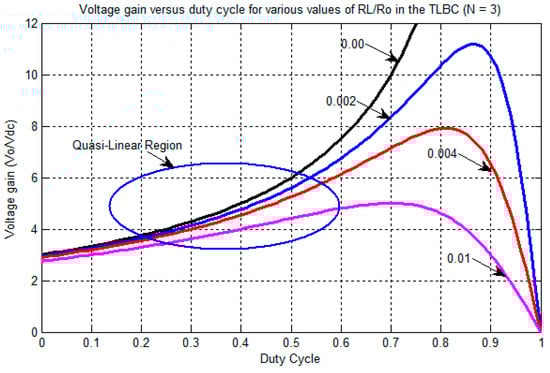
Figure 4.
Duty cycle versus voltage gain of TLBC for various values of RL/Ro (N = 3).
From the Figure 3 and Figure 4, it can be noticed that the voltage gain of the traditional boost converter is quasi-linear when the duty cycle varies from 0 to 0.5, but beyond that, the boost factor of a traditional boost converter becomes non-linear; therefore, the control of a traditional boost converter is complicated.
Similarly, from Figure 4, i.e., when N = 3, it can be observed that the quasi-linear region is extended with a high voltage gain for the TLBC. Therefore, the TLBC achieves a high voltage gain compared to the traditional boost converter, and, also a better operating point of the duty cycle for the TLBC, which is from 0.4 to 0.6.
In the next section, the effect of the voltage drop across the switch and diodes is studied.
3.2. TLBC Voltage Drop Across Switch and Diodes
In actual operation of TLBC, the voltage drop across the switch and diodes must be considered since it avoids full charge across the capacitors [17,18]. Therefore, it reduces the conversion efficiency of the TLBC topology. In general, the voltage drop in the power switches and diodes can be around 2 V, and it can be neglected in medium- and high-voltage applications but must be considered in low-voltage applications. Here, the voltage drop across the switch and diodes is assumed to be equal to ‘Vd’.
From Figure 5, it can be noticed that the voltage across the C5 becomes,
where, ‘2Vd’ is the voltage drop across the switch ‘S’ and diode ‘D5′.
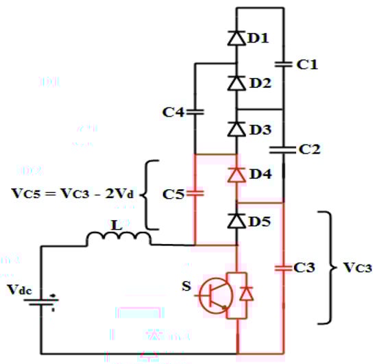
Figure 5.
Charging C5 of a TLBC with switch and diode’s voltage drop.
Similarly, VC2 and VC1 can be written as,
where, VC2 and VC1 are the expressions for the voltage output of two-level and three-level boost converters, respectively. The generalized output voltage expression for the N-level boost converter can be expressed as follows:
where, ‘VC’ is the lower capacitor output voltage, and follows Equation (3).
Equation (14) gives the output voltage for the multiple stages of the boost converter. The efficiency of the proposed converter for the N-level is given by the Equation (15).
Form Equation (15), the efficiency of the TLBC circuit can be reduced by considering the voltage drop across the switch and diode.
3.3. Closed-Loop Control of TLBC
From Figure 5 and Equation (10), it can be observed that the output voltage gain depends on the ratio of load resistance (RO) and source resistance (RL), i.e., if there is any variation between the load and source resistances, the output voltage of TLBC is not kept constant, and, from Equation (13), there will be a variation in the duty cycle to get the required amount of output voltage by considering the voltage drop across the switch and diodes. Therefore, the proposed TLBC circuit is modeled in closed-loop mode using an integral controller to maintain the constant output voltage.
Figure 6 represents the TLBC circuit in closed-loop mode. In the case of any variation in the load side or source side, the output changes, so a suitable controller is designed to change the duty cycle by comparing ‘Vref’ with ‘Vout’ in order to maintain the required output voltage.
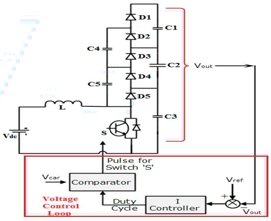
Figure 6.
Model of TLBC in closed-loop mode.
4. DC-Link Cascade H-Bridge (DCLCHB) Inverter
Figure 7 depicts the DCLCHB inverter topology for the generation of a single-phase seven-level output voltage waveform. It is composed of LGU and PSGU [12].
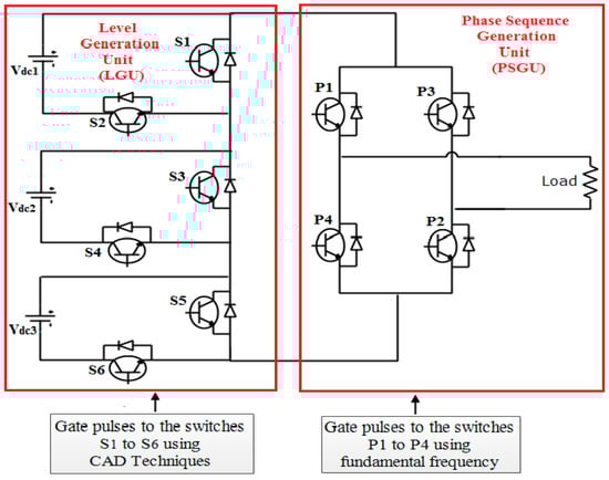
Figure 7.
Single-phase seven-level DCLCHB inverter.
Switches in the LGU are used to generate the required number of levels and it is formed by connecting half-bridge cells in series. Each half-bridge cell consists of a DC source controlled by two switches. PSGU consists of an H-bridge circuit, which is used to generate the positive and negative sequence voltage levels. Table 2 gives a component requirement to generate a seven-level output voltage for the proposed and existing MLIs. It clearly shows a substantial component reduction when using a DCLCHB structure [7,8].
Table 2.
Component requirements for existing and proposed cascade MLI systems.
In this DCLCHB inverter topology, all the magnitudes of DC voltage sources are equal (Vdc1 = Vdc2 = Vdc3).
i.e., Vdci = Vdc, where i = 1, 2, and 3
The maximum value of the output phase voltage is obtained by using Equation (17).
The number of output phase voltage levels can be obtained from Equation (1). The number of power switches for the DCLCHB inverter can be calculated using Equation (18).
Equation (16) gives the output level of the LGU. By using PSGU, the positive and negative levels are obtained at the load (Vo), the synthesized stepped AC output phase voltage will be obtained by using the Equations (19) and (20).
For a single-phase seven-level DCLCHB inverter, the switching sequences to generate the required levels are given in Table 3.
Table 3.
Switching sequence to generate seven-level output for a DCLCHB inverter.
5. Conducting Angle Determination (CAD) Techniques
CAD techniques are a vital part of any inverter since they are directly related to the efficiency of the entire system [6,12]. It is used to control the proposed DCLCHB inverter output phase voltage and also for the calculation of the two main parameters such as %THD and Vrms. In this paper, a step pulse wave CAD (SPWCAD) technique has been employed to trigger the switches of LGU in the DCLCHB inverter and is compared with a conventional CAD technique, i.e., equal-phase CAD (EPCAD) technique. The generation of the seven-level stepped voltage waveform using CAD techniques is shown in Figure 8.
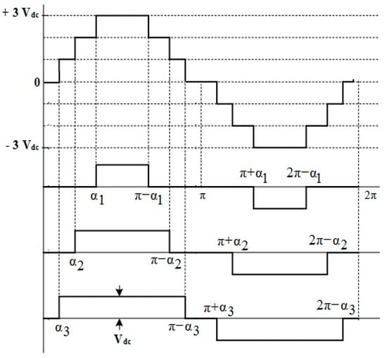
Figure 8.
Generation of the seven-level stepped voltage waveform for DCLCHB inverter using CAD techniques.
In the presented EPCAD and SPWCAD techniques, for an m-level stepped waveform in the period of the first quadrant, i.e., 0 to 90°, 2(m − 1)/2 conducting angles need to be determined. From Figure 8, to generate a seven-level stepped waveform in the first quadrant, i.e., 0 to 90°, three conducting angles need to be determined. They are defined as the main conducting angles, i.e., using the time-sequence. From Figure 8, it can be noticed that only the main conducting angles need to be determined; the rest of the conducting angles can be derived from the main conducting angles. The solution of the main conducting angles, i.e., must satisfy the following condition:
5.1. EPCAD Technique
In the EPCAD technique the main conducting angles are derived by taking an average distribution of the conducting angles from 0 to180°. In this technique, the main conducting angles are obtained by using Equation (22).
.
For a seven-level stepped waveform using the EPCAD technique, three main conducting angles need to be determined using Equation (22), i.e., , the values of which are 25.71°, 51.43°, and 77.14°, respectively.
5.2. SPWCAD Technique
In the proposed SPWCAD technique, conducting angles are acquired by computing the volt-second areas of the sine reference voltage waveform that is equivalent to the stepped output phase voltage waveform of the DCLCHB inverter. In the seven-level DCLCHB inverter, since three half-bridge cells are connected in series, the reference voltage ‘Vref’ and output-phase voltage ‘Vout-phase’ can be obtained by the Equations (23) and (24) respectively:
where, ‘Mi’ is the modulation index, and ‘i’ is the integer number.
Figure 9 demonstrates the dummy conducting angles (αi1) in the case of Mi = π/4. The areas of A11, A21, and A31 are encompassed by the sine reference voltage wave and the stepped output-phase voltage levels in the positive half-cycle of the seven-level DCLCHB inverter.
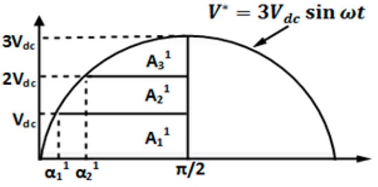
Figure 9.
Reference voltage waveform with dummy conducting angles.
The generation of a step pulse wave in the DCLCHB inverter to meet the equivalent areas as A11, A21, and A31. Here, main conducting angles () are defined as the switching timing angles of step pulse waves in the DCLCHB inverter. Figure 10 represents the main conducting angles and the stepped output phase voltage of the seven-level DCLCHB inverter during the positive half cycle.
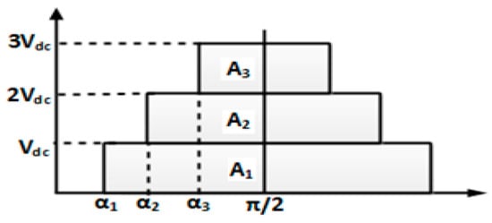
Figure 10.
Output phase-voltage of a seven-level DCLCHB inverter in the positive half-cycle voltage.
Assuming that the areas A1, A2, and A3 made by the main conducting angles in Figure 10 are equivalent to A11, A21, and A31 made by dummy conducting angles which are obtained as follows:
Area, A11 can be obtained from Equation (25):
A11 = (A11 + A21 + A31) − (A21 + A31)
Therefore, from Equation (25), A11 can be written as:
Since A11 is equal to A1, the real conducting angle of the proposed SPWCAD technique is obtained as,
Similarly, by equating A21 to A2, the angle can be expressed as,
can be obtained by equating A31 to A3 or by using Equation (30):
For a seven-level DCLCHB inverter, the conducting angles are calculated by using Equations (31)–(33).
Therefore, for a seven-level stepped waveform using the SPWCAD technique, three main conducting angles need to determined using Equations (31)–(33), i.e., and their values are 9.43°, 29.59°, and 55.88°, respectively, for the Mi = 0.8.
5.3. Comparison of the SPWCAD and EPCAD Technique
The conducting angles acquired by the SPWCAD technique are different from those acquired by the EPCAD technique. In the SPWCAD technique, conducting angles are acquired based on the modulation index (Mi) whereas the EPCAD technique gives the same conducting angles irrespective of the Mi. The proposed SPWCAD technique method can be applied to different modulation indices. The range of Mi and the number of conducting angles are listed in Table 4. Also, the values of conducting angles for the proposed SPWCAD technique using various modulation indices are listed in Table 5 for the DCLCHB inverter.
Table 4.
Number of conducting angles and steps in output waveform SPWCAD technique for various Mi.
Table 5.
Conducting angles of SPWCAD technique for various Mi.
5.4. THD Calculation of the Seven-Level Stepped Output Phase Voltage using CAD Techniques
The general THD expression for a periodic output phase voltage for a proposed DCLCHB inverter can be expressed as,
where V1 is the RMS (root mean square) value of the fundamental component and Vrms is the RMS value of the output phase voltage. For the proposed seven-level RV MLI, Vrms and V1 can be obtained by using Equations (35) and (36).
The output phase voltage THD expression for the proposed seven-level DCLCHB inverter can be obtained by substituting Equations (35) and (36) into Equation (34) and is given by:
Theoretical values of the output phase voltage THD for the seven-level DCLCHB inverter using EPCAD and the proposed SPWCAD techniques with the corresponding main conducting angles are given in Table 6.
Table 6.
Conducting angles, theoretical output phase voltage THD, and Vrms values for a seven-level DCLCHB inverter (m = 7).
6. Simulation and Experimental Validation of the Proposed TLBDCLCHB Inverter System
The simulation of the proposed single-phase seven-level TLBDCLCHB inverter system is analyzed using MATLAB Simulink and validated experimentally through FPGA-based pulse generation.
6.1. TLBC Simulation Results in Open-Loop Mode
The simulation of the TLBC is carried out and analyzed in open-loop mode by considering the DC input voltage Vdc of 50 V, which should be boosted to a total DC-link voltage of 250 V, 300 V, and 375 V for the duty cycles of 0.4, 0.5, and 0.6, respectively, and the voltage across each of the capacitors at the output should be boosted to 83.33 V, 100 V, and 125 V for the duty cycles of 0.4, 0.5, and 0.6, respectively, as shown in Figure 11, Figure 12 and Figure 13.
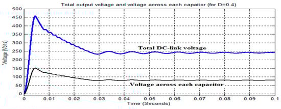
Figure 11.
Output of TLBC in open-loop for D = 0.4.
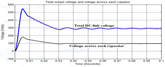
Figure 12.
Output of TLBC in open-loop for D = 0.5.
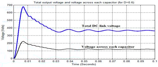
Figure 13.
Output of TLBC in open-loop for D = 0.6.
From Figure 11, Figure 12 and Figure 13, it is observed that the total DC-link output voltage for the duty cycles of 0.4, 0.5, and 0.6 has been boosted to 242.6, 291.4 V, and 361.4 V as opposed to 250 V, 300 V, and 375 V, respectively, due to the voltage drop across the switch and diodes. Similarly, the voltage drops across each of the capacitors are boosted to 82.17 V, 98.5 V, and 121.8 V as opposed to 83.33 V, 100 V, and 125 V. Also, it is noticed that the ripple in the total DC-link output voltage and voltage across each capacitor are increased by increasing the duty cycle from 0.4 to 0.6 to achieve the maximum DC-link output voltage with minimum ripple. Further, the open-loop mode of TLBC is extended to operate in closed-loop mode to maintain the required amount of DC-link output voltage by compensating the voltage drop across the switch and diodes, and, also, to reduce the ripple.
6.2. TLBC Simulation Results in Closed-Loop Mode
The proposed TLBC is implemented in closed-loop to maintain the constant output voltage using the voltage control loop. Here, the output of TLBC is measured and fed to an integral controller by comparing with the required reference output voltage to vary the duty cycle. Figure 14 shows the total DC-link output voltage and the voltage across each capacitor of the TLBC in closed-loop mode for D = 0.5. The corresponding change in duty cycle due to the reference output voltage is shown in Figure 15.
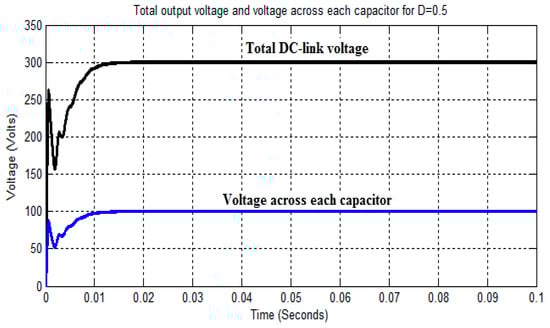
Figure 14.
Output of TLBC in closed-loop for D = 0.5.
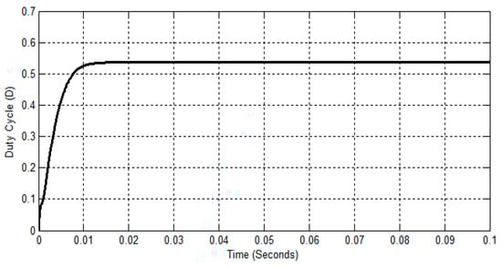
Figure 15.
Change in duty cycle of TLBC in closed-loop.
6.3. TLBDCLCHB Inverter Output using CAD Techniques
Simulation results of TLBC-fed DCLCHB inverter to generate a seven-level stepped output waveform using EPCAD and SPWCAD techniques and its THD analysis are shown in Figure 16, Figure 17, Figure 18, Figure 19, Figure 20 and Figure 21 for D = 0.5.
Figure 16.
Inverter output across LGU using the EPCAD technique.
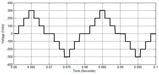
Figure 17.
TLBDCLCHB inverter output using EPCAD technique.
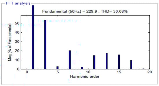
Figure 18.
THD analysis of TLBDCLCHB inverter output using EPCAD technique.
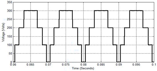
Figure 19.
Inverter output across LGU using the SPWCAD technique.
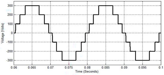
Figure 20.
TLBDCLCHB inverter output using the SPWCAD technique.
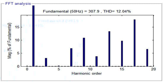
Figure 21.
THD analysis of the TLBDCLCHB inverter output using the SWPCAD technique.
6.3.1. Using the EPCAD Technique
Figure 16 shows the output voltage across the LGU in the DCLCHB inverter. Referring to Figure 16, the LGU generates a unipolar stepped waveform, and it can be converted to a bipolar stepped wave using PSGU. Figure 17 and Figure 18 show the seven-level stepped output phase voltage and its THD analysis of the TLBDCLCHB inverter using the EPCAD technique for the duty cycle of 0.5. It is observed that the magnitude of the fundamental output phase voltage and its RMS value is 229.9 V and 162.5 V, respectively. Also, the THD of the proposed TLBDCLCHB inverter output using the EPCAD technique is 30.08%.
6.3.2. Using the SPWCAD Technique
The unipolar output phase voltage across the LGU in the DCLCHB inverter using the SPWCAD technique is shown in Figure 19. Figure 20 and Figure 21 show the seven-level stepped output phase voltage and its THD analysis of the TLBDCLCHB inverter using the SPWCAD technique for the duty cycle of 0.5 with Mi = 0.8. It is observed that the magnitude of the fundamental output phase voltage and its RMS value is 307.9 V and 217.7 V, respectively. Also, the THD of the proposed TLBDCLCHB inverter output using the SPWCAD technique is 12.04%.
6.4. Experimental Validation of the TLBDCLCHB Inverter System Using an FPGA-Based Pulse Generation
The model of the proposed TLBDCLCHB inverter system-fed R-load is implemented employing Xilinx Spartan FPGA-based pulse generation [19,20] to validate the Simulink results. The block diagram, Xilinx Spartan6 development board, and the prototype model of the TLBDCLCHB inverter system using an FPGA is shown in Figure 22, Figure 23 and Figure 24, respectively. It consists of TLBC, the DCLCHB inverter, a personal computer (PC), an FPGA controller, R-load, buffer circuit, optocoupler, and driver circuit. The output of TLBC-fed DCLCHB inverter using an FPGA controller is shown in Figure 25.
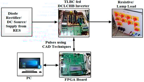
Figure 22.
Block diagram of the TLBDCLCHB hardware implementation.
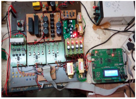
Figure 23.
Hardware implementation of the TLBDCLCHB inverter system with an FPGA controller.
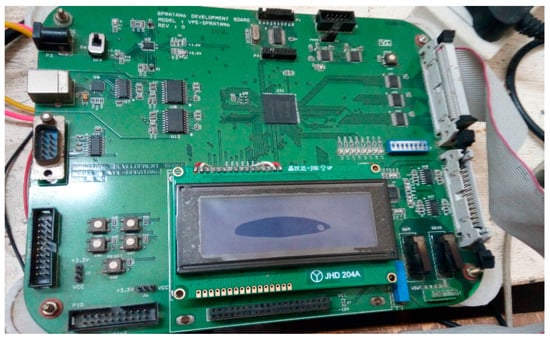
Figure 24.
Xilinx Spartan6 development board.
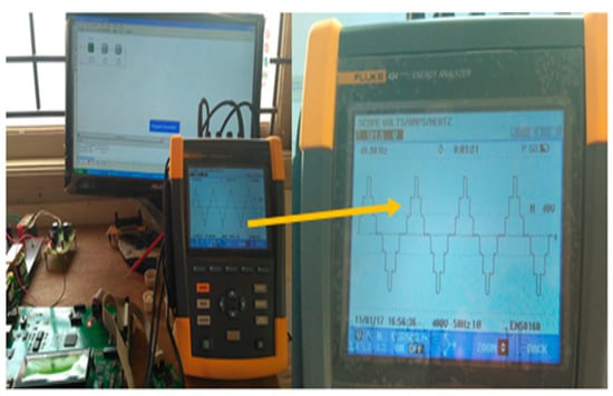
Figure 25.
Seven-level stepped output voltage of TLBC-fed DCLCHB inverter system.
Referring to Figure 26, the TLBC output voltage across each capacitor and the total DC-link voltage are shown in Channel 1 (CH1) and Channel (CH2), respectively, for D = 0.5. It is observed that CH1 and CH2 voltages are boosted to 100 V and 300 V, respectively.
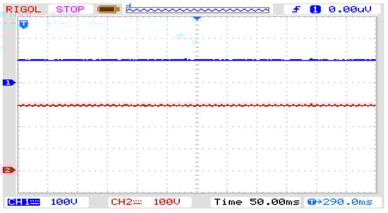
Figure 26.
Voltage across the capacitor CH1 and total DC-link voltage of TLBC CH2 for D = 0.5.
Figure 27 and Figure 28 show the generation of the pulse for the LGU switches (S1 to S6) in the DCLCHB inverter to generate the stepped output waveform using EPCAD and SPWCAD techniques, respectively, for the modulation index of 0.8. Figure 29 shows the generation of the pulse for the PSGU switches (P1 to P4) in the DCLCHB inverter to generate the positive and negative levels using an H-bridge inverter.
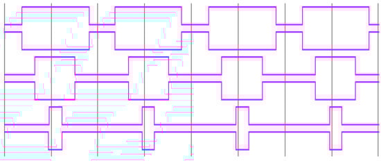
Figure 27.
Generation of pulses for the LGU switches (S1 to S6) in the DCLCHB inverter using the EPCAD technique through Xilinx ISE.
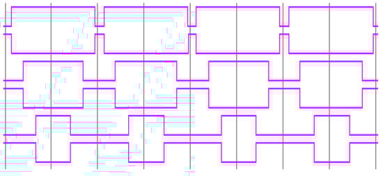
Figure 28.
Generation of pulses for the LGU switches (S1 to S6) in the DCLCHB inverter using the SPWCAD technique through Xilinx ISE.
Figure 29.
Generation of pulses for the PSGU switches (P1 to P4) in the DCLCHB inverter using a pulse generator through Xilinx ISE.
Figure 30 and Figure 31 represent the TLBDCLCHB inverter system experimental output phase voltage and its harmonic spectrum using the EPCAD technique for the generation of a seven-level stepped output voltage. Referring to Figure 30 and Figure 31, it is observed that the RMS value of the output phase voltage is 161.7 V and its THD is 31.5%.
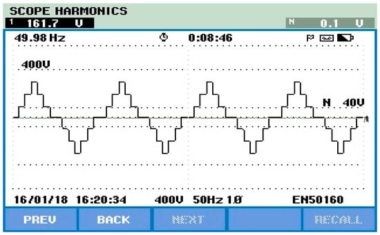
Figure 30.
TLBDCLCHB inverter output using the EPCAD technique.
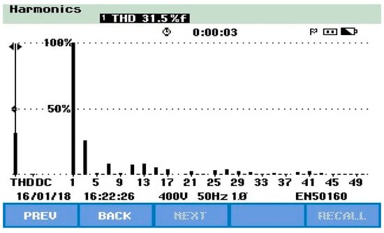
Figure 31.
THD analysis of the TLBDCLCHB inverter output using the EPCAD technique.
Figure 32 and Figure 33 represent the TLBDCLCHB inverter system experimental output phase voltage and its harmonic spectrum using the SPWCAD technique for the generation of a seven-level stepped output voltage. Referring to Figure 32 and Figure 33, it is observed that the RMS value of the output phase voltage is 216 V and its THD is 11.5%.
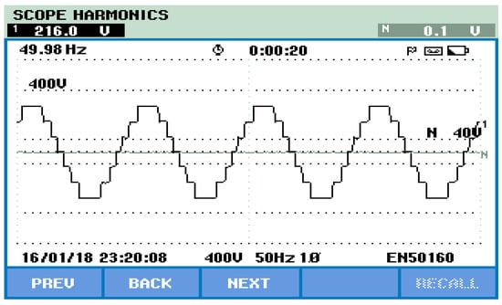
Figure 32.
TLBDCLCHB inverter output using the SPWCAD technique.
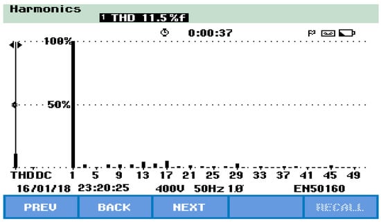
Figure 33.
THD analysis of the TLBDCLCHB inverter output using the SPWCAD technique.
6.5. TLBDCLCHB Inverter System Analysis and Comparison Using CAD Techniques
In this study, theoretical and simulation results of the proposed TLBDCLCHB inverter system for the generation of a seven-level stepped output phase voltage using the EPCAD and SPWCAD techniques have been validated experimentally through an FPGA-based pulse generation. Table 7 and Table 8 analyze the output phase voltage (Vrms) and THD of the TLBDCLCHB inverter system for different duty cycles, i.e., D = 0.4, 0.5, and 0.6. The THD of the prototype model for the proposed CAD techniques are conceded using a Fluke 435 power quality analyzer, and the results are presented in Figure 16, Figure 17, Figure 18, Figure 19, Figure 20, Figure 21, Figure 22, Figure 23, Figure 24, Figure 25, Figure 26, Figure 27, Figure 28 and Figure 29 for the EPCAD and SPWCAD techniques.
Table 7.
Simulation comparison of (Vrms) and % THD.
Table 8.
Experimental comparison of (Vrms) and %THD.
Referring to Table 6, Table 7 and Table 8, it is inferred that the most extreme output phase voltage and lower THD are accomplished by utilizing the SPWCAD technique rather than the EPCAD technique. From the simulation, it is obtained that Vrms and %THD content in the EPCAD technique are 161.7 V and 31% for D = 0.5. Whereas, in the case of the proposed SPWCAD technique, Vrms is 216 V and %THD is only 11.5% for D = 0.5 by considering Mi = 0.8. From the experimental results, it is observed that the Vrms and %THD content in the EPCAD technique are 161.7 V and 31% for D = 0.5. For the proposed SPWCAD technique, Vrms is 216 V and %THD is only 11.5% for D = 0.5 by considering Mi = 0.8. Therefore, theoretical values Vrms and %THD shown in Table 6 are validated with the simulation and experimental results with a tolerable error of ±2%. From the analysis, it is noticed that the magnitude of Vrms varies with respect to the duty cycle, but there is only a slight deviation in THD from 0.4 to 0.6.
7. Conclusions
In this paper, a TLBC-fed DCLCHB inverter system has been suggested to generate a seven-level stepped output phase voltage using a single DC source for better performance, efficiency, and reduced cost and size of the inverter. It also presented two control techniques for the DCLCHB inverter based on conducting angle determination, namely, EPCAD and SPWCAD techniques. Here, the SPWCAD technique gives the most extreme output phase voltage and lower THD compared to the EPCAD technique but the SPWCAD technique involves several trigonometric functions. However, same trigonometric functions are repeated; therefore, it is easy to acquire the conducting angles once the equations are derived based on the volt-second balance. In addition, TLBC has been suggested to achieve auto voltage balance and high voltage gain. Therefore, upon considering all the advantages, the proposed TLBDCLCHB inverter system is a good alternative for PV applications compared to the conventional boost-based MLI systems.
Author Contributions
A.K.D.V. and S.B.Ch. contributed to the main idea of this article. N.R.S. developed the Simulink model and performed the experiments, N.R.S., A.K.D.V. and S.B.Ch. all contributed to manuscript writing and revisions. All authors approved the final version to be published.
Funding
This research received no external funding.
Conflicts of Interest
The authors declare no conflict of interest.
Abbreviations
The following abbreviations are used in this manuscript:
| CAD | conducting angle determination |
| DCLCHB | DC-link cascade H-bridge |
| EPCAD | equal-phase CAD |
| LGU | level generation unit |
| THD | total harmonic distortion |
| TLBC | three-level boost converter |
| TLBDCLCHB | three-level boost DC-link cascade H-bridge |
| MLI | multilevel inverter |
| PSGU | phase sequence generation unit |
| PWM | pulse width modulation |
| PV | photovoltaic |
| SPWCAD | step pulse wave CAD |
References
- Rodriguez, J.; Lai, J.S.; Peng, F.Z. Multilevel inverters: A survey of topologies, controls, and applications. IEEE Trans. Ind. Electron. 2002, 49, 724–738. [Google Scholar] [CrossRef]
- Kjaer, S.B.; Pedersen, J.K.; Blaabjerg, F. A review of single-phase grid-connected inverters for photovoltaic modules. IEEE Trans. Ind. Appl. 2005, 41, 1292–1306. [Google Scholar] [CrossRef]
- Rodríguez, J.; Bernet, S.; Wu, B.; Pontt, J.O.; Kouro, S. Multilevel voltage-source-converter topologies for industrial medium-voltage drives. IEEE Trans. Ind. Electron. 2007, 54, 2930–2945. [Google Scholar] [CrossRef]
- Najafi, E.; Yatim, A.H. Design and implementation of a new multilevel inverter topology. IEEE Trans. Ind. Electron. 2012, 59, 4148–4154. [Google Scholar] [CrossRef]
- Davari, P.; Yang, Y.; Zare, F.; Blaabjerg, F. A review of electronic inductor technique for power factor correction in three-phase adjustable speed drives. In Proceedings of the 2016 IEEE Energy Conversion Congress and Exposition (ECCE), Milwaukee, WI, USA, 18–22 September 2016; pp. 1–8. [Google Scholar]
- Klumper, C.; Blaabjerg, F.; Thøgersen, P. Alternate ASDs: Evaluation of the converter topologies suited for integrated motor drives. IEEE Ind. Appl. Mag. 2006, 12, 71–83. [Google Scholar] [CrossRef]
- Su, G.J. Multilevel DC-link inverter. IEEE Trans. Ind. Appl. 2005, 41, 848–854. [Google Scholar] [CrossRef]
- Rao, S.N.; Kumar, D.A.; Babu, C.S. New multilevel inverter topology with reduced number of switches using advanced modulation strategies. In Proceedings of the 2013 International Conference on Power, Energy and Control (ICPEC), Sri Rangalatchum Dindigul, India, 6–8 February 2013; pp. 693–699. [Google Scholar]
- Uthirasamy, R.; Chinnaiyan, V.K.; Ragupathy, U.S.; Karpagam, J. Investigation on three-phase seven-level cascaded DC-link converter using carrier level shifted modulation schemes for solar PV system applications. IET Renew. Power Gener. 2017, 12, 439–449. [Google Scholar] [CrossRef]
- Prabaharan, N.; Palanisamy, K. A comprehensive review on reduced switch multilevel inverter topologies, modulation techniques and applications. Renew. Sustain. Energy Rev. 2017, 76, 1248–1482. [Google Scholar] [CrossRef]
- Luo, F.L. Investigation on best switching angles to obtain lowest THD for multilevel DC/AC inverters. In Proceedings of the 2013 IEEE 8th Conference on Industrial Electronics and Applications (ICIEA), Melbourne, Australia, 19–21 June 2013; pp. 1814–1818. [Google Scholar]
- Kang, D.W.; Kim, H.C.; Kim, T.J.; Hyun, D.S. A simple method for acquiring the conducting angle in a multilevel cascaded inverter using step pulse waves. IEE Proc.-Electr. Power Appl. 2005, 152, 103–111. [Google Scholar] [CrossRef]
- Rao, S.N.; Kumar, D.A.; Babu, C.S. Implementation of Multilevel Boost DC-Link Cascade based Reversing Voltage Inverter for Low THD Operation. J. Electr. Eng. Technol. 2018, 13, 1527–1537. [Google Scholar]
- Uthirasamy, R.; Ragupathy, U.S.; Chinnaiyan, V.K. Structure of boost DC-link cascaded multilevel inverter for uninterrupted power supply applications. IET Power Electron. 2015, 8, 2085–2096. [Google Scholar] [CrossRef]
- Prasad, G.D.; Jegathesan, V.; Moorthy, V. Minimization of power loss in newfangled cascaded H-bridge multilevel inverter using in-phase disposition PWM and wavelet transform based fault diagnosis. Ain Shams Eng. J. 2016. [Google Scholar] [CrossRef]
- Rosas-Caro, J.C.; Ramírez, J.M.; García-Vite, P.M. Novel DC-DC multilevel boost converter. In Proceedings of the 2008 IEEE Power Electronics Specialists Conference, Rhodes, Greece, 15–19 June 2008; pp. 2146–2151. [Google Scholar]
- Rosas-Caro, J.C.; Ramirez, J.M.; Valderrabano, A. Voltage balancing in DC/DC multilevel boost converters. In Proceedings of the 2008 40th North American Power Symposium, Calgary, AB, Canada, 28–30 September 2008; pp. 1–7. [Google Scholar]
- Rosas-Caro, J.C.; Ramirez, J.M.; Peng, F.Z.; Valderrabano, A. A DC–DC multilevel boost converter. IET Power Electron. 2010, 3, 129–137. [Google Scholar] [CrossRef]
- Maruthupandi, P.; Devarajan, N.; Sebasthirani, K.; Jose, J.K. Optimum control of total harmonic distortion in field programmable gate array-based cascaded multilevel inverter. J. Vib. Control 2015, 21, 1999–2005. [Google Scholar] [CrossRef]
- Cong, J.; Liu, B.; Neuendorffer, S.; Noguera, J.; Vissers, K.; Zhang, Z. High-level synthesis for FPGAs: From prototyping to deployment. IEEE Trans. Comput.-Aided Des. Integr. Circuits Syst. 2011, 30, 473–491. [Google Scholar] [CrossRef]
© 2018 by the authors. Licensee MDPI, Basel, Switzerland. This article is an open access article distributed under the terms and conditions of the Creative Commons Attribution (CC BY) license (http://creativecommons.org/licenses/by/4.0/).