Abstract
Fifth-Generation (5G) communication systems necessitate highly integrated technologies to facilitate ultra-fast data rates, low latency, and compact system configurations. The realization of these objectives depends on the advancement of packaging techniques, such as System-on-Package (SoP), wherein low-loss build-up layers play a vital role in enhancing signal transmission. In this context, the electrical characterization of a 25 μm thick SUEX dielectric material used as a build-up layer for SoP applications is presented. Various test structures, including microstrip ring resonators (MRRs), coplanar waveguides (CPWs), and microstrip lines (MSs), are fabricated and measured over a frequency range of 1–30 GHz. The electrical properties are extracted using MRRs, whereas CPW and MS line structures are utilized for characterization and validation. The measurement results indicate that while the average dielectric constant of the SUEX dry film ranges from 3.07 to 3.10, the corresponding loss tangent varies between 5.75 × 10⁻³ and 5.83 × 10⁻³ across a frequency range of 10.28–27.47 GHz. These results verify that SUEX has low-loss properties, making it a suitable dielectric for build-up layers in SoP modules, where reducing signal loss is crucial for 5G and future communication technologies.
1. Introduction
As the world rapidly advances in digital technology, 5G has become a key part of modern communication networks. It offers unmatched improvements in data speeds, extremely low latency, and the ability to connect a large number of devices [1]. These advances facilitate groundbreaking uses in industrial automation, autonomous transportation, smart city development, and the Internet of Things (IoT), fostering a highly connected and intelligent ecosystem [2].
The 5G spectrum is classified into low-band (<1 GHz), mid-band (1–6 GHz), and high-band (>24 GHz). Shifting the carrier frequency from the low band to the high band imposes significant constraints due to elevated signal losses. To overcome these challenges, advanced packaging, which integrates multiple electronic devices into a single module, is required. System-on-Chip (SoC) and SoP, as techniques of advanced packaging, enable highly integrated electronic systems and play a crucial role in enhancing performance, power efficiency, and miniaturization [3]. SoC integration includes combining numerous functional components, such as processing units, memory, analog/digital circuitry, and communication interfaces, onto a single die [4]. However, it suffers from high development costs, complex design methodologies, and extensive verification processes. SoP technology is a complementary method that integrates heterogeneous circuits (e.g., logic, RF, power management, and photonics) within a single package [5]. SoP has the advantage of being low-cost, easy to implement, and highly stable. Table 1 presents the trade-off between SoC and SoP technologies.
Table 1.
SoP/SoC trade-off diagram.
SoP technology consists of an interposer, build-up layers, redistribution layers (RDLs), and interconnections, as shown in Figure 1. An interposer layer serves as an intermediate layer and provides mechanical support to bring chips together. Interconnections and RDLs in build-up layers are employed to reroute signals between active and passive devices. Thus, selecting an appropriate build-up material is essential for electrical performance, thickness control, and fabrication costs. Liquid-based materials such as liquid crystal polymer (LCP), SU-8, polyimides, and Benzo-cyclobutene (BCB) are organic materials that may be candidates for the build-up layers [6,7,8]. However, they struggle to achieve thicknesses above 40 μm and encounter difficulties at high curing temperatures. On the other hand, dry-film dielectric materials have emerged as a strong choice due to their outstanding process control, high-resolution patterning, and compatibility with packaging techniques. They offer several advantages, including low-temperature processing, improved adhesion to semiconductor substrates, and enhanced uniformity [9]. Anjinomoto Build-up Film (ABF), Alumina Ribbon Ceramic (ARC), and ZEONIF ZS-100 are dry films reported in the literature. In previous studies [10], an ABF/glass/ABF-based stack-up was characterized from 20 to 170 GHz. Also, different test structures were designed on an ARC material to extract the electrical properties and loss performance of the transmission line [11]. In addition, low-pass filters were fabricated by using spiral inductors and parallel-plate stitched capacitors on a glass-based ZS-100 build-up layer [12]. However, these dry films are not photo-imageable, so they require an additional device to etch them. Additionally, commercially available dry film photoresist series, such as WBR, WB, MX, ADEX, and DF, exhibit limited flexibility in achievable thickness ranges [13,14]. To address the limitations above, DJ-MICROLAMINATES introduces an innovative epoxy-based thin-dry-film photoresist, SUEX. SUEX exhibits glass-transition temperature (Tg: 173 °C), water absorption (%1.5/h), and Coefficient of Thermal Expansion (CTE) (50). Furthermore, following the curing process at 200 °C for 30 min, the measured dielectric constant and loss tangent are 3.2 and 0.0032, respectively. Additionally, it has strong adhesion to semiconductor surfaces and metal surfaces. Available thicknesses range from 5 µm to 1 mm for circular and square sheets [15]. The material properties are provided in Table 2. However, a comprehensive investigation of the electrical properties of SUEX remains absent from the existing literature.
Figure 1.
Schematic view of System-on-Package (SoP).
Table 2.
Material properties of SUEX [15].
Accordingly, in this article, we present, for the first time in the literature, the electrical characterizations of SUEX dry film as a build-up layer over a frequency range of up to 30 GHz. In addition, the dB/mm insertion loss of CPWs on stack and MSs is evaluated. Several test structures are designed and fabricated to analyze the performance of the SUEX dry film as a build-up layer. Finally, the fabricated test structures were measured to validate the reliability of the proposed design and fabrication methodologies. The presented results show that SUEX can be regarded as an alternative build-up layer for SoP modules. This article is organized as follows: Section 2 explains the test structure design and fabrication process. Section 3 presents the calculation of the electrical properties of the SUEX dry film and a comparison of simulation and measurement results.
2. Design and Fabrication of Test Structures
In this part of the article, the design of the test structure and fabrication methods are explained in detail. Also, the design and validation flow chart is illustrated in Figure 2. The process begins with the design of the test structures. This is followed by fabricating the structures and extracting the material’s electrical properties. Finally, full-wave electromagnetic simulations are performed. The results are confirmed by comparing them with experimental measurements.
Figure 2.
Design and validation flow chart.
2.1. Microstrip Ring Resonators
MRRs are frequently utilized to determine the dielectric constant and loss tangent of materials [16]. Their advantages include the ability to deliver accurate results, ease of wafer-level manufacturing, and low cost. The resonance frequencies of MRRs are the consequence of the material’s dielectric constant. MRRs are designed considering the fundamental frequency of operation using
where , , , and denote resonance frequency, speed of light in vacuum, mean ring radius, and effective permittivity, respectively. In order to obtain the dielectric constant of SUEX (), MRRs with different radii with resonances of 10, 20, and 27 GHz are designed, as shown Figure 3a. Both ends of MRRs begin with grounded coplanar waveguide (GCPW) probe pads and then turn into a microstrip line. In addition, 60° circles are inserted at the end of the microstrip line to obtain better coupling efficiency. Additionally, 25 μm diameter microvias are inserted to enhance coupling from the ground pads to the ground plane. The dimensions of the MRRs are given in Table 3.
Figure 3.
Designed test devices. (a) MRR. (b) MS. (c,d) Side and top view of UCPW on stack. (e,f) Side and top view of GCPW on SUEX.
Table 3.
Dimensions of designed and fabricated structures.
2.2. Microstrip Line
A microstrip transmission line is a planar guided-wave configuration comprising a narrow metallic conductor strip on the upper surface of a dielectric substrate, with a continuous ground plane on the opposite side, as illustrated in Figure 3b. To evaluate its performance, a 50 Ω microstrip line is designed on SUEX in a frequency range of 1–30 GHz. GCPW-to-microstrip transitions are implemented at both ends of the microstrip line to facilitate accurate and repeatable probe landings during on-wafer measurements. The dimensions of the MS line are given in Table 3.
2.3. CPW Transmission Lines
The CPW transmission line in the build-up layer transmits a signal from one point to another. For this reason, an ungrounded coplanar waveguide UCPW on silicon–SUEX stacks and a GCPW on SUEX are designed to characterize their performance. The designed structures are shown in Figure 3c–f. Their characteristic impedances are set to 50 Ω. The signal line width and signal–ground space are adjusted to be compatible with a 200 μm probe pitch spacing. The dimensions of CPWs are given in Table 3.
2.4. Fabrication Process
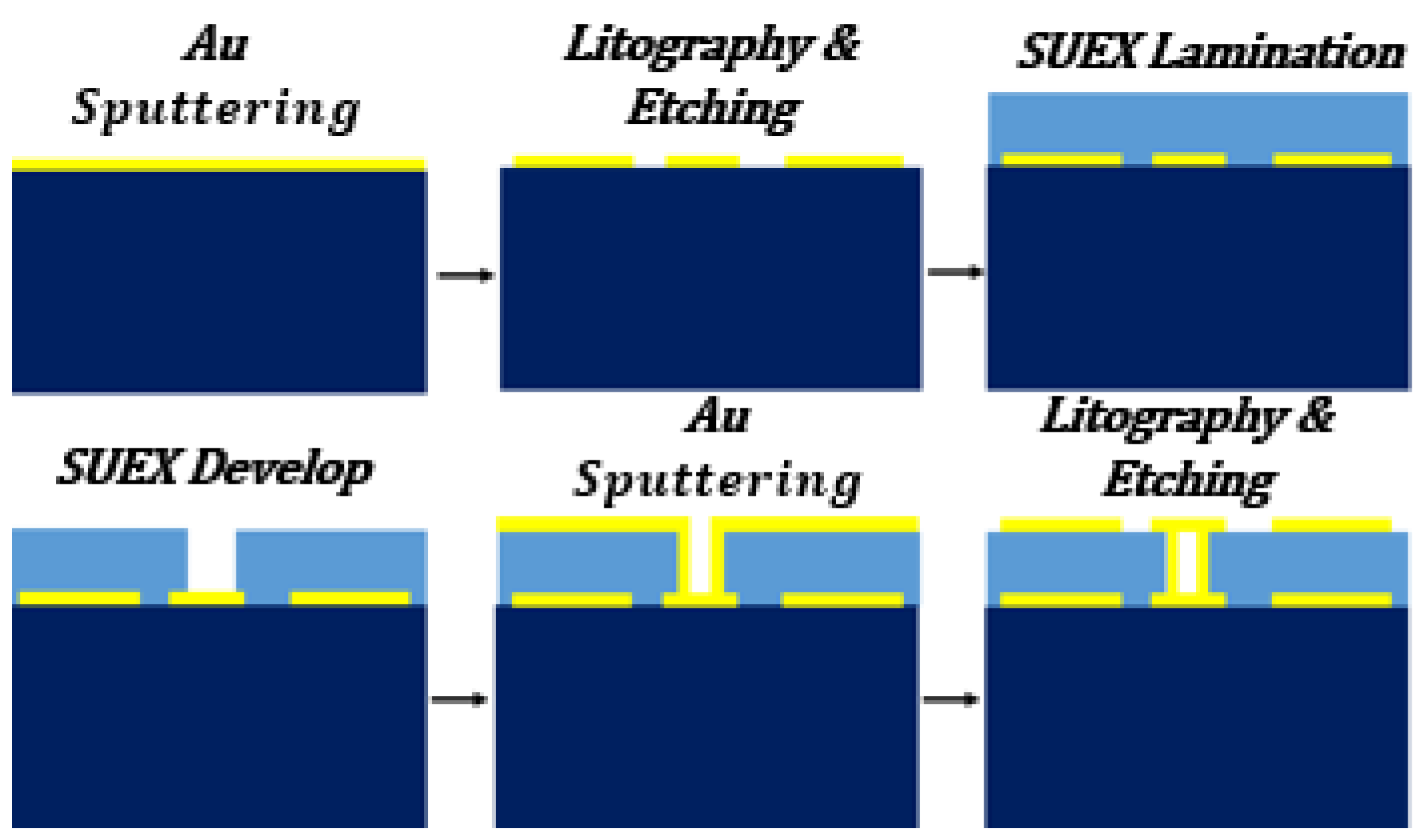
The fabrication process involves a sequence of microfabrication steps including sputtering, lithography, lamination, development, and wet etching, as illustrated in Figure 4. Initially, a dehydration bake is performed on the silicon wafer to remove contamination and moisture. Then, a bilayer stack consisting of Cr/Au (20/250 nm) metal layers is deposited using AJA sputtering systems, and the metal stack is etched to create devices on a silicon wafer. A mask exposure and development process is performed to open the microvias, followed by lamination of the SUEX dry film on the silicon substrate. The lamination process is carried out at a temperature of 70 °C with a speed of 1 ft/min. An O2 plasma treatment process is subsequently performed to remove surface residues. A second Cr/Au (20/1300 nm) metal layer stack is deposited onto the SUEX film to form the upper metallization layer. The lithography and wet etching steps are completed, leading to the formation of the final structures. The electrical conductivity of the metal layer is measured to be approximately S/m using the MAGNETRON resistance measurement system. The fabricated test structures, including MRR, MS, UCPW-on-stack, and GCPW, are shown in Figure 5. Furthermore, the dimensions of the fabricated devices are measured using an optical microscope. The measured widths of the MRR, CPW, and GCPW lines were found to be %1–5 smaller than their designed values. In addition, the gap between the signal and ground planes in the CPW structures was %1–5 larger than that of the modeled devices. These dimensional deviations lead to an estimated impedance variation of approximately 2–3 Ω in the given frequency range.
Figure 4.
Fabrication steps of designed structures.
Figure 5.
Fabricated devices. (a) MRR. (b) MS. (c) UCPW on stack. (d) GCPW on SUEX.
3. Characterization Results and Comparison
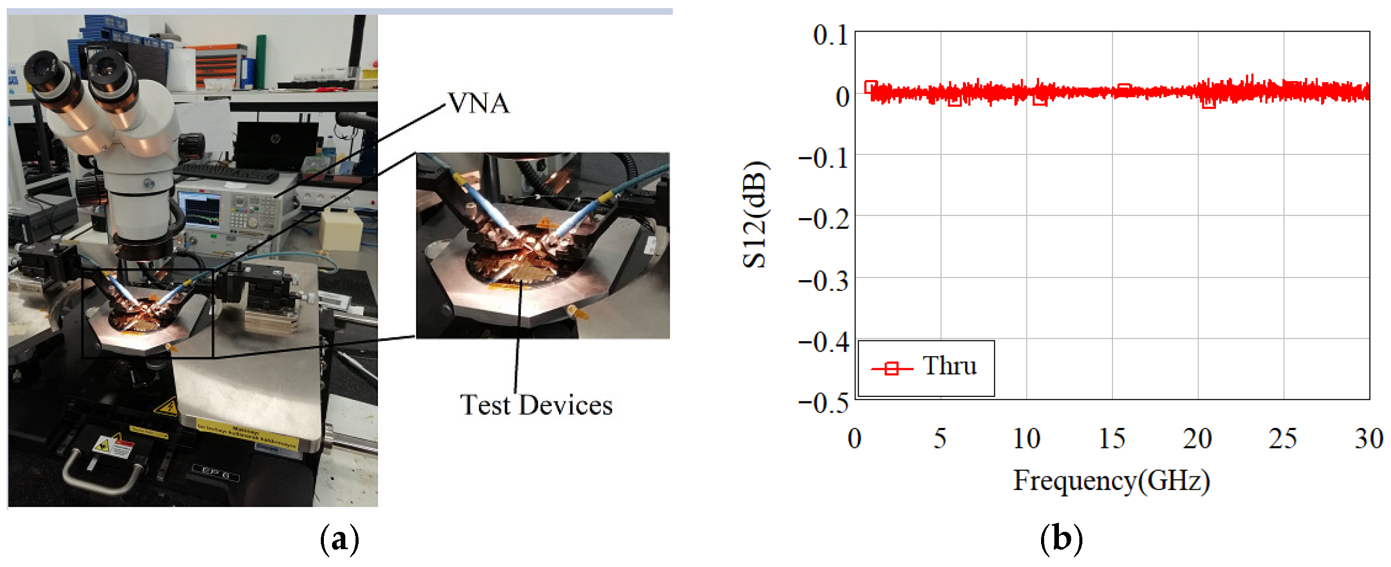
The measurement of the fabricated test structures is performed using a Keysight Vector Network Analyzer (VNA) operating over 1–30 GHz, as illustrated in Figure 6a. A ground–signal–ground (GSG) probe with a 200 µm pitch spacing, provided by Formfactor, is considered for conducting measurements. Before the measurement, short-open-load-through (SOLT) calibration is performed using a Pico-probe CS-9 calibration substrate to de-embed the effects of the probe pads, cable loss, and systematic errors arising from the VNA and probe system. The measurement result of the Thru standard after SOLT calibration is illustrated in Figure 6b. The measured transmission coefficient varies by only 0.02 dB across the evaluated frequency range, indicating excellent calibration accuracy and port matching.
Figure 6.
(a) Measurement setup. (b) The result of the Thru standard after SOLT calibration.
3.1. Characterization of Electrical Properties of SUEX
MRRs with various radii are fabricated to extract the frequency-dependent dielectric constant and loss tangent of SUEX dry film. A quasi-static model is employed to accurately determine the material’s dielectric constant. Firstly, the effective dielectric constant is estimated depending on the corresponding resonant frequency. Then, the relative permittivity of SUEX is derived as [17]
where is the SUEX dry film thickness, is the microstrip line thickness, is the microstrip line width, and is the SUEX dry film dielectric constant. The extracted dielectric constant within the 10.28–27.47 GHz frequency range varied between 3.14 and 3.19. In addition to the quasi-static model, the trial-and-error method is used to extract both the dielectric constant and the loss tangent. In this approach, the dielectric constant and loss tangent are iteratively tuned in the simulation until the simulated resonant frequency and insertion loss closely match the measured values. Depending on the method, the extracted dielectric constant of the SUEX dry film ranged from 2.89 to 3.02 across 10.28–27.47 GHz, which is approximately 7–8% lower than the values obtained by the quasi-static model. The observed discrepancy can be attributed to several factors, including the quality factor (Q-factor) of the ring resonator, minor calibration uncertainties, and deviations in the mean resonator radius. The modeling results indicate that a 50 µm variation in the mean radius of the microstrip ring resonator corresponds to an approximately 1.5–2% change in the extracted dielectric constant. Moreover, the quasi-static model neglects dispersion effects, which may further contribute to the observed deviation [17]. Furthermore, a previous study [18] reported that using different extraction methods to determine the material’s electrical properties can lead to variations exceeding 8%. Overall, variation between the given methods is considered negligible for practical dielectric characterization and remains within acceptable experimental uncertainty limits.
A detailed comparison of the extracted dielectric constant values is provided in Table 4, along with the corresponding average values obtained from the quasi-static and trial-and-error methods. Additionally, the frequency-dependent variation in the average dielectric constant of the SUEX dry film is shown in Figure 7a. The discrepancy between the average and individually calculated dielectric constants ranges from approximately 2.2% to 3.7%, which is within an acceptable margin for material characterization. This level of variation highlights the consistency of the extraction techniques and confirms the reliability of the proposed methods for evaluating the electrical properties of the SUEX material.
Table 4.
Extracted dielectric constant and loss tangent of SUEX.
Figure 7.
(a) Extracted dielectric constant and loss tangent of the SUEX dry film. (b) Measurement and simulation results of MRRs with 10, 20, and 27 GHz resonance frequency.
The extracted loss tangent of the SUEX film is observed to be between 6 × 10⁻³ and 6.1 × 10⁻³ within the frequency range of 20.93–27.47 GHz, indicating an acceptable loss tangent. The absence of a reliable loss tangent at 10.28 GHz can be attributed to the fact that, at this frequency, the skin depth is much larger than the metal thickness, resulting in reduced electromagnetic field confinement and less accurate attenuation extraction. Additionally, minor calibration deviations and weak coupling between the ground planes may have further contributed to the measurement inconsistency.
In addition to the MRR method, the UCPW transmission line method is also followed to obtain the loss tangent of SUEX material. Figure 3c shows the cross-sectional view of the UCPW transmission line structure. In this design, SUEX thin film is characterized by a thickness of and is laminated on a silicon substrate with a thickness of . In the transmission line method, a complex propagation constant () is evaluated from the ABCD matrix, which is transformed from the measured scattering matrix [18]. The conversions from two-port network parameters to the transmission matrix are described in (3)–(7). Following the conversion, the total attenuation constant () and effective dielectric constant of stack () can be calculated using (8) and (9). is the characteristic impedance, which is assumed to be 50 Ω, and correspond to the scattering parameters.
Accurate determination of conductor loss is essential to precisely extracting the loss tangent of the SUEX material. While several methods have been reported in the literature for determining conductor losses, many assume that the metal thickness exceeds three to five times the skin depth, which does not hold in our case [19,20]. Thus, conductor () and radiation loss () are estimated through full-wave electromagnetic simulation in which the loss tangent of SUEX is set to zero. Following the given approach, effective loss tangent of stack () is extracted using
Finally, the conformal mapping method is used to extract the loss tangent of SUEX as follows [21]:
where , , and denote the filling factor, dielectric constant of SUEX, dielectric constant of silicon, loss tangent of SUEX, and loss tangent of silicon, respectively. Silicon is assumed to be lossless since it possesses high resistivity (>20 kΩ/cm). and are the elliptical integral of first kind and its complement. In order to extract the loss tangent, UCPW transmission lines with a length of 3000 and 4000 are utilized as test structures, and their detailed results are given in Table 4. Average loss tangent of SUEX vary between – as plotted in Figure 7a. Within the given frequency range, a deviation of approximately % 1.7–5.3 is observed between the test structures, reflecting acceptable variation for high-frequency electrical characterization.
To further validate the accuracy of the extracted dielectric properties, the average loss tangent and dielectric constant of the SUEX film are simulated using MRR in the Finite Element Method (FEM)-based commercial solver ANSYS HFSS v21. Simulated and measured MRR results are given in Figure 7b. According to the results, the simulated resonance frequency of each MRR closely match the measured resonance. Moreover, insertion loss values at each resonance point show minimal variation, indicating high consistency across the frequency range. Minor differences can be attributed to calibration and fabrication errors.
3.2. Microstrip Line Characterization
Figure 8 illustrates the measured scattering parameters of the microstrip transmission line obtained after performing a SOLT calibration. It is essential to note that the measurement configuration includes GCPW-to-microstrip transition sections at both ends of the line. However, since these transition segments are electrically short and designed with a characteristic impedance of 50 Ω, their contribution to the measured S-parameters of the microstrip line is negligible. Figure 8a presents the measured scattering parameters of the microstrip line with a total length of 1.7 mm. The observed reflection coefficient S11 remains below –15 dB across the measured frequency range, confirming good impedance matching between the line and the measurement system. Furthermore, the extracted insertion loss per unit length (dB/mm) varies from approximately 0.13 to 0.45 dB/mm over the 1–30 GHz frequency range, as shown in Figure 8b, exhibiting excellent agreement with the corresponding simulation results.
Figure 8.
Scattering parameters of microstrip lines. (a) S11 and S12-measured results in dB for 1.7 mm long microstrip line. (b) Measured dB/mm insertion loss of microstrip lines versus simulated results.
3.3. CPW Line Characterization
Figure 9 shows the measured scattering parameters of UCPW in a frequency range of 1–30 GHz. Additionally, the S-parameter response of the 5 mm long UCPW line is shown in Figure 9a. Furthermore, the measured insertion loss per unit length (dB/mm) of UCPW varies from 0.034 to 0.25 dB within a frequency range of 1 to 30 GHz, as given in Figure 9b.
Figure 9.
Scattering parameters of UCPW lines. (a) S11 and S12-measured results in dB for 5 mm long UCPW line. (b) Measured dB/mm insertion loss of UCPW lines versus simulated results.
In addition to UCPW, the scattering parameters of the GCPW structures are also presented in Figure 10. Figure 10a shows the measured scattering parameters of the 5 mm long GCPW line. As observed, the reflection coefficient remains low over the entire frequency range, indicating good impedance matching between the line and the measurement system. The extracted insertion loss ranges from 0.08 to 0.4 dB/mm within a frequency range of 1 to 30 GHz. Furthermore, the UCPW lines are simulated using the extracted electrical properties of SUEX, demonstrating a strong correlation with the measurement results shown in Figure 10b.
Figure 10.
Scattering parameters of GCPW lines. (a) S11 and S12-measured results in dB for a 5 mm long GCPW. (b) Measured dB/mm insertion loss of GCPW line versus simulated results.
4. Comparison with Other Studies
Table 5 compares the dielectric constants, loss tangents and dB/mm insertion losses of SUEX with other dry film materials like Roger RT 5880, LTCC, ABF, ARC, and ZIF. It is important to emphasize that SUEX exhibits stable electrical properties across the operating frequency. Also, it offers a well-balanced combination of a low dielectric constant, a favorable loss tangent, and moderate insertion loss compared to the given materials. The results show that implementing build-up layers with SUEX and a practical approach for advanced packaging applications demands a low-loss build-up layer. Furthermore, due to the flexible thickness range and photo-imageability of SUEX dry film, costs and application complexity can be reduced.
Table 5.
Comparison of dielectric constant, loss tangent, and dB/mm insertion loss performance of SUEX dry film with other dry film materials.
5. Conclusions
In this article, we present the electrical characterization of SUEX material in a frequency range of 1–30 GHz using MRR and various transmission lines. The measured results demonstrate that SUEX exhibits a low dielectric constant (3.07–3.10) and low loss tangent (5.75 × 10⁻³–5.83 × 10⁻³) between 10.28 and 27.47 GHz, confirming its potential as a low-loss dielectric layer for System-on-Package (SoP) architectures in 5G communication systems. Also, it can be deployed at the panel level and in fan-out packaging platforms. Future research may focus on characterization of SUEX-based build-up layers for the V, W, D and sub-THz frequency bands. Furthermore, double-sided multilayer packaging configurations can be realized on silicon or glass interposers to improve antenna-in-package solutions for industry applications.
Author Contributions
S.D.: investigation, fabrication, measurement, writing, editing. S.E.: investigation, measurement, editing. N.O.: investigation, measurement, editing. K.E.: investigation, editing. M.U.: investigation, measurement, editing, resources, project administration, supervision. All authors have read and agreed to the published version of the manuscript.
Funding
This work was supported by ASELSAN Inc. and the Scientific and Technological Research Council of Turkey (TUBITAK) as a research project with grant number 122E142.
Data Availability Statement
Dataset is available on request from the authors.
Acknowledgments
The authors would like to thank ASELSAN, Inc. for their funding support. We also appreciate the METU-MEMS Research and Application Center personnel for their assistance with the fabrication process.
Conflicts of Interest
Saim Ekici and Nihan Oznazlı was employed by the company ASELSAN. The remaining authors declare that the research was conducted in the absence of any commercial or financial relationships that could be construed as a potential conflict of interest.
References
- Seker, C.; Güneser, M.T.; Ozturk, T. A Review of Millimeter Wave Communication for 5G. In Proceedings of the 2018 2nd International Symposium on Multidisciplinary Studies and Innovative Technologies (ISMSIT), Ankara, Turkey, 19–21 October 2018. [Google Scholar]
- Loghin, D.; Cai, S.; Chen, G.; Dinh, T.T.A.; Fan, F.; Lin, Q.; Ng, J.; Ooi, B.C.; Sun, X.; Ta, Q.T.; et al. The Disruptions of 5G on Data-Driven Technologies and Applications. IEEE Trans. Knowl. Data Eng. 2020, 32, 1179–1198. [Google Scholar] [CrossRef]
- Božanić, M.; Sinha, S. Device Technologies and Circuits for 5G and 6G. In Mobile Communication Networks: 5G and a Vision of 6G; Božanić, M., Sinha, S., Eds.; Springer International Publishing: Cham, Switzerland, 2021; pp. 99–154. [Google Scholar]
- Dai, W.W.M. Historical Perspective of System in Package (SiP). IEEE Circuits Syst. Mag. 2016, 16, 50–61. [Google Scholar] [CrossRef]
- Tummala, R.R. Packaging: Past, present and future. In Proceedings of the 2005 6th International Conference on Electronic Packaging Technology, Shenzhen, China, 30 August–2 September 2005. [Google Scholar]
- Sahin, S.; Ghalichechian, N.; Sertel, K. Ultra-wideband, high-efficiency, on-chip mmW phased arrays with wafer-level vertical integration. In Proceedings of the 2014 USNC-URSI Radio Science Meeting (Joint with AP-S Symposium), Memphis, TN, USA, 6–11 July 2014. [Google Scholar]
- Zerounian, N.; Aouimeur, W.; Grimault-Jacquin, A.S.; Ducournau, G.; Gaquière, C.; Aniel, F. Coplanar waveguides on BCB measured up to 760 GHz. J. Electromagn. Waves Appl. 2021, 35, 2051–2061. [Google Scholar] [CrossRef]
- Thompson, D.C.; Tantot, O.; Jallageas, H.; Ponchak, G.E.; Tentzeris, M.M.; Papapolymerou, J. Characterization of liquid crystal polymer (LCP) material and transmission lines on LCP substrates from 30 to 110 GHz. IEEE Trans. Microw. Theory Tech. 2004, 52, 1343–1352. [Google Scholar] [CrossRef]
- Watanabe, A.O.; Ali, M.; Sayeed, S.Y.B.; Tummala, R.R.; Pulugurtha, M.R. A Review of 5G Front-End Systems Package Integration. IEEE Trans. Compon. Packag. Manuf. Technol. 2021, 11, 118–133. [Google Scholar] [CrossRef]
- Rehman, M.U.; Ravichandran, S.; Watanabe, A.O.; Erdogan, S.; Swaminathan, M. Characterization of ABF/Glass/ABF Substrates for mmWave Applications. IEEE Trans. Compon. Packag. Manuf. Technol. 2021, 11, 384–394. [Google Scholar] [CrossRef]
- Aslani-Amoli, N.; Rehman, M.u.; Liu, F.; Swaminathan, M.; Zhuang, C.G.; Zhelev, N.Z.; Seok, S.H.; Kim, C. Characterization of Alumina Ribbon Ceramic Substrates for 5G and mm-Wave Applications. IEEE Trans. Compon. Packag. Manuf. Technol. 2022, 12, 1432–1445. [Google Scholar] [CrossRef]
- Sato, Y.; Sitaraman, S.; Sukumaran, V.; Chou, B.; Min, J.; Ono, M.; Karoui, C.; Dosseul, F.; Nopper, C.; Swaminathan, M.; et al. Ultra-miniaturized and surface-mountable glass-based 3D IPAC packages for RF modules. In Proceedings of the 2013 IEEE 63rd Electronic Components and Technology Conference, Las Vegas, NV, USA, 28–31 May 2013. [Google Scholar]
- Available online: https://djmicrolaminates.com/ (accessed on 13 November 2025).
- Available online: https://www.dupont.com/electronics-industrial/dry-film-photoresists-wlp.html (accessed on 13 November 2025).
- Johnson, D.; Voigt, A.; Ahrens, G.; Dai, W. Thick epoxy resist sheets for MEMS manufactuing and packaging. In Proceedings of the 2010 IEEE 23rd International Conference on Micro Electro Mechanical Systems (MEMS), Hong Kong, China, 24–28 January 2010. [Google Scholar]
- Bernard, P.A.; Gautray, J.M. Measurement of dielectric constant using a microstrip ring resonator. IEEE Trans. Microw. Theory Tech. 1991, 39, 592–595. [Google Scholar] [CrossRef]
- Bahl, I.J.; Garg, R. Simple and accurate formulas for a microstrip with finite strip thickness. Proc. IEEE 1977, 65, 1611–1612. [Google Scholar] [CrossRef]
- Yang, R.-Y.; Su, Y.-K.; Weng, M.-H.; Hung, C.-Y.; Wu, H.-W. Characteristics of coplanar waveguide on lithium niobate crystals as a microwave substrate. J. Appl. Phys. 2007, 101, 014101. [Google Scholar] [CrossRef]
- Heinola, J.M.; Tolsa, K. Dielectric characterization of printed wiring board materials using ring resonator techniques: A comparison of calculation models. IEEE Trans. Dielectr. Electr. Insul. 2006, 13, 717–726. [Google Scholar] [CrossRef]
- Inder, B.; Maurizio, B.; Ramesh, G. Microstrip Lines and Slotlines, 3rd ed.; Artech: London, UK, 2013. [Google Scholar]
- Chen, T.C.; Wang, L.; Goodyear, G.; Yializis, A.; Xin, H. Broadband Microwave Characterization of Nanostructured Thin Film with Giant Dielectric Response. IEEE Trans. Microw. Theory Tech. 2015, 63, 3768–3774. [Google Scholar] [CrossRef]
- Fesharaki, F.; Djerafi, T.; Chaker, M.; Wu, K. Guided-Wave Properties of Mode-Selective Transmission Line. IEEE Access 2018, 6, 5379–5392. [Google Scholar] [CrossRef]
- Bray, J.R.; Kautio, K.T.; Roy, L. Characterization of an experimental ferrite LTCC tape system for microwave and millimeter-wave applications. IEEE Trans. Adv. Packag. 2004, 27, 558–565. [Google Scholar] [CrossRef]
- Khan, W.T.; Tong, J.; Sitaraman, S.; Sundaram, V.; Tummala, R.; Papapolymerou, J. Characterization of electrical properties of glass and transmission lines on thin glass up to 50 GHz. In Proceedings of the 2015 IEEE 65th Electronic Components and Technology Conference (ECTC), San Diego, CA, USA, 26–29 May 2015. [Google Scholar]
- Kang, S.M.; Kweon, H.; Park, S.; Bae, B.S. Low Dk/Df Siloxane Hybrid Laminates for Advanced Packaging Substrate. In Proceedings of the 2025 IEEE 75th Electronic Components and Technology Conference (ECTC), Dallas, TX, USA, 27–30 May 2025. [Google Scholar]
Disclaimer/Publisher’s Note: The statements, opinions and data contained in all publications are solely those of the individual author(s) and contributor(s) and not of MDPI and/or the editor(s). MDPI and/or the editor(s) disclaim responsibility for any injury to people or property resulting from any ideas, methods, instructions or products referred to in the content. |
© 2026 by the authors. Licensee MDPI, Basel, Switzerland. This article is an open access article distributed under the terms and conditions of the Creative Commons Attribution (CC BY) license.