Abstract
This work describes the design and experimental testing of a low-noise amplifier (LNA) fabricated on a printed circuit board (PCB) and operating near 2 GHz. The amplifier uses a discrete bipolar junction transistor (BJT) together with fully distributed microstrip matching networks without relying on lumped matching components. The main design goal is to obtain stable operation with low noise figure and moderate gain over a wide frequency range while keeping the circuit tolerant to layout parasitics and fabrication variations. Circuit-level simulations are performed using AWR Microwave Office and are followed by full-wave electromagnetic simulations in Sonnet Software to account for layout-dependent effects. A prototype is fabricated on a 60-mil Rogers RO4003C substrate and characterized through S-parameter, noise-figure, and linearity measurements. Measured results show a gain of approximately 13.84 ± 1 dB over the 1.75–2.25 GHz frequency range, with a minimum noise figure of 1.615 dB at 2 GHz. Stable operation is maintained across the entire band, and the measured 1 dB gain compression point is approximately 0.5 dBm. The results demonstrate that a fully distributed microstrip matching approach provides a practical and reproducible PCB-based LNA solution for sub-6-GHz receiver front-end applications.
1. Introduction
Low-noise amplifiers (LNAs) are key building blocks in radio-frequency (RF) receivers because they strongly effect the noise performance and sensitivity of the system [1]. Since the LNA is the first active stage in the receiver chain, its noise figure directly influences the overall receiver noise figure, as explained by Friis’ formula [2]. For this reason, low noise operation together with stable and predictable behavior is a basic requirement in RF front-end design [3]. In recent years, the growth of sub-6-GHz wireless systems, such as fifth-generation new radios (5G NR), wireless fidelity (Wi-Fi 6/6E/7), and Internet-of-Things (IoT) applications, increasing the need for LNAs that can operate over wider frequency ranges [4]. In these systems, LNAs are expected to provide low noise figure together with moderate and stable gain and reasonable impedance matching over bandwidths of several hundred megahertz. At the same time, practical constraints such as cost, circuit size, and fabrication tolerance must also be considered. Compared with narrowband designs, wideband LNAs face stronger trade-offs between noise figure, gain flatness, linearity, and power consumption, and these trade-offs become more difficult to manage as the operating bandwidth increases [5]. This situation is especially critical for discrete PCB-based LNAs where distributed matching networks and layout-related parasitic effects have a strong influence on the final performance. To deal with these challenges, a variety of wideband LNA design approaches have been reported in the literature. Distributed and multi-resonant matching networks are often used in wideband LNA designs to increase operating bandwidth, while stability considerations are typically included during impedance selection to prevent oscillations across a wide frequency range [6]. In other cases, designers focus on noise matching or bias optimization to improve performance over specific bands. Although MMIC-based LNAs provide high repeatability and compact integration, PCB-based implementations continue to be attractive because of their lower cost, flexibility during design, and ease of integration into custom RF front-end systems. However, PCB-based LNAs are inherently more sensitive to parasitic effects, layout variations, and fabrication tolerances. If these factors are not carefully considered during the design stage, they can lead to degraded impedance matching and an increased noise figure [7]. At sub-6-GHz frequencies, bipolar junction transistors (BJTs) are widely used in discrete LNA designs because of their high transconductance and good noise performance at moderate bias currents. With suitable impedance matching and bias networks, BJTs can achieve competitive gain and noise figure in practical PCB-based receiver front ends, as reported in [8]. However, obtaining a reliable balance among bandwidth, stability, and reproducible measured performance in discrete PCB LNAs is still not straightforward. In many reported designs, the interaction between distributed matching networks, device stability limits, and layout-related parasitic effects is not explicitly addressed during the design stage and is instead evaluated only after the matching networks are finalized. This motivates the design approach presented in this work that focuses on practical PCB implementation using fully distributed matching networks and experimentally validated performance.
In this study, a low-noise amplifier design intended for printed circuit board implementation is presented and validated through measurements. The design accounts for stability during the impedance selection stage and uses fully distributed microstrip matching networks formed by open-ended stubs to realize the required source and load impedances. Lumped matching components are deliberately avoided to reduce sensitivity to parasitic effects and fabrication variations that are common in discrete PCB designs. The approach is demonstrated through the design, fabrication, and testing of a 2 GHz LNA based on a discrete bipolar junction transistor fabricated on a Rogers RO4003C substrate. Measured S-parameters, noise figure, and linearity results show stable operation and consistent performance over the target frequency range, indicating that the proposed implementation offers a practical compromise among bandwidth, noise performance, and measurement reproducibility for sub-6-GHz receiver front-end applications.
2. Proposed LNA Design
This work describes the design of a low-noise amplifier implemented on a printed circuit board using planar microstrip lines. The main goal of the design is to obtain stable operation over a wide frequency range while maintaining a low noise figure and moderate gain. To achieve this, the source and load reflection coefficients, ΓS and ΓL, are selected using conventional small-signal amplifier theory together with stability-circle analysis [9]. Stability is checked at multiple frequency points across the operating band rather than only at a single center frequency. The final values of ΓS and ΓL are chosen so that they remain outside all unstable regions over the full frequency range. This approach helps ensure stable broadband operation while keeping the gain reasonably flat. Noise performance is not optimized through strict noise matching; instead, a practical compromise is made between stability, gain, and noise figure. In wideband LNA designs, the source impedance that minimizes noise is usually different from the impedances that maximize gain or guarantee stability. Because of this, the source reflection coefficient ΓS is chosen close to the noise-optimal region, but not exactly at it. Priority is given to maintaining unconditional stability and acceptable matching over the full operating band. This compromise allows a low noise figure while avoiding instability or narrowband behavior. The overall design process follows conventional RF amplifier design steps. First, the small-signal parameters of the transistor are evaluated over the desired frequency range, and stability is examined using stability circles and the Rollett stability factor. The source and load reflection coefficients are then selected based on the worst-case stability condition within the band to make sure stable operation at all frequencies. These reflection coefficients are implemented using distributed microstrip matching networks. Finally, the complete circuit layout is verified through full-wave electromagnetic simulation before fabrication. The input and output matching networks are implemented using only distributed microstrip structures, including open-ended stubs and transmission-line sections. Lumped matching components are intentionally not used in order to reduce unwanted parasitic inductance and capacitance, which can affect impedance accuracy and noise performance at microwave frequencies. Using distributed microstrip elements also improves fabrication tolerance and results in more predictable matching behavior when the circuit is realized on a printed circuit board. A passive DC bias network is included to set the operating point of the transistor while providing sufficient isolation from the RF signal path [1,3]. From an impedance transformation point of view, the matching networks work by gradually adjusting the impedance seen by the transistor. The open-ended microstrip stubs provide frequency-dependent shunt reactance that helps cancel the reactive part of the transistor input and output impedances. The transmission-line sections between the stubs then rotate the impedance toward the desired source and load reflection coefficients on the Smith chart. By cascading these elements, the transistor impedance is transformed step by step to the selected ΓS and ΓL over the operating frequency range. This distributed transformation avoids sharp impedance transitions, improves tolerance to layout and fabrication variations, and enables wideband matching without the use of lumped components. The circuit is first designed and optimized using AWR Microwave Office [10]. These simulations are used to check stability, impedance matching, gain, and bias conditions before creating the physical layout. After circuit-level optimization, the layout is generated and analyzed using full-wave electromagnetic simulation in Sonnet Software 18.53 [11]. This step allows the effects of coupling, layout discontinuities, and substrate-related parasitics to be taken into account. The LNA is fabricated on a 60-mil Rogers RO4003C substrate with a dielectric constant of 3.55 and a loss tangent of 0.0027 [12]. Full-wave electromagnetic simulation is employed to verify the distributed passive networks and assess layout-dependent effects before fabrication.
The noise figure remains around 1.6 dB between 1.9 and 2.2 GHz. The input return loss is better than −10 dB over 1.7–2.1 GHz, while the output return loss remains better than −5 dB from 1.7 to 2.3 GHz. Figure 1 illustrates the block diagram of the proposed LNA.

Figure 1.
Block diagram of the proposed LNA.
The design process begins with an assessment of transistor stability by plotting the input and output stability circles over the target frequency range. Stability circles are evaluated at multiple frequency points within the operating band, with particular emphasis on the worst-case frequency where the stability margin is smallest. The reflection coefficients ΓS and ΓL are selected based on the worst-case stability condition such that the operating points remain outside all unstable regions across the entire frequency band, as illustrated in Figure 2 and Figure 3a,b. This design approach provides stable wideband operation and helps prevent oscillations. In addition to stability-circle analysis, the Rollett stability factor K was evaluated for the selected ΓS and ΓL and found to remain greater than unity across the entire operating frequency range, confirming unconditional stability of the proposed LNA [9].
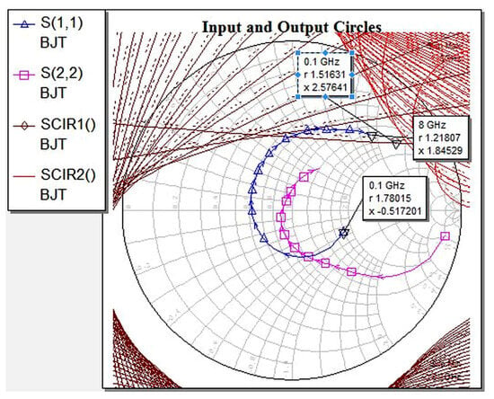
Figure 2.
Input and output stability circles of the selected BJT at 2 GHz.
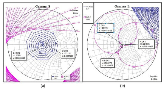
Figure 3.
(a) Selected source reflection coefficient (ΓS) and (b) selected load reflection coefficient (ΓL).
The selected active device is the NXP BFG425W transistor, biased at VCE = 2 V and IC = 25 mA. This device is well-suited for wideband LNA applications due to its high gain, low noise characteristics, and relatively low feedback capacitance [13]. The transistor is provided in a compact SOT-343R surface-mount package, which supports integration into planar RF front-end modules.
The complete circuit schematic is shown in Figure 4. Both the input and output matching networks employ open-ended microstrip stubs whose lengths and widths are optimized in AWR to realize the selected ΓS and ΓL.
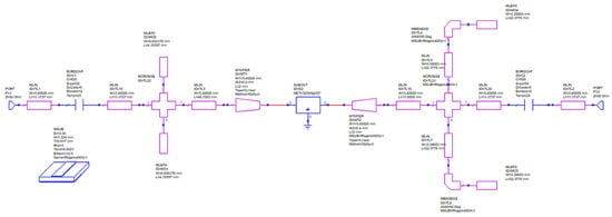
Figure 4.
Complete schematic of the proposed LNA.
After optimization, the simulated reflection coefficients S11 and S22 remain well below the oscillation threshold across the operating band, confirming effective matching and stable operation, as shown in Figure 5a,b.
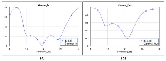
Figure 5.
(a) Circuit-level simulated input return loss (ΓIN) and (b) output return loss (ΓOUT) of the proposed LNA.
Figure 6 presents the circuit-level simulated input and output voltage standing-wave ratios (VSWR), which remain below 2 over the entire design bandwidth.
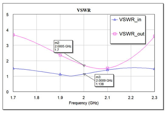
Figure 6.
Circuit-level simulated input and output VSWR of the proposed LNA.
The circuit-level simulated gain response, shown in Figure 7, exceeds 17 dB from 1.7 to 2.3 GHz, consistent with the transistor’s datasheet maximum gain of approximately 18 dB under ideal conditions.
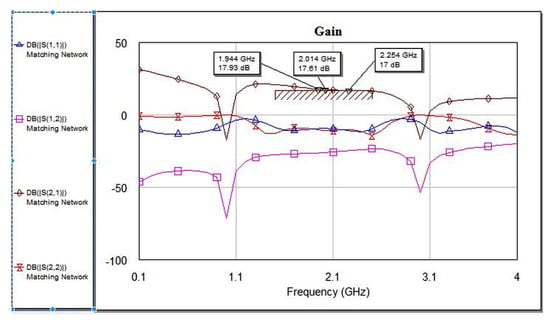
Figure 7.
Circuit-level simulated small-gain of the proposed LNA.
Following circuit-level optimization, the layout is exported as a DXF file and refined using full-wave EM simulation in Sonnet Software. DC blocking is implemented using 470-pF capacitors at the input and output ports. The bias network consists of cascaded low impedance and high-impedance quarter-wavelength transmission line sections, as illustrated in Figure 8.
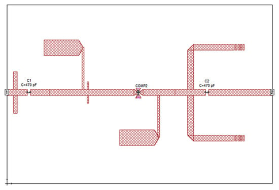
Figure 8.
EM layout of the proposed LNA.
This structure provides effective DC access while presenting a high impedance to RF signals, thereby preserving the wideband matching characteristics of the amplifier.
3. EM Simulation and Measurement Results
Initially, the proposed LNA was evaluated through circuit-level simulation in AWR Microwave Office to verify its stability, impedance matching, gain, and noise performance. Upon completion of circuit optimization, the physical layout was exported and then refined using full-wave electromagnetic simulation in Sonnet Software to accurately account for coupling effects, discontinuities, and substrate-related parasitics.
Sonnet Software was selected for electromagnetic simulation because it provides a well-established planar method-of-moments solver with open-boundary conditions that is particularly suitable for accurately modeling distributed microstrip structures and substrate-related parasitic effects on printed circuit boards. The EM-simulated S-parameters confirm stable wideband operation across the 1.7–2.3 GHz frequency range. At the circuit level, the simulated small-signal gain exceeds 17 dB across most of the operating band; when layout-dependent electromagnetic effects are included, the EM-simulated gain reaches a peak value of approximately 14.78 dB at the center frequency. The input and output reflection coefficients remain below −10 dB over the intended operating range, demonstrating effective wideband impedance matching. The simulated input and output VSWRs remain below 2, indicating good impedance stability and minimal distortion. These simulation results demonstrate that the selected reflection coefficients and distributed matching networks provide stable gain, low reflection, and predictable impedance behavior prior to fabrication. In the EM simulation stage, the complete passive matching networks, bias lines, and interconnects are modeled using Sonnet’s method-of-moments solver. Finite conductor thickness, dielectric loss, and metallization loss are included to capture the dominant PCB-related parasitic effects. Port definitions are applied at the SMA launch interfaces to account for realistic excitation conditions. This EM refinement step is used to validate the distributed matching networks and to bridge the gap between ideal circuit-level simulations and measured performance.
The LNA prototype is fabricated on a 60-mil Rogers RO4003C substrate, Rogers Corporation, Chandler, AZ, USA, using an LPKF ProtoMat S103 milling machine, LPKF Laser and Electronics SE, Garbstan, Germany. The fabricated design is shown in Figure 9. Experimental characterization is carried out using a vector network analyzer, spectrum analyzer, signal generator, and noise-figure analyzer (Keysight Technologies, Inc., Santa Rosa, CA, USA). For S-parameter measurements, the fabricated LNA is characterized using a calibrated vector network analyzer with coaxial SMA connections at the input and output ports following standard two-port calibration procedures. Noise-figure measurements are performed using a noise-figure analyzer with a calibrated noise source connected to the LNA input, while the output is terminated with a 50 Ω load under the nominal bias conditions. Linearity measurements are conducted using a two-tone setup in which closely spaced tones generated by signal sources are applied to the LNA input, and the output spectrum is observed using a spectrum analyzer. All measurements were carried out using the same bias conditions applied in the simulation. The measurement procedure follows standard two-port RF amplifier characterization and therefore does not require a dedicated setup diagram for reproducibility. Figure 10 compares the EM-simulated and measured S-parameters of the proposed LNA. At 2 GHz, the measured input return loss (S11) is −18.36 dB, while the simulated value is −23.92 dB. The measured output return loss (S22) is −7.89 dB, compared to −11.7 dB obtained from EM simulation. The measured small-signal gain is 13.84 ± 1 dB over the 1.75–2.25 GHz frequency range, whereas the EM-simulated gain is approximately 14.78 dB. The decrease in gain from circuit-level to EM simulation and measurement is mainly caused by conductor loss, dielectric loss, and connector transitions, which are not fully represented in ideal circuit-level models. The simulated and measured voltage standing-wave ratios (VSWR) are shown in Figure 11a,b. At the input port, the simulated VSWR is 1.136, while the measured value is 1.275, showing similar frequency-dependent behavior across the operating band. Although a small difference is observed, both results show similar frequency-dependent behavior across the operating band, indicating good agreement between simulation and measurement.
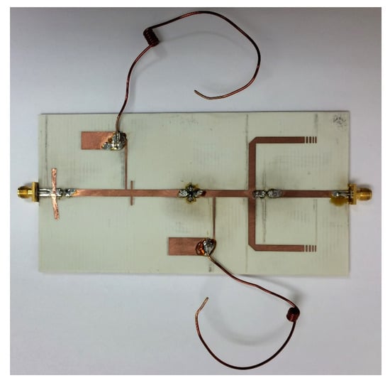
Figure 9.
Image of the fabricated prototype.
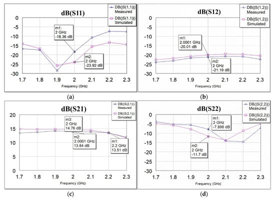
Figure 10.
Comparison of the simulated and measured S-parameters of the proposed LNA. (a) dB (S11), (b) dB (S12), (c) dB (S21), (d) dB (S22).
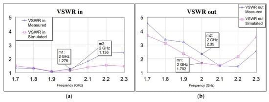
Figure 11.
Simulated and measured input and output VSWR. (a) VSWR in (b) VSWR out.
At the output port, the simulated VSWR is 1.702, while the measured value reaches approximately 2.35. This discrepancy is primarily due to fabrication tolerances, connector transitions, and layout-dependent parasitic effects that are difficult to fully capture in circuit- and EM-level simulations. Improved output matching could be achieved through tighter fabrication control or a second design iteration.
The measured noise figure of the LNA is shown in Figure 12. A minimum noise figure of 1.615 dB is achieved at 2 GHz, and the noise figure remains relatively flat from 1.75 to 2.2 GHz. According to the manufacturer’s datasheet, the typical noise figure of the NXP BFG425W transistor at 2 GHz under the same bias conditions of VCE = 2 V and IC = 25 mA exceeds 2 dB. It should be noted that datasheet noise figures are typically specified for a 50 Ω source impedance, whereas the proposed design employs impedance matching optimized for wideband operation and stability, which can result in a lower effective noise figure. Noise-figure results are therefore reported based on experimental measurements, and circuit-level noise-figure simulations are not included.
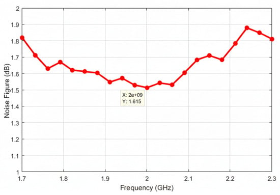
Figure 12.
Measured noise figure versus frequency.
The improved noise performance achieved in this work is attributed to the optimized distributed matching networks and the deliberate trade-off between noise figure, gain flatness, and output matching. This result shows that the distributed matching approach effectively controls the impedance seen by the transistor.
Linearity performance is evaluated using 1 dB gain compression and two-tone intermodulation measurements. The measured 1 dB gain compression point (P1dB) is shown in Figure 13 and is obtained at the center frequency of 2 GHz. The amplifier enters gain compression at an input power level of approximately 0.5 dBm. This behavior is consistent with the selected bias conditions and the moderate gain level targeted in the proposed design.
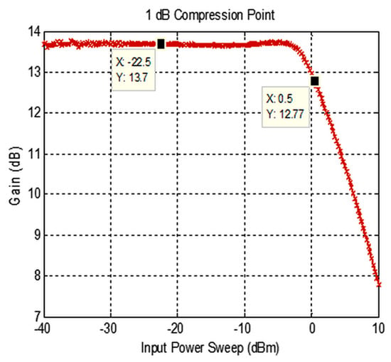
Figure 13.
Measured 1 dB compression point of the proposed LNA at 2 GHz.
To further evaluate nonlinear behavior, a two-tone intermodulation test is carried out using two equal-amplitude input tones applied around 2 GHz. The frequency spacing between the tones is kept small (on the order of 1 MHz) so that third-order intermodulation products appear close to the fundamental tones without overlapping them. The resulting output spectrum is measured using a spectrum analyzer, as shown in Figure 14.
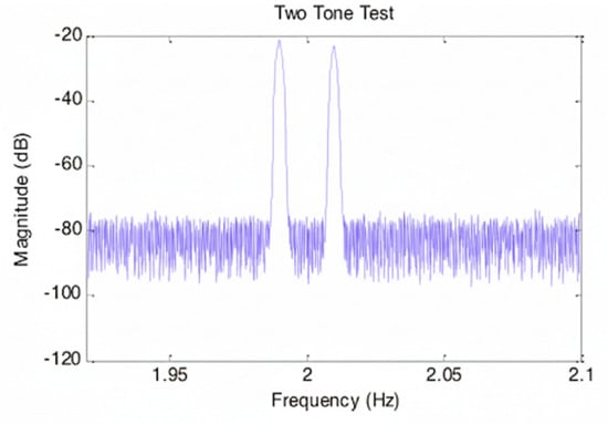
Figure 14.
Output spectrum of the two-tone test at low input power.
At low input power levels (below −30 dBm per tone), only the fundamental frequency components are observed at the output. As the input power is increased to approximately −18 dBm per tone, third-order intermodulation products become clearly visible, as shown in Figure 15. The emergence of these components indicates the onset of nonlinear operation and is consistent with the measured P1dB behavior. Given the intended role of the proposed amplifier as a low-noise, wideband front-end stage operating at moderate power levels, the two-tone measurement is used to verify the onset and trend of third-order distortion rather than to extract large-signal intercept points. The observed intermodulation behavior confirms that the proposed LNA exhibits acceptable linearity for sub-6-GHz receiver front-end applications, where low noise figure and stable wideband operation are typically prioritized over high large-signal linearity.
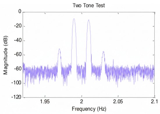
Figure 15.
Output spectrum of the two-tone intermodulation test showing third-order intermodulation.
4. Performance Comparison
A direct comparison of performance among low-noise amplifiers operating over extended bandwidths and implemented using different semiconductor technologies is inherently difficult, as these designs are often optimized under distinct constraints related to fabrication process, integration level, cost, and target application. Accordingly, the comparison presented in Table 1 is intended to position the proposed LNA within the broader background of reported wideband designs, rather than to rank performance across fundamentally different technologies. To this end, both discrete PCB-based LNAs and integrated implementations are included, with emphasis placed on practical sub-6-GHz receiver front-end realizations. As shown in Table 1, several wideband LNAs reported in the literature achieve high gain or low noise figure through the use of integrated CMOS or MMIC technologies. For example, PCB-based distributed matching designs are reported in [8,14,15], while GaAs pHEMT MMIC implementations in [16] demonstrate wideband operation with low noise figure over multi-gigahertz bandwidths, and SiGe BiCMOS and CMOS-based designs in [17] benefit from high integration density and compact module integration. Although these integrated approaches can provide high performance, they usually depend on specialized fabrication processes. This makes them less suitable for low-cost designs or for applications where quick tuning and modification are required.

Table 1.
Performance comparison of wideband LNAs using different technologies.
Discrete PCB-based LNAs remain a practical option for application-specific receiver front ends because they are easier to fabricate and modify. Some of these works focus on achieving high gain through multi-stage designs [8], while others are optimized for operation at a single or narrow frequency band [15]. In some cases, very low noise figures are reported, but the results are obtained mainly from simulations or under limited operating conditions [14]. In contrast, the performance of the proposed LNA is verified entirely through experimental measurements, providing a realistic evaluation of a practical PCB-based implementation.
Power consumption is an important factor in LNA design. However, a direct comparison is not included in Table 1 because several of the referenced works do not clearly report DC power consumption or use very different biasing conditions and fabrication technologies. For reference, the proposed LNA operates with a collector voltage of 2 V and a bias current of 25 mA, which corresponds to a DC power consumption of about 50 mW. This power level is typical for discrete PCB-based LNAs designed for moderate gain and low noise operation. Within this context, the proposed LNA provides a reasonable balance between noise figure, gain, and impedance stability over a 600 MHz bandwidth centered at 2 GHz. Compared with other discrete PCB-based LNAs, the design achieves comparable performance using a simple and fully distributed matching network. The emphasis of this work is on stable wideband behavior and practical implementation, rather than on circuit complexity or aggressive performance optimization.
Overall, the comparison shows that the proposed LNA is not intended to compete with integrated or MMIC designs in terms of absolute performance. Instead, it provides a practical alternative for sub-6-GHz receiver applications where simple implementation, fabrication tolerance, and predictable measured performance over a relatively wide bandwidth are more important.
5. Conclusions
This work described the design and measurement of a 2 GHz low-noise amplifier implemented on a printed circuit board using a discrete BJT and fully distributed microstrip matching networks. The main focus of the design was stable operation, repeatable impedance behavior, and ease of implementation using standard PCB fabrication rather than having complex circuitry. The amplifier was fabricated on a 60-mil Rogers RO4003C substrate and evaluated using circuit simulations, EM simulations, and experimental measurements. The measured results show a gain of about 13.84 ± 1 dB over the 1.75–2.25 GHz frequency range. The minimum noise figure is 1.615 dB at 2 GHz, and acceptable input and output matching are maintained across the frequency band. Stable operation is observed over the full operating range. Linearity measurements indicate a 1 dB gain compression point of approximately 0.5 dBm at 2 GHz, which is consistent with the selected bias conditions and the intended use in receiver front-end applications. These results show that fully distributed microstrip matching networks can be effectively used for discrete PCB-based LNAs covering several hundred megahertz of bandwidth. Although the proposed amplifier does not target the highest performance achievable with integrated or MMIC solutions, it provides a practical balance between noise figure, gain, stability, and fabrication tolerance. For sub-6-GHz receiver front ends where low cost, predictable measurements, and implementation robustness are important, the proposed design represents a reliable and reproducible solution.
Author Contributions
Conceptualization, M.O.K.; methodology, M.O.K.; software, M.O.K. and S.G.; validation, M.O.K. and S.G.; formal analysis, M.O.K. and S.G.; investigation, M.O.K. and S.G.; resources, M.O.K. and S.G.; data curation, M.O.K. and S.G.; writing—original draft preparation, M.O.K.; writing—review and editing, M.O.K. and S.G.; visualization, M.O.K. and S.G. All authors have read and agreed to the published version of the manuscript.
Funding
This research received no external funding.
Data Availability Statement
The data presented in this study are available from the corresponding author upon reasonable request.
Conflicts of Interest
The authors declare no conflicts of interest.
References
- Gonzalez, G. Microwave Transistor Amplifiers: Analysis and Design, 2nd ed.; Prentice Hall: Upper Saddle River, NJ, USA, 1997. [Google Scholar]
- Friis, H.T. Noise figures of radio receivers. Proc. IRE 1944, 32, 419–422. [Google Scholar] [CrossRef]
- Pozar, D.M. Microwave Engineering, 4th ed.; Wiley: Hoboken, NJ, USA, 2012. [Google Scholar]
- Oughton, E.; Geraci, G.; Polese, M.; Shah, V.; Bubley, D.; Blue, S. Reviewing wireless broadband technologies in the peak smartphone era: 6G versus Wi-Fi 7 and 8. Telecommun. Policy 2024, 48, 102766. [Google Scholar] [CrossRef]
- Elegaard, C.; Özen, M.; Westesson, E.; Mahmoud, A.; Torres, F.; Bint Reyaz, S. Efficient wideband mmW transceiver front end for 5G base stations in 22-nm FD-SOI CMOS. IEEE J. Solid-State Circuits 2023, 59, 321–336. [Google Scholar] [CrossRef]
- Lo, Y.T.; Kiang, J. Design of wideband LNAs using parallel-to-series resonant matching network between common-gate and common-source stages. IEEE Trans. Microw. Theory Techn. 2011, 59, 2285–2294. [Google Scholar] [CrossRef]
- Rangaiah, P.; Kumaraswamy, H.V. A 1-5 GHz hybrid MIC wideband LNA utilizing microstrip geometric structure variety for performance improvement. Trans. Netw. Commun. 2017, 5, 15. [Google Scholar] [CrossRef]
- Munir, A.; Taryana, Y.; Yunus, M.; Nusantara, H.; Effendi, M.R. Two-stage S-band LNA development using non-simultaneous conjugate match technique. J. ICT Res. Appl. 2019, 13, 213–220. [Google Scholar] [CrossRef]
- Rollett, J.M. Stability and power-gain invariants of linear twoports. IRE Trans. Circuit Theory 1962, 9, 29–32. [Google Scholar] [CrossRef]
- Cadence Design Systems. AWR Design Environment Platform. 2025. Available online: https://www.cadence.com/en_US/home/tools/system-analysis/rf-microwave-design/awr-design-environment-platform.html (accessed on 11 October 2025).
- Sonnet Software Inc. User’s Guide: The Analysis Engine (EM), version 18. 2025. Available online: https://www.sonnetsoftware.com/support/ (accessed on 11 October 2025).
- Rogers Corporation. RO4003C™ Laminates (Dk ≈ 3.55). Datasheet. 2025. Available online: https://www.rogerscorp.com/advanced-electronics-solutions/ro4000-series-laminates/ro4003c-laminates (accessed on 18 December 2025).
- NXP Semiconductors. BFG425W-NPN 25-GHz Wideband Transistor Data Sheet. 2025. Available online: https://www.nxp.com/docs/en/data-sheet/BFG425W.pdf (accessed on 11 October 2025).
- Belen, M.A.; Güneş, F. Surrogate-based design optimization of low-noise amplifier for ISM band. Sigma J. Eng. Nat. Sci. 2022, 40, 491–499. [Google Scholar] [CrossRef]
- Ouerghemmi, S.; Fakhfakh, A.; Derbel, F. A low-power 868 MHz BJT-based LNA with microstrip matching for wake-up receivers in IoT applications. Electronics 2025, 14, 2429. [Google Scholar] [CrossRef]
- Zhao, J.; Wang, F.; Yu, H.; Zhang, S.; Wang, K.; Liu, C.; Wan, J.; Liang, X.; Yan, Y. Analysis and design of a wideband low-noise amplifier with bias and parasitic parameters derived wide bandpass matching networks. Electronics 2022, 11, 633. [Google Scholar] [CrossRef]
- Tunç, A.; Ceylan, O.; Yağcı, H.B.; Paker, S. SiGe HBT low-noise amplifier module for sub-six 5G receivers. In Proceedings of the 27th Telecommunications Forum (TELFOR), Belgrade, Serbia, 26–27 November 2019; pp. 1–4. [Google Scholar] [CrossRef]
Disclaimer/Publisher’s Note: The statements, opinions and data contained in all publications are solely those of the individual author(s) and contributor(s) and not of MDPI and/or the editor(s). MDPI and/or the editor(s) disclaim responsibility for any injury to people or property resulting from any ideas, methods, instructions or products referred to in the content. |
© 2026 by the authors. Licensee MDPI, Basel, Switzerland. This article is an open access article distributed under the terms and conditions of the Creative Commons Attribution (CC BY) license.
