Abstract
This work presents a notch filter architecture based on a dual-output second-generation voltage conveyor, designed with a current-mode approach. The proposed topology employs a single frequency-selective LC branch and directly uses the two voltage outputs of the DOVCII to generate a notch response without additional active stages. Analytical expressions for the transfer function, notch frequency, and quality factor are derived, highlighting independent control of the passband gain and notch parameters. A sensitivity analysis demonstrates that the notch frequency depends exclusively on the LC product with half-order sensitivities, while the quality factor is predominantly controlled by a single resistor, resulting in predictable tuning and improved tolerance to passive component variations. Transistor-level analysis of the proposed filter was carried out using a standard AMS 0.35 μm CMOS process and has been validated through both circuit-level simulations and experimental measurements using a DOVCII implementation based on the AD844 current-feedback amplifier. Prototypes operating at 100 kHz and 50 Hz notch frequencies have been implemented, the latter employing a current-mode inductance simulator to avoid bulky passive inductors.
1. Introduction
Notch (band-stop) filters are widely used in analog signal-processing systems to suppress narrow-band interference while preserving the surrounding signal spectrum. Typical examples include the rejection of power-line components at 50/60 Hz in biomedical front-ends and the attenuation of undesired carriers or spurious tones in communication and sensor-conditioning circuits. In these applications, the filter is often required to provide a deep and accurately positioned notch, together with stable passband gain and predictable behavior under component tolerances.
In practical implementations, notch filtering is also relevant in audio electronics [1], sensor interfaces [2], and mixed-signal read-out circuits [3], where unwanted tonal components may limit dynamic range or degrade signal integrity. In such contexts, the filter architecture must simultaneously address selectivity, linearity, and robustness, often under low-voltage and low-power constraints. These requirements motivate the search for compact topologies with reduced component count and well-defined parameter control.
Conventional notch filters are commonly realized using voltage-mode operational amplifiers combined with passive RLC or active-RC networks [4,5]. While these solutions are well established, they may exhibit limited performance when implemented in integrated or low-voltage environments. In particular, deep notches often require precise component matching, multiple active stages, or large passive elements, leading to increased power consumption and reduced scalability. Furthermore, the gain–bandwidth trade-off and slew-rate limitations of voltage-mode amplifiers can become critical at higher frequencies.
Current-mode circuit techniques offer an alternative approach to filter synthesis [6,7,8,9]. By processing signals as currents rather than voltages, these architectures reduce the impact of parasitic capacitances, relax gain–bandwidth constraints, and enable simpler feedback and summation mechanisms [10]. As a result, current-mode filters can achieve wider bandwidth, improved linearity, and lower sensitivity to non-idealities, making them suitable for both low-frequency interference suppression and high-frequency signal conditioning [11,12].
Among current-mode active elements, current and voltage conveyor-based structures have gained significant attention due to their favorable internal characteristics and ease of use in filter synthesis [13]. In particular, the second-generation voltage conveyor (VCII) combines a low-impedance current input with a high-impedance internal terminal and low-impedance voltage output, effectively decoupling current and voltage processing. This dual-domain nature allows designers to exploit current summation and voltage buffering simultaneously, leading to flexible and efficient implementations of analog functions, including filters, sensor read-out circuits, and impedance simulators [14,15,16,17].
The availability of multi-output conveyor structures further extends the design flexibility. Dual-output current- or voltage-mode elements allow subtraction and differential signal processing to be implemented intrinsically, without additional active stages [18]. This feature is especially advantageous in notch filters, where the notch response is often obtained through the subtraction of frequency-selective signal paths.
In this work, a DOVCII-based notch filter is introduced, in which the notch behavior originates from the current balance at the low-impedance Y terminal. The input signal and the LC-dependent feedback signal are summed in the current domain, and the resulting current determines the voltage at the high-impedance X node through a resistive transimpedance. The two voltage outputs of the DOVCII provide equal-magnitude, opposite-polarity replicas of this voltage, enabling the realization of a biquadratic notch transfer function with a single frequency-selective branch and no additional active stages.
Unlike previously reported VCII-based notch filters, the proposed solution employs an explicit LC feedback branch and exploits the dual-output nature of the DOVCII to generate the notch responses.
Analytical expressions for the transfer function, notch frequency, and quality factor are derived, showing that the notch frequency depends exclusively on the LC product, while the quality factor is mainly controlled by a single resistor. This separation of roles simplifies the design procedure and improves robustness with respect to passive component tolerances. The proposed filter is validated through transistor-level simulations and experimental measurements, demonstrating its applicability to both high-frequency and low-frequency notch filtering.
The paper is organized as follows: Section 2 reviews the second-generation voltage conveyor and its main characteristics. Section 3 describes the realization of the proposed dual-output VCII. Section 4 presents the DOVCII-based notch filter architecture and its analytical characterization. Section 5 reports simulation and experimental results, followed by conclusions in Section 6.
2. Second-Generation Voltage Conveyor
The VCII can be regarded as the dual counterpart of the well-known second-generation current conveyor (CCII). In recent years, it has emerged as a valid alternative to both conventional voltage-mode circuits and CCII-based solutions [19,20,21,22,23]. Similar to the CCII, the VCII processes information using both current and voltage signals; however, it features separate voltage input and output terminals, which considerably simplifies voltage sensing and represents a key advantage over CCII-based implementations. Compared with traditional voltage-mode building blocks, the VCII offers several additional benefits, including independence between gain and bandwidth, enhanced slew rate, reduced noise, wider dynamic range, and a more straightforward circuit realization. Owing to the CCII–VCII duality, analytical methods originally developed for CCII-based circuits can be directly extended to VCII-based designs.
Figure 1 illustrates the symbolic representation of the VCII together with its equivalent circuit model. Under ideal conditions, the VCII behaves as a current follower between terminals Y and X, while simultaneously operating as a voltage buffer from terminal X to terminal Z.
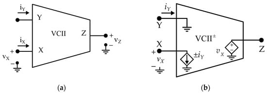
Figure 1.
Second-generation voltage conveyor: (a) symbol; (b) equivalent model.
It can be observed that the first stage of VCII has ideally zero input impedance seen from the Y terminal, and the X terminal impedance goes to infinity, whereas the Z terminal of VCII brings zero output impedance.
The ideal voltage–current relationships of a VCII are defined by the following matrix:
where and β are considered ideally unitary.
In this context, the sign of β identifies the polarity of the VCII, corresponding to the positive or negative configurations, referred to as VCII+ and VCII−, respectively.
A more realistic description of the VCII behavior, accounting for non-ideal effects, is provided by the following voltage–current relationship matrix:
where and denote the parasitic resistance and capacitance at the X terminal, and correspond to the parasitic resistance and inductance related to the Y terminal, and finally, and represent the parasitic resistance and inductance associated with the Z terminal, respectively. The VCII symbol, including internal parasitic terminal impedances, is also reported in Figure 2.
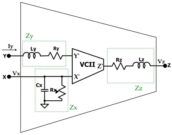
Figure 2.
VCII symbol with parasitic terminal impedances.
A possible internal architecture of a VCII is shown in Figure 3. The internal architecture consists of two main stages, namely a current buffering stage and a voltage buffering stage. The current injected at the Y terminal is conveyed to the X terminal with approximately unity gain through a current buffer implemented by transistors M1–M7. Voltage transfer between terminals X and Z is instead achieved using a flipped voltage follower (FVF) realized using transistors M9 and M10, which ensures a low output impedance at the Z terminal. A feedback network formed by transistors M1–M5 is responsible for establishing a low input impedance at the Y terminal. The simulated voltage and current gains, along with the terminal impedances and associated parasitic elements of the adopted VCII, are summarized in Table 1. The VCII has been designed and verified through simulations using a standard AMS 0.35 µm CMOS technology and operates with a ±1 V supply voltage; transistor dimensions are shown in Table 2.
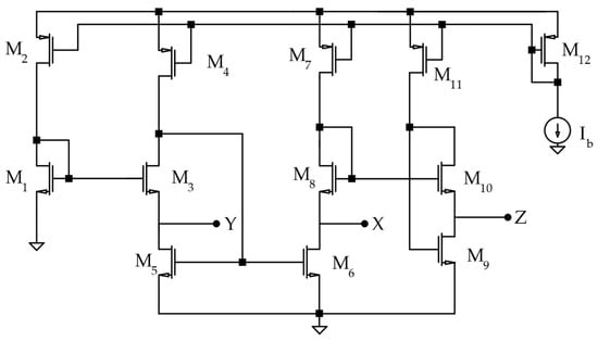
Figure 3.
CMOS implementation of the used VCII.

Table 1.
Simulated performance parameters of the VCII.
Table 2.
Transistor sizes.
3. Dual-Output VCII
The dual-output second-generation voltage conveyor (DOVCII) is the counterpart of the dual-output current conveyor (DOCCII) and an extension of the traditional VCII. Starting from the VCII, the DOVCII introduces two voltage output terminals, usually denoted as Z+ and Z−, which provide simultaneously non-inverting and inverting replicas of the voltage present at the high-impedance input terminal X. This property makes the DOVCII an attractive, active building block for the realization of wideband amplifiers and innovative filters where access to both polarities of the processed signal is beneficial.
From a functional point of view, the DOVCII inherits the port nature of the VCII. The Y terminal is a low-impedance current input node, the X terminal is a high-impedance node where the current injected at Y is conveyed, and the Z+ and Z− terminals are low-impedance voltage outputs. Ideally, the voltage at X is transferred to both Z+ and Z− with unit magnitude and opposite sign, while the current injected at Y is replicated at X with unit gain, inverting or non-inverting depending on the specific conveyor polarity.
The ideal port relations can be compactly written in matrix form. In the notations adopted in this work, the ideal DOVCII is described as follows:
The ideal DOVCII has α = 1 (with an opposite sign at Z+ and Z−) and β = ±1, whereas in practical implementations, finite gain, bandwidth limitations, and parasitic impedances cause both parameters to deviate from ideality, especially at high frequency.
A more realistic behavioral matrix, including the non-ideal parameters and parasitic terminal impedances, is therefore written as
In this work, the DOVCII is implemented firstly at the simulation level using the previously reported VCII and then fabricated at the board level employing the commercial device AD844 (Analog Devices, Inc., Norwood, MA, USA), a current-feedback operational amplifier, which, when suitably connected, can emulate both CCII and VCII behaviors thanks to its internal current-mode architecture and wide bandwidth.
The DOVCII structure is then obtained by combining two VCII blocks. The schematic reported in Figure 4 shows how two VCIIs are interconnected and how additional resistive elements are chosen to bias the device and to obtain the desired dual-output behavior, performing the correct I-V conversions. The values of the resistors have been tuned experimentally in LTspice to achieve a good compromise between gain accuracy, symmetric operation, and dynamic range on the two Z terminals.
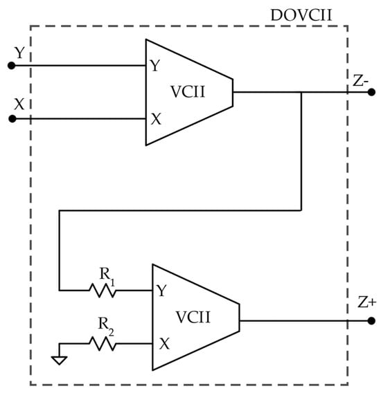
Figure 4.
Schematic of the proposed DOVCII, starting from two traditional VCIIs.
In the resulting configuration, terminal Y is implemented by the low-impedance input node of the first VCII, terminal X corresponds to its high-impedance current output node, while terminals Z+ and Z− are taken from the low-impedance voltage outputs of the two VCII stages, one configured in non-inverting and the other in inverting mode with respect to the voltage at X.
Figure 5 illustrates the typical time-domain behavior of the DOVCII, where the two output terminals Z+ and Z− provide correctly opposite-polarity replicas of the voltage present at terminal X, confirming the dual-output trend.
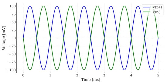
Figure 5.
Dual-output DOVCII operation.
4. DOVCII-Based Notch Filter
Figure 6 presents the circuit used as the basis of our proposed notch filter architecture. It consists of a DOVCII and a frequency-selective LC branch.
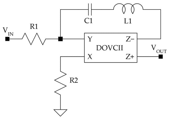
Figure 6.
The proposed DO-VCII-based notch filter.
Unlike most current-mode notch filters reported in the literature, which are typically derived from RC networks or CCII structures, the proposed architecture employs a single frequency-selective LC branch directly embedded in the feedback path of a dual-output voltage conveyor. The novelty of the proposed topology lies in the way the dual voltage outputs of the DOVCII are exploited. The positive output Z+ is directly used as the filter output, whereas the negative output Z− drives the LC feedback branch connected to the same low-impedance summing node Y. This intrinsic polarity inversion eliminates the need for additional subtraction or differential amplifier stages.
In this configuration, the input signal is applied to the low-impedance Y terminal through the resistor R1, while the high-impedance X terminal is connected to ground through the resistor R2 to perform an I-V conversion. Since the Y terminal exhibits a very low input impedance, the voltage VIN applied through R1 mainly sets a current flowing into Y. The dual-output nature of the DOVCII is then exploited by feeding the negative output Z− back to the input node Y through a frequency-selective LC network.
DOVCII enforces an almost ideal current transfer between Y and X, so that IY ≈ IX, while reproducing the voltage at terminal X at its two outputs, Z+ and Z− terminals with opposite polarity.
The positive output Z+ is used directly as the filter output, while the negative output Z− drives the series L–C network connected back to the summing node Y. The voltage at Z− thus generates a feedback current which is injected into the same low-impedance node Y that already receives the input current through R1.
The total current at the Y terminal is therefore the sum of the input and feedback contributions. Through the relation and the connection of X to the output via R2, this current balance determines the terminal voltage VX, hence the output voltage, as a frequency-dependent function of the input voltage.
Since the output voltage is simply VOUT = VZ+ ≈ VX, the overall transfer function H(s) takes the biquadratic notch form for an ideal VCII:
where the ratio R1/R2 sets the passband gain and the L–C network defines the notch frequency as follows:
To assess the robustness of the proposed notch filter with respect to component tolerances, a sensitivity analysis of the notch frequency f0 and quality factor Q is carried out.
Accordingly, the quality factor is given by
By considering a non-ideal VCII characterized by parasitic terminal impedances (Figure 2) and non-unitary α and β parameters, the resulting transfer function of the proposed filter can be derived from (5) as follows:
Adding the parasitic impedances at the X and Z terminals, where ZX and ZZ have been considered purely resistive for the chosen working frequencies, and neglecting ZY, the resulting relation becomes
The sensitivity of a filter parameter p (f0, Q) with respect to one of the passive elements x (R, C, L) is defined as follows:
Since the notch frequency depends only on the product LC, its sensitivity with respect to the circuit parameters are
Therefore, a relative variation of ±1% in either L or C results in a ±0.5% shift in the notch frequency, while f0 is ideally insensitive to the resistor R2.
With respect to the quality factor, the corresponding sensitivities are
Therefore, Q exhibits a unitary sensitivity to R1, meaning that a +1% variation in R2 produces a −1% variation in Q. Conversely, variations in L and C affect the quality factor with half-order sensitivity.
In addition to passive component tolerances, the performance of the proposed notch filter is affected by non-idealities of the active building block. In particular, finite values and mismatches of the voltage and current gains (α ≠ β), limited bandwidth, and asymmetry between the output impedances of the Z+ and Z− terminals may influence the depth and symmetry of the notch response.
From (8), it can be observed that deviations of αβ from unity primarily affect the damping term of the denominator, effectively modifying the apparent quality factor. As a result, active gain errors do not shift the notch frequency, which remains determined by the LC product, but they reduce the achievable notch depth and may minimally change the notch sharpness.
The effect of the load connected to the filter output can be analyzed by considering the low output impedance of the Z+ terminal of the DOVCII. In the proposed architecture, the load is not directly involved in the frequency-selective mechanism that determines the notch frequency and quality factor.
For resistive loads significantly higher than the intrinsic output resistance of the Z+ terminal, the frequency response remains essentially unchanged. In particular, the notch frequency, which is set by the LC product, is unaffected, while only minor variations in passband gain may occur due to finite output impedance effects. Under these conditions, the notch depth and selectivity are preserved.
When low-resistance loads are applied, comparable to the output impedance of the DOVCII, the increased current demand may introduce additional damping and slightly reduce the achievable notch depth. In the time domain, this may result in a modest attenuation of the output amplitude and, in extreme cases, in waveform distortion due to the large-signal limitations of the active block. However, the overall notch behavior and frequency accuracy remain primarily determined by the feedback network.
5. Simulations and Results
This section presents the experimental validation of the proposed DOVCII-based notch filter. Before performing laboratory measurements, extensive LTspice simulations were carried out using two of the previously validated CMOS VCII to make the DOVCII, ensuring accurate prediction of the expected notch response. Two operating conditions were investigated: a notch centered at 100 kHz, and another filter designed to reject the component at 50 Hz frequency, implemented with a physical inductor and with a floating-inductance simulator [24] to overcome practical limitations, respectively. All measurements were carried out using the AD844 device configured as a DOVCII, as detailed previously.
To validate the analytical transfer function, the first prototype targets a notch frequency of 100 kHz using the component set R1 = R2 = 1 kΩ, C = 500 pF, and L = 5 mH.
Simulation at the transistor level confirms the expected deep attenuation around 100 kHz, as illustrated by the Bode magnitude plot in Figure 7. The notch depth is pronounced, and the transition around the rejected band is sharp, demonstrating the theoretical selectivity predicted by the transfer function.
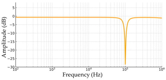
Figure 7.
Simulated notch operation at 100 kHz.
To verify the independent tuning of the quality factor predicted by the analytical model, resistance R2 was varied while keeping the LC product constant. Figure 8 shows the resulting frequency responses for different values of R2. As expected, modifying the resistance affects the notch bandwidth and selectivity, whereas the notch frequency remains fixed at 100 kHz. This behavior confirms the analytical expressions derived in Section 4 and validates the independent control of Q and f0.
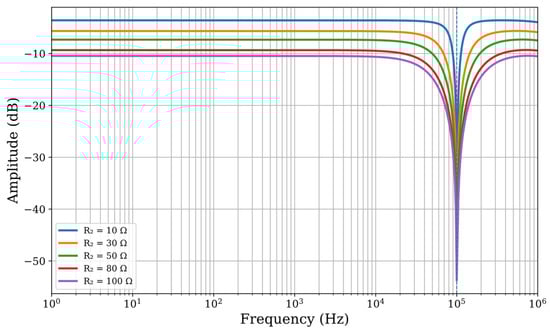
Figure 8.
Magnitude response of the proposed DOVCII-based notch filter for different values of R2.
To experimentally validate the transistor-level simulated response, a prototype of the designed notch filter was assembled on a breadboard and tested under the same operating conditions used in the LTspice simulations. The measurement setup shown in Figure 9 consisted of a KEYSIGHT 33600A Series waveform generator (Keysight Technologies, Santa Rosa, CA, USA) used to provide the input signal, while the output signals were captured using a KEYSIGHT MSOX3054T mixed-signal oscilloscope (Keysight Technologies, Santa Rosa, CA, USA) (500 MHz, 5 GSa/s). The circuit was powered by a KEYSIGHT E36313A precision DC supply (Keysight Technologies, Santa Rosa, CA, USA), ensuring stable and low-noise operating conditions during the tests.
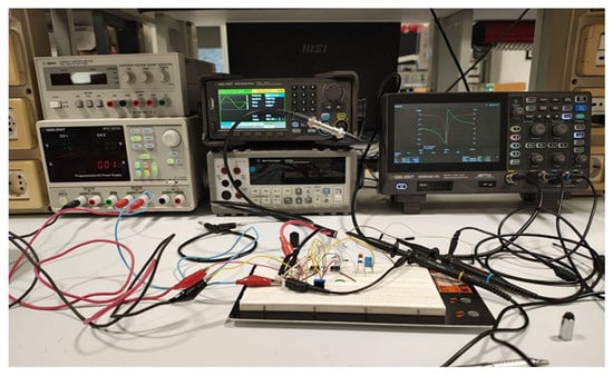
Figure 9.
Measurement setup.
The resulting output waveform, reported in Figure 10, closely matches the predicted behavior: the signal amplitude at the filter output is almost completely suppressed, demonstrating the correct formation of the attenuation notch. The time-domain response, shown in Figure 11, exhibits a stable cancellation with no observable distortions or unexpected transient effects, confirming the reliability of the DOVCII-based architecture under real hardware operation.
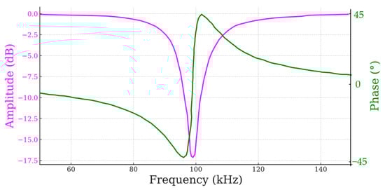
Figure 10.
Measured frequency performance of the proposed filter designed for 100 kHz operation.
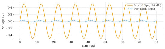
Figure 11.
Measured time-domain performance of the proposed filter designed for 100 kHz operation.
A second validation was conducted to assess the performance of the proposed architecture at low frequencies, specifically targeting a notch at 50 Hz, using the component set R1 = R2 = 1 kΩ, C = 500 nF, and L = 20 H. Achieving such a low resonant frequency using the classical RLC feedback structure would require an inductance on the order of several hundred millihenries or higher, as in this case. Besides being physically bulky, real inductors of this magnitude introduce significant series resistance and parasitic effects, degrading the depth and accuracy of the notch. For these reasons, the design was reformulated to preserve a fully current-mode structure by replacing the physical inductor with a VCII-based floating inductance simulator [24].
The inductance simulator, implemented using the same AD844 devices employed for the DOVCII realization, provides an equivalent impedance of the form Z(s) = sLeq, with Leq = R1R2C. This allows the desired inductive behavior to be synthesized using only resistors and capacitors, while maintaining high linearity and bandwidth consistency within the current-mode paradigm.
The simulated frequency response of the resulting 50 Hz notch filter is shown in Figure 12, confirming a well-defined attenuation notch centered at the designed frequency and a passband gain consistent with the chosen resistor ratio.
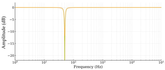
Figure 12.
Simulated notch operation at 50 Hz.
To experimentally validate the simulation results, the same configuration was implemented on a breadboard and measured using the laboratory setup described earlier. The measured response, reported in Figure 13, closely matches the simulated one: a clear notch appears at 50 Hz, and the surrounding passband exhibits the expected gain and linearity. The consistency between simulation and hardware measurements confirms the effectiveness of the VCII-based inductance simulator and highlights the suitability of the proposed DOVCII structure for low-frequency selective filtering without resorting to large passive inductors.
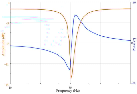
Figure 13.
Measured frequency performance of the proposed filter designed for 50 Hz operation.
The time-domain response is shown in Figure 14, where the 50 Hz sinusoidal input is severely suppressed at the filter output.
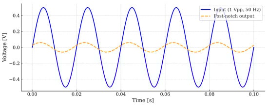
Figure 14.
Measured time-domain performance of the proposed filter designed for 50 Hz operation.
Linearity of the proposed notch filter was evaluated through total harmonic distortion (THD) simulations using LTspice harmonic analysis. To assess signal fidelity under normal operating conditions, THD was computed at the filter output by applying sinusoidal inputs in the passband region, well separated from the notch frequency. All reported input amplitudes refer to peak values, and harmonic analysis was performed on steady-state waveforms after transient settling.
Considering the filter design centered at 50 Hz, THD was evaluated using passband sinusoidal inputs both below and above the notch frequency. In particular, a 10 Hz input was used to characterize the lower passband region relevant to biomedical signal acquisition, while a 100 Hz input was used to assess linearity in the upper passband. At 10 Hz, THD remained below 0.4% for input amplitudes up to 20 mV, with measured values of 0.28%, 0.30%, and 0.36% for 5 mV, 10 mV, and 20 mV inputs, respectively, and increased to approximately 1.31% for a 100 mV input. Comparable behavior was observed at 100 Hz, confirming that distortion remains limited across the passband and that the observed increase at higher amplitudes is associated with large-signal operation of the active elements.
A similar analysis was carried out for the filter design centered on a 100 kHz notch. THD was computed by applying passband sinusoidal inputs at 1 kHz and 10 kHz. For a 10 mV input amplitude, THD remained as low as 0.05% at both test frequencies, whereas for a 100 mV input amplitude, THD increased to approximately 2.0% at 1 kHz and 1.6% at 10 kHz. These results are consistent with increased signal swing and bandwidth-related non-idealities of the active block at higher frequencies. The increase in distortion observed at higher input amplitudes is mainly due to the large-signal behavior of the active elements rather than to the filter topology itself.
Table 3 reports a comparison between the proposed DOVCII-based notch filter and representative state-of-the-art notch filter implementations, focusing on architectural and implementation aspects. The comparison includes both voltage-mode and current-mode solutions, covering different active building blocks, tuning strategies, and implementation technologies.
Table 3.
Literature comparison of notch filters.
The considered metrics focus on architectural and implementation aspects rather than absolute performance figures, which are often strongly dependent on the target application and technology. This allows a fair assessment of structural complexity, integration suitability, and signal-mode operation.
Previously reported solutions predominantly rely on OTA-based or CCII-based architectures, often requiring a relatively high number of passive components or multiple active blocks to achieve tunable notch characteristics. In contrast, the proposed approach exploits the dual-output nature of the DOVCII to realize the notch function with a reduced component count and without multiple stages. Moreover, the use of an active inductance enables low-frequency notch operation while preserving a fully current-mode signal processing paradigm.
6. Conclusions
In this work, a compact and versatile notch filter architecture based on a dual-output second-generation voltage conveyor has been presented and experimentally validated. The proposed solution exploits the intrinsic current-mode nature of the DOVCII and its dual, opposite-polarity voltage outputs to synthesize a biquadratic notch response using a minimal number of passive components and without the need for additional differential or subtraction stages. Analytical expressions for the transfer function, notch frequency, and quality factor have been derived, showing a clear separation of roles among circuit parameters.
In particular, the notch frequency is determined exclusively by the product of the reactive elements, while the quality factor is mainly controlled by a single resistor, resulting in low sensitivity to passive component tolerances and simplified tuning. This characteristic represents a significant advantage over traditional voltage-mode notch filters, especially in applications requiring predictable behavior and robustness.
The proposed topology has been thoroughly verified through transistor-level simulations and experimental measurements using an AD844-based DOVCII implementation. Two representative operating conditions have been investigated. The first prototype, operating at 100 kHz, demonstrates the suitability of the architecture for high-frequency applications, showing excellent agreement between theoretical predictions, simulations, and laboratory results. A second prototype targeting low-frequency operation at 50 Hz has been realized by replacing the physical inductor with a VCII-based floating inductance simulator. This approach preserves a fully current-mode structure while avoiding bulky and lossy passive inductors, achieving accurate notch placement and deep attenuation in both frequency- and time-domain measurements.
Beyond the presented validation, the proposed DOVCII-based notch filter is particularly relevant for practical applications requiring selective interference suppression. A notable example is the rejection of power-line interference at 50 Hz, which is a critical requirement in biomedical signal acquisition systems such as electrocardiography (ECG), electroencephalography (EEG), and electromyography (EMG). In these contexts, narrowband low-frequency noise can significantly compromise signal integrity and diagnostic reliability. The ability to realize an accurate and deep 50 Hz notch using a compact, fully current-mode architecture makes the proposed solution especially attractive for low-power and potentially integrated biomedical front-ends. At the same time, the demonstrated high-frequency operation highlights the versatility of the architecture for interference mitigation in sensor conditioning circuits, audio electronics, and mixed-signal systems, where unwanted tonal components must be selectively suppressed without affecting the surrounding signal spectrum.
Overall, the obtained results confirm that the DOVCII constitutes an effective and flexible active building block for the realization of notch filters over a wide frequency range. The proposed architecture combines compactness, high linearity, and design simplicity, making it well-suited for applications such as interference suppression in biomedical instrumentation, sensor conditioning, and mixed-signal front-ends.
Author Contributions
Conceptualization, R.O. and T.C.; methodology, T.C.; software, R.O. and T.C.; validation, R.O., G.B. and G.F.; formal analysis, G.F.; investigation, G.B. and G.F.; resources, V.S.; data curation, R.O.; writing—original draft preparation, R.O. and G.F.; writing—review and editing, G.B., V.S. and G.F.; visualization, R.O. and G.B.; supervision, G.B. and G.F.; project administration, V.S. and G.F.; funding acquisition, V.S. All authors have read and agreed to the published version of the manuscript.
Funding
This research received no external funding.
Data Availability Statement
The original contributions presented in this study are included in the article. Further inquiries can be directed to the corresponding author.
Conflicts of Interest
The authors declare no conflicts of interest.
References
- Wu, W.; Xiao, Y.; Lin, J.; Ma, L.; Khorasani, K. An efficient filter bank structure for adaptive notch filtering and applications. IEEE/ACM Trans. Audio Speech Lang. Process. 2021, 29, 3226–3241. [Google Scholar] [CrossRef]
- Bohorquez, J.L.; Yip, M.; Chandrakasan, A.P.; Dawson, J.L. A biomedical sensor interface with a sinc filter and interference cancellation. IEEE J. Solid-State Circuits 2011, 46, 746–756. [Google Scholar] [CrossRef]
- Yip, M.; Bohorquez, J.L.; Chandrakasan, A.P. A 0.6-V 2.9-µW mixed-signal front-end for ECG monitoring. In Proceedings of the 2012 Symposium on VLSI Circuits (VLSIC), Honolulu, HI, USA, 13–15 June 2012; pp. 66–67. [Google Scholar] [CrossRef]
- Denisenko, D.; Prokopenko, N. Active notch RC-filters of the fourth order with an adjustable delay band and uneven amplitude–frequency response. J. Commun. Technol. Electron. 2023, 68, 192–198. [Google Scholar] [CrossRef]
- Soliman, A. Active RC high selectivity notch filter. Int. J. Electron. 1974, 37, 565–567. [Google Scholar] [CrossRef]
- Yucel, F.; Yuce, E. CCII based more tunable voltage-mode all-pass filters and their quadrature oscillator applications. AEU Int. J. Electron. Commun. 2014, 68, 1–9. [Google Scholar] [CrossRef]
- Olivieri, R.; Di Lizio, G.A.; Barile, G.; Stornelli, V.; Ferri, G.; Minaei, S. Conveyor-based single-input triple-output second-order LP/BP and cascaded first-order HP filters. Electronics 2025, 14, 3514. [Google Scholar] [CrossRef]
- Jaikla, W.; Sangyaem, S.; Supavarasuwat, P.; Khateb, F.; Minaei, S.; Kulej, T.; Suwanjan, P. Reconfigurable voltage-mode first-order multifunction filter employing second-generation voltage conveyor (VCII) with complete standard functions and electronically controllable modification. IEEE Access 2023, 11, 56152–56169. [Google Scholar] [CrossRef]
- Yuce, E.; Safari, L.; Minaei, S.; Ferri, G.; Stornelli, V. New mixed-mode second-generation voltage conveyor based first-order all-pass filter. IET Circuits Devices Syst. 2020, 14, 901–907. [Google Scholar] [CrossRef]
- Safari, L.; Barile, G.; Ferri, G.; Stornelli, V. Traditional op-amp and new VCII: A comparison on analog circuits applications. AEU Int. J. Electron. Commun. 2019, 110, 152845. [Google Scholar] [CrossRef]
- Ahmadi, S.; Mahmoudi, A.; Maddipatla, D.; Bazuin, B.J.; Azhari, S.J.; Atashbar, M.Z. A current mode instrumentation amplifier with high common-mode rejection ratio designed using a novel fully differential second-generation current conveyor. SN Appl. Sci. 2023, 5, 34. [Google Scholar] [CrossRef]
- Mathur, C.; Pandey, R. High-performance second-generation current conveyor and its applications. Wirel. Pers. Commun. 2024, 139, 1863–1880. [Google Scholar] [CrossRef]
- Smith, K.C.; Sedra, A. The Current Conveyor—A New Circuit Building Block. Proc. IEEE 1968, 56, 1368–1369. [Google Scholar] [CrossRef]
- Al-Shahrani, S.M.; Al-Absi, M.A. Efficient inverse filters based on second-generation voltage conveyor (VCII). Arab. J. Sci. Eng. 2022, 47, 2685–2690. [Google Scholar] [CrossRef]
- Olivieri, R.; Esposito, P.; Fonte, M.; Barile, G.; Zompanti, A.; Ferri, G.; Stornelli, V. A current mode interface for dendrometry through an additively manufactured sensor. In Proceedings of the IEEE Sensors Applications Symposium (SAS), Newcastle, UK, 8–10 July 2025; pp. 1–6. [Google Scholar] [CrossRef]
- Shrivastava, M.; Bhaskar, D.R.; Kumar, P. VCII-based immittance simulators: Generalized parallel configurations. Int. J. Circuit Theory Appl. 2024, 53, 3754–3766. [Google Scholar] [CrossRef]
- Faseehuddin, M.; Shireen, S.; Herencsar, N.; Tangsrirat, W. Novel FDNR, FDNC and lossy inductor simulators employing second generation voltage conveyor (VCII). Int. J. Numer. Model. 2023, 36, e3100. [Google Scholar] [CrossRef]
- Wang, C.; Lin, H. Multifunction current differencing cascaded transconductance amplifier (MCDCTA) and its application to current-mode multiphase sinusoidal oscillator. J. Electr. Eng. 2015, 66, 241–249. [Google Scholar] [CrossRef]
- Yucehan, T.; Yuce, E. CCII-based voltage-mode and current-mode high-order filters with gains and grounded passive elements only. AEU Int. J. Electron. Commun. 2022, 155, 154346. [Google Scholar] [CrossRef]
- Guerrero, F.N.; Catacora, V.A.; Grasso, A.D.; Palumbo, G. Multi-electrode EMG spatial-filter implementation based on current conveyors. Electronics 2024, 13, 1735. [Google Scholar] [CrossRef]
- Djurić, R.; Popović-Božović, J. A CMOS rail-to-rail class AB second-generation voltage conveyor and its application in a relaxation oscillator. Electronics 2024, 13, 3511. [Google Scholar] [CrossRef]
- Theppota, B.; Jaikla, W.; Saksiri, W.; Siripruchyanun, M. VCII-based transimpedance-mode all-pass filter using single grounded capacitor. In Proceedings of the ECTI-CON, Khon Kaen, Thailand, 27–30 May 2024; pp. 1–6. [Google Scholar] [CrossRef]
- Ozer, E.; Kacar, F. Current-mode PID controller using second-generation voltage conveyor (VCII). J. Circuits Syst. Comput. 2022, 31, 2250295. [Google Scholar] [CrossRef]
- Verma, P.; Gupta, Y.; Tanwar, D.; Gupta, M.; Gautam, S.; Bansal, U. Second generation voltage conveyor based floating inductor and its applications. In Proceedings of the 2nd International Conference on Device Intelligence, Computing and Communication Technologies (DICCT), Dehradun, India, 15–16 March 2024; pp. 508–513. [Google Scholar] [CrossRef]
- Kumngern, M.; Khateb, F.; Kulej, T.; Arbet, D.; Akbari, M. Fully differential fifth-order dual-notch low-pass filter for portable EEG system. AEU Int. J. Electron. Commun. 2022, 146, 154122. [Google Scholar] [CrossRef]
- Mohan, J.; Maheshwari, S. Generalized current-mode configuration with low input and high output impedance. IU-J. Electr. Electron. Eng. 2016, 16, 1971–1979. [Google Scholar]
- Paul, S.K.; Choubey, C.K.; Tiwari, G. Low power analog comb filter for biomedical applications. Analog. Integr. Circuits Signal Process. 2018, 97, 371–386. [Google Scholar] [CrossRef]
- Sharma, S.; Rajput, S.S.; Pal, K.; Mangotra, L.K.; Jamuar, S.S. Low-voltage CCII based all-pass/notch filter. Indian J. Pure Appl. Phys. 2006, 44, 871–874. [Google Scholar]
- Ansari, M.S.; Sinha, R.; Khot, S. Ultra-low power 50/60 Hz notch filter for biomedical signal acquisition using 32 nm ±0.15 V bulk-driven subthreshold CMOS OTAs. In Proceedings of the 4th International Conference on Electrical and Electronic Engineering (ICEEE) 2017, Ankara, Turkey, 8–10 April 2017; IEEE: Piscataway, NJ, USA, 2017; pp. 309–313. [Google Scholar]
- Horng, J.-W. Three inputs and one output voltage-mode universal biquadratic filter using one CCII and one CCIII. J. Integr. Circuits Syst. 2023, 18, 1–4. [Google Scholar] [CrossRef]
Disclaimer/Publisher’s Note: The statements, opinions and data contained in all publications are solely those of the individual author(s) and contributor(s) and not of MDPI and/or the editor(s). MDPI and/or the editor(s) disclaim responsibility for any injury to people or property resulting from any ideas, methods, instructions or products referred to in the content. |
© 2026 by the authors. Licensee MDPI, Basel, Switzerland. This article is an open access article distributed under the terms and conditions of the Creative Commons Attribution (CC BY) license.