
A 48 nW, Universal, Multi-Mode Gm-C Filter with a Frequency Range Tunability


Abstract
1. Introduction
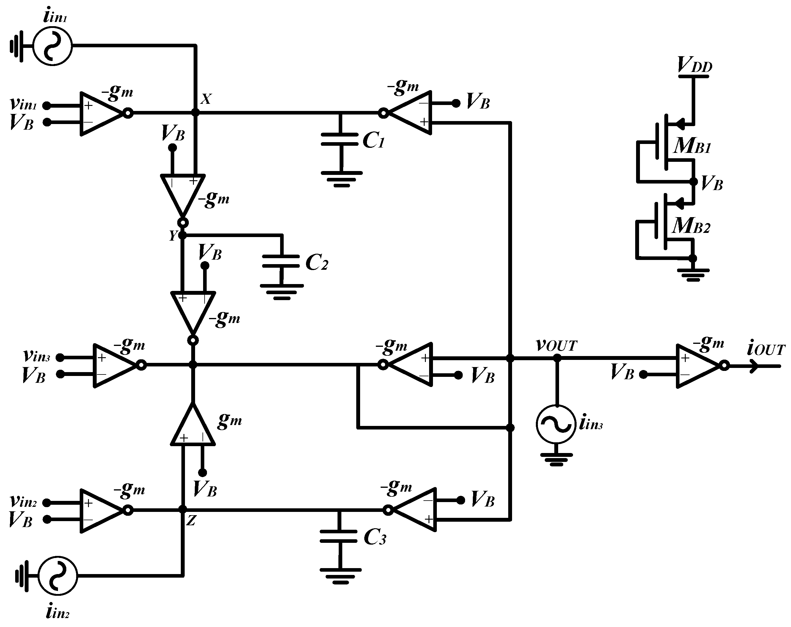
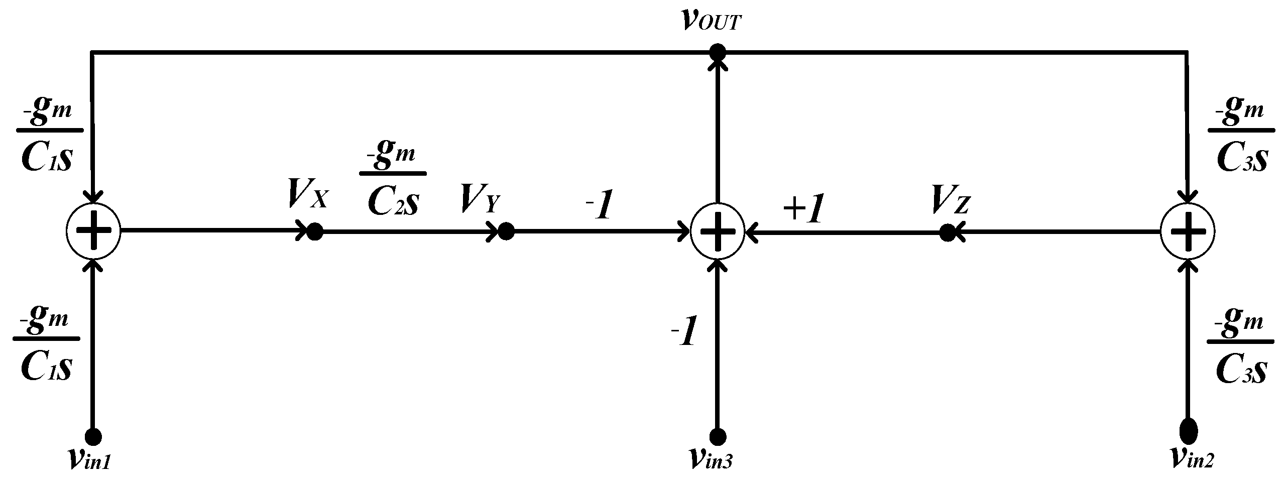
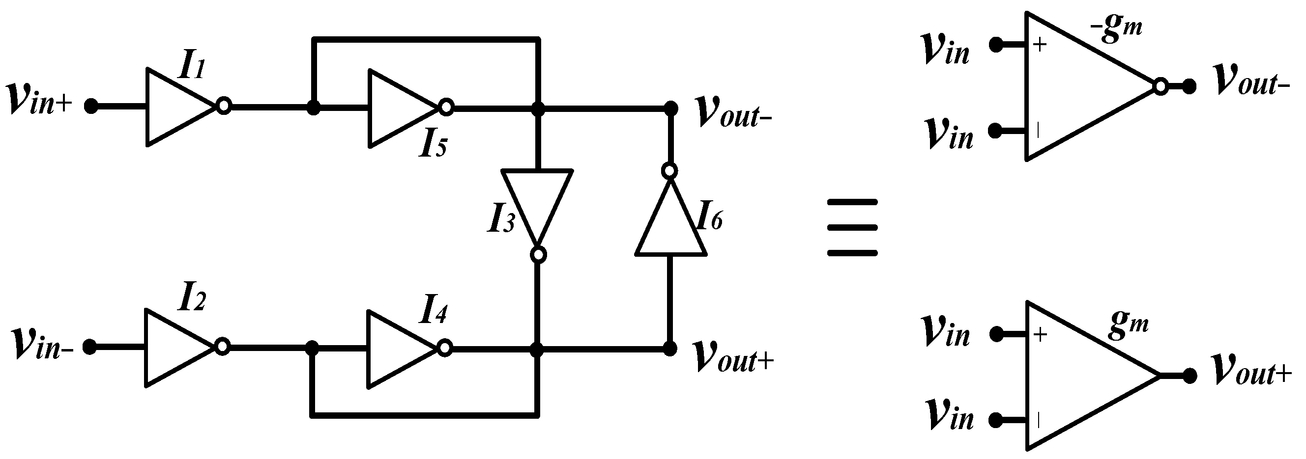
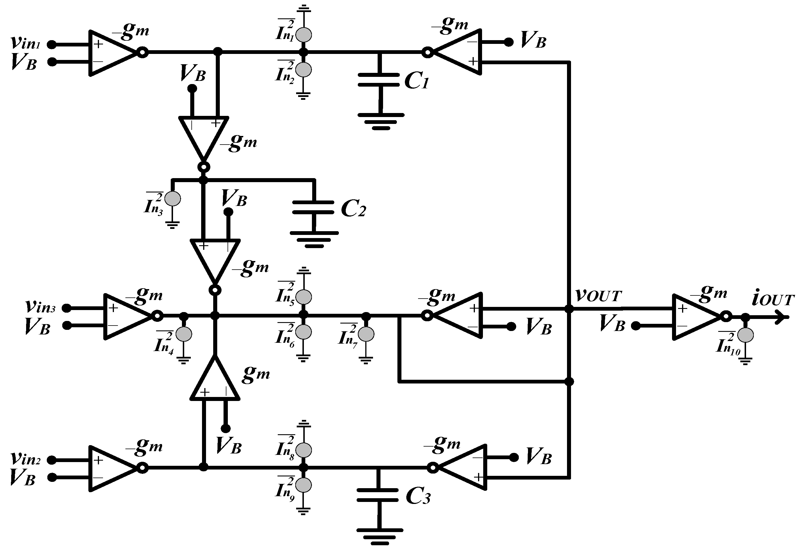
2. The Proposed Filter Design
2.1. Current and Trans-Resistance Modes
2.2. Voltage and Transconductance Modes
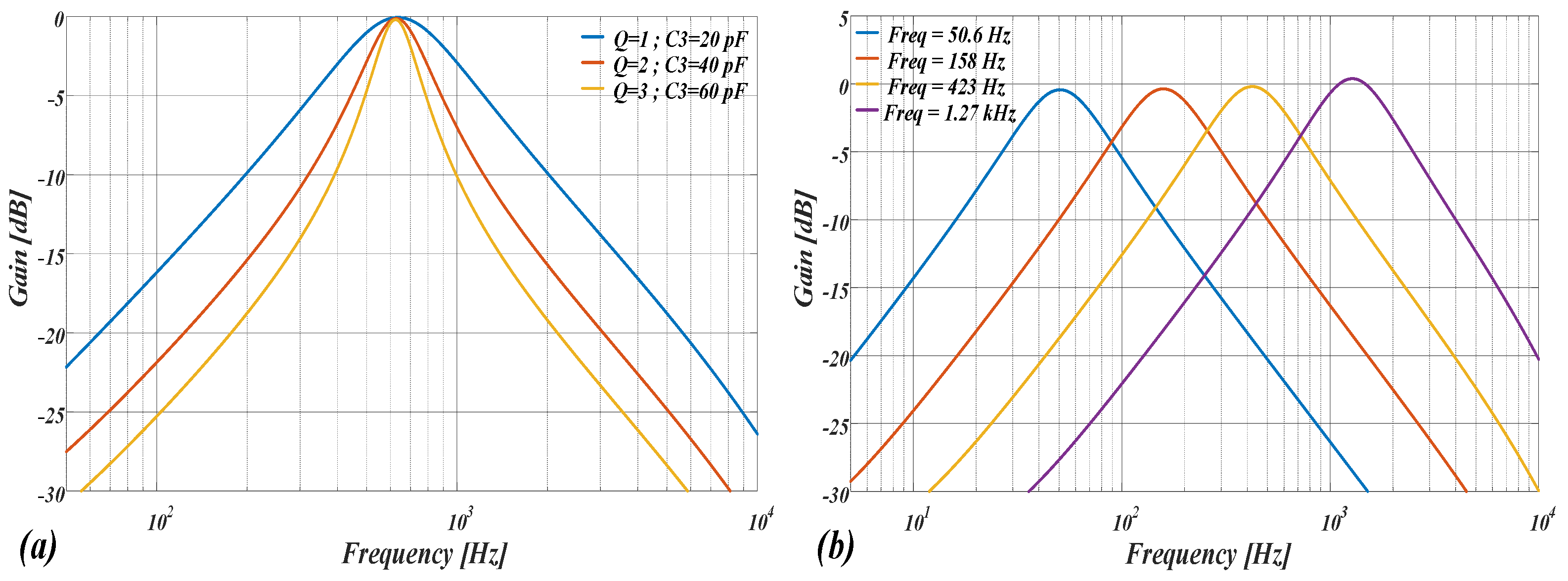
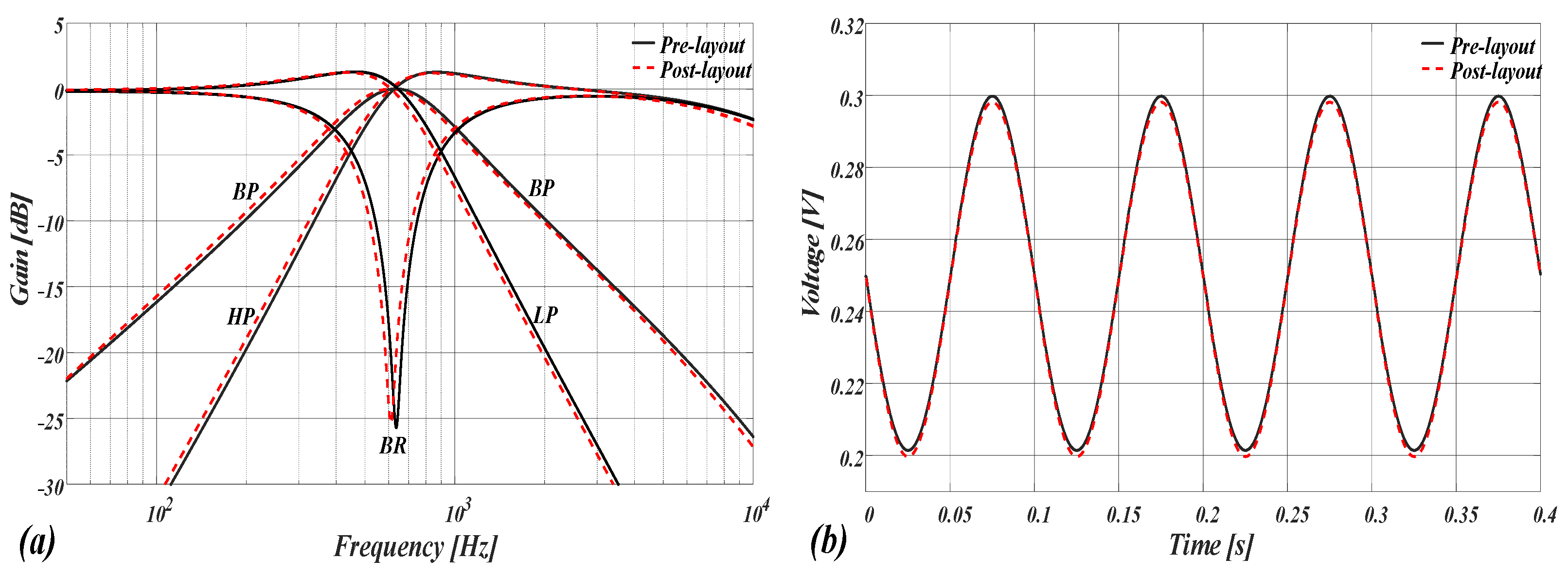
3. Simulation Results
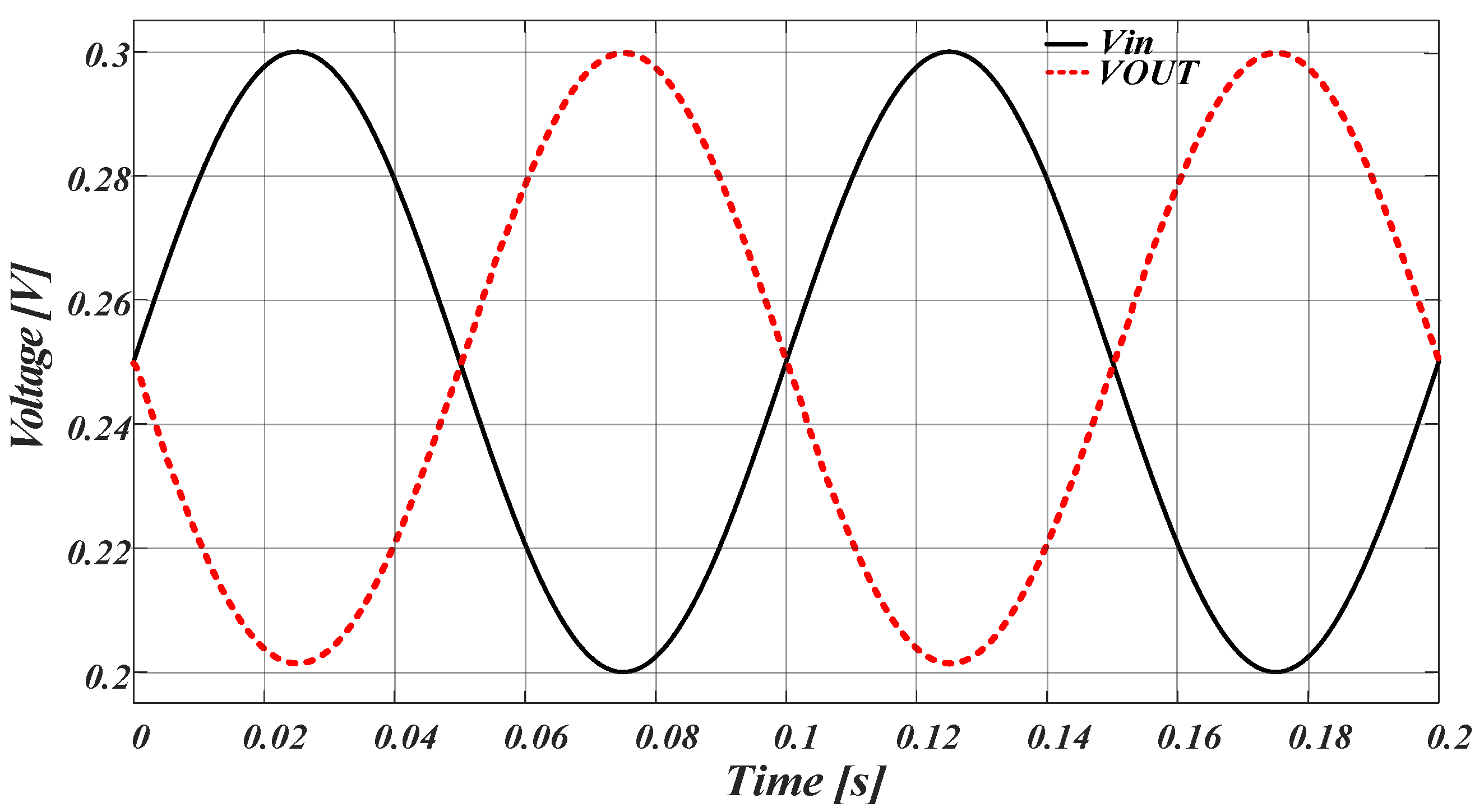
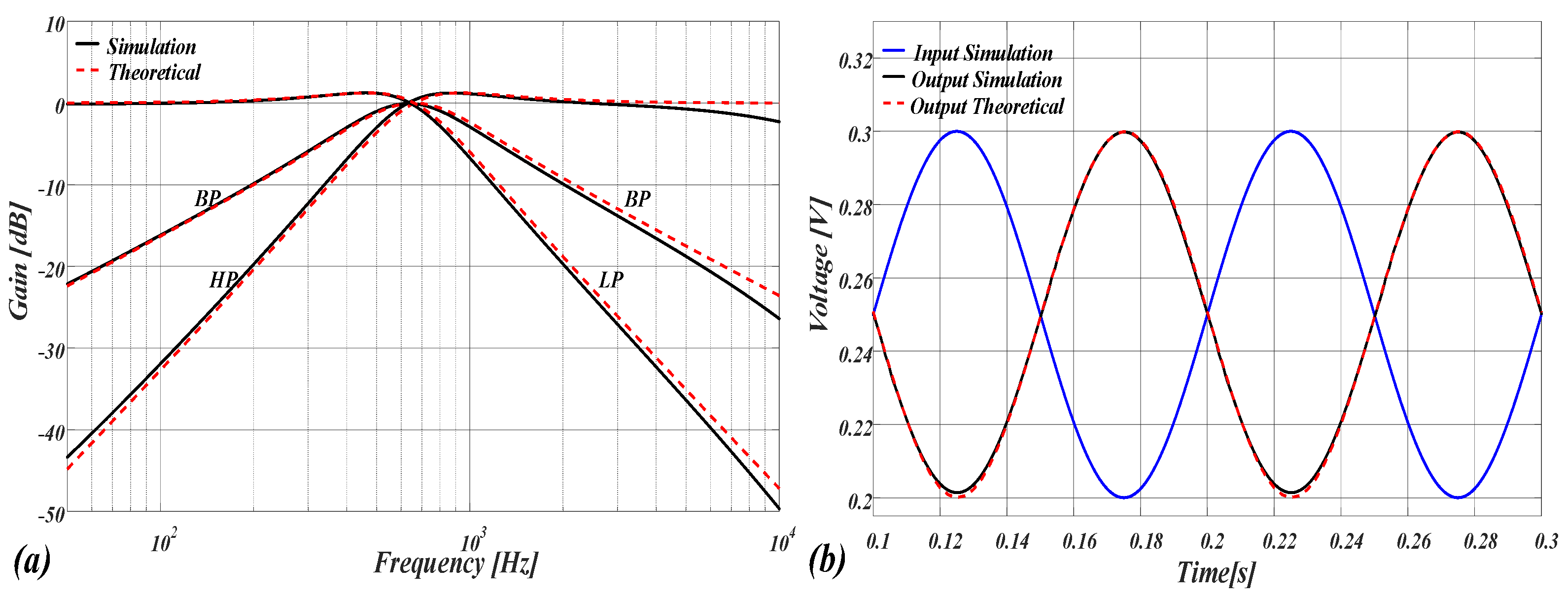
3.1. Proposed Gm-C Structure
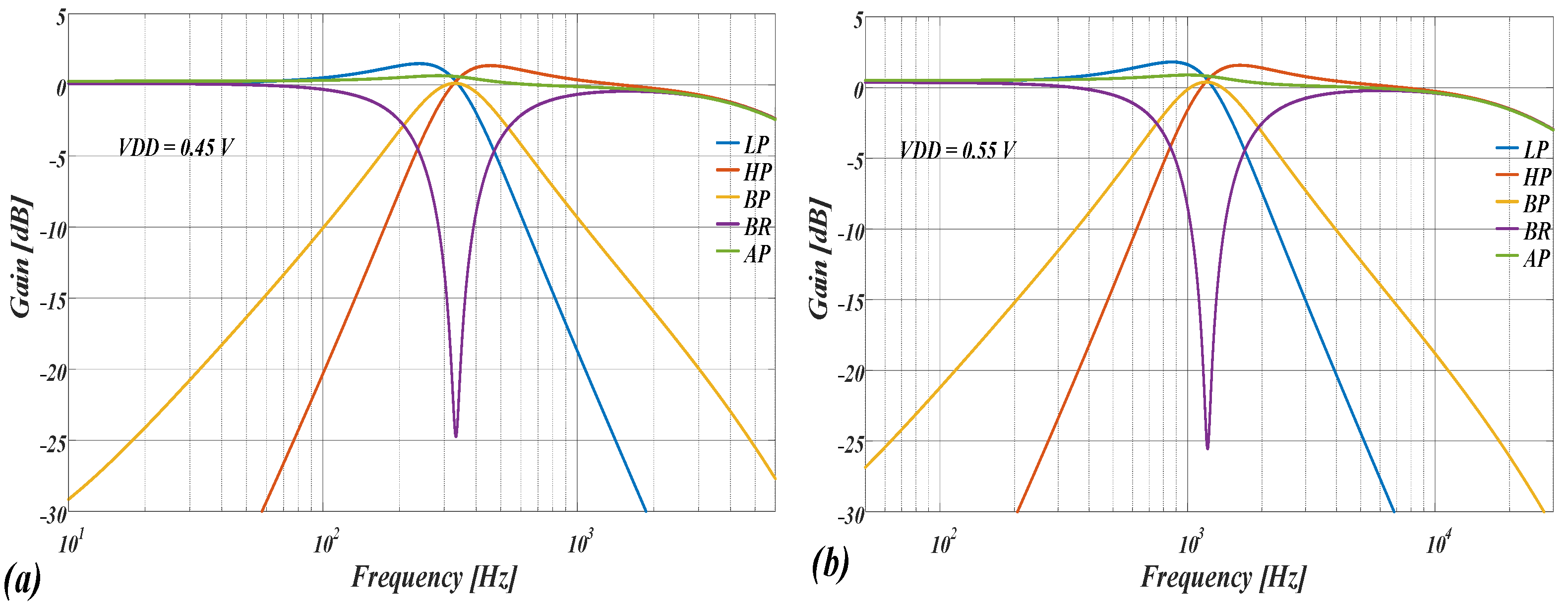
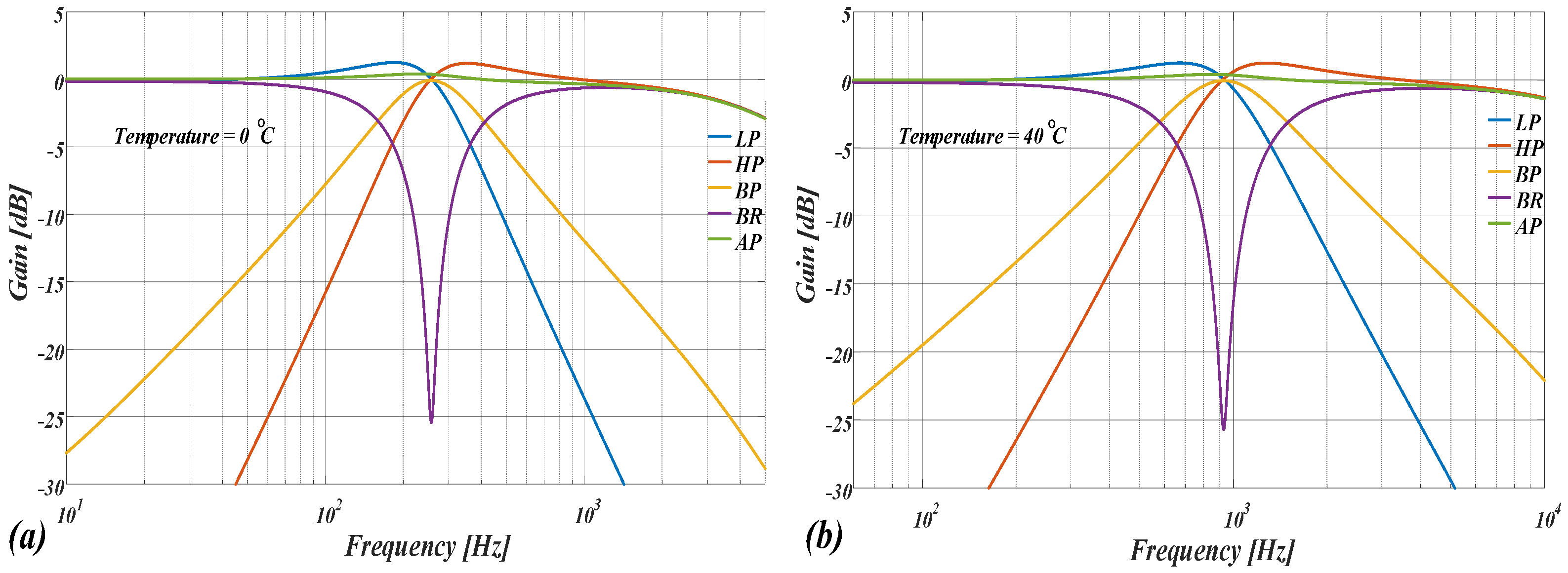
3.2. PVT Analysis
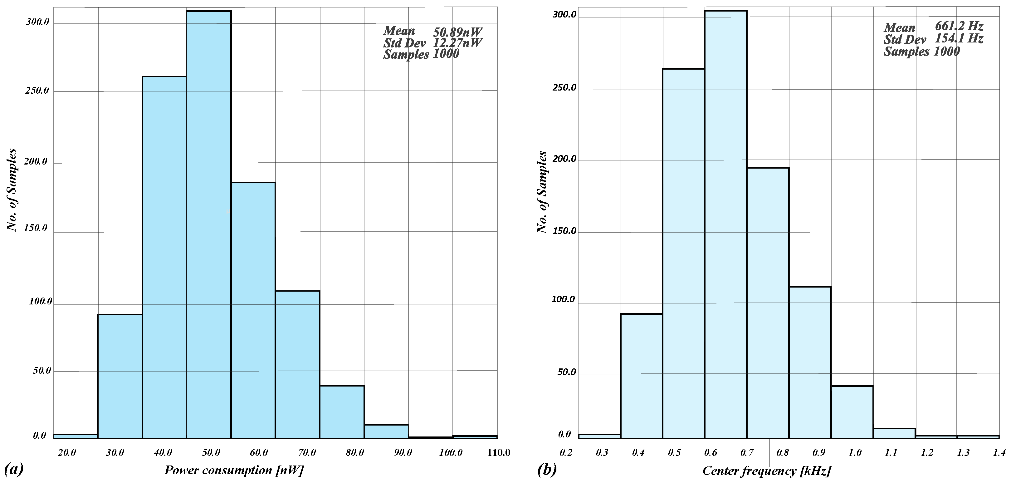
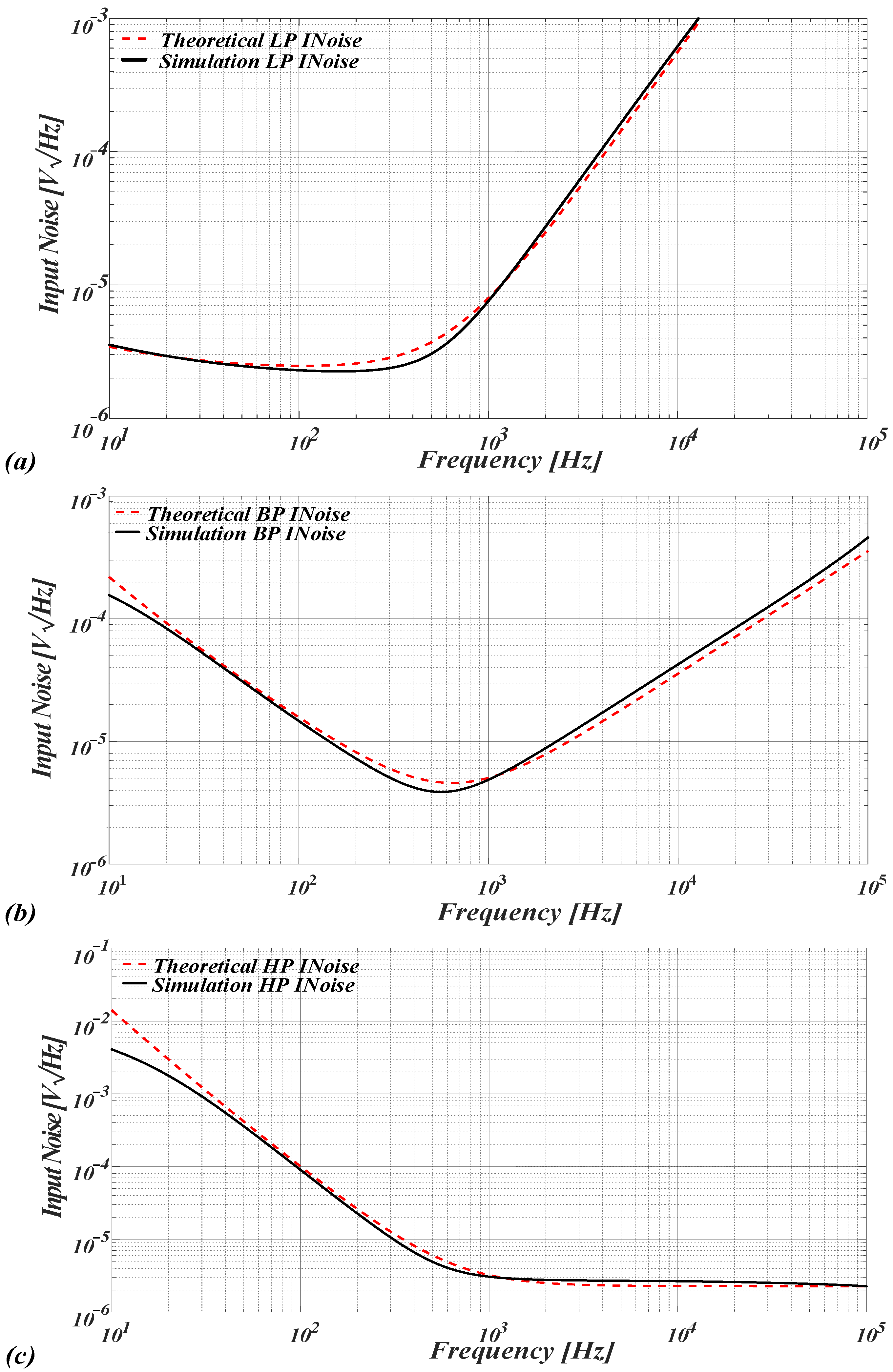
4. Noise Analysis
5. Comparison with State-of-the-Art
6. Conclusions
Author Contributions
Funding
Data Availability Statement
Conflicts of Interest
Abbreviations
| TSMC | Taiwan Semiconductor Manufacturing Company |
| OTA | Operational Transconductance Amplifier |
| VM | Voltage-Mode |
| CM | Current-Mode |
| TCM | Transconductance Mode |
| TRM | Trans-Resistance Mode |
| LP | Low-Pass |
| HP | High-Pass |
| BP | Band-Pass |
| BR | Band-Reject |
| AP | All-Pass |
References
- Sun, C.-Y.; Lee, S.-Y. A Fifth-Order Butterworth OTA-C LPF with Multiple-Output Differential-Input OTA for ECG Applications. IEEE Trans. Circuits Syst. II 2018, 65, 421–425. [Google Scholar] [CrossRef]
- Mincey, J.-S.; Vidrios, C.-B.; Silva-Martinez, J.; Rodenbeck, C.-T. Low-Power Gm-C Filter Employing Current-Reuse Differential Difference Amplifiers. IEEE Trans. Circuits Syst. II 2017, 64, 635–639. [Google Scholar]
- Chen, H.-P.; Liao, Y.-Z.; Lee, W.-T. Tunable mixed-mode OTA-C universal filter. Analog Integr. Circuits Signal Process. 2009, 58, 135–141. [Google Scholar]
- Chiu, W.-Y.; Horng, J.W. High-Input and low-output impedance voltage-mode universal biquadratic filter using DDCCs. IEEE Trans. Circuits Syst. II 2007, 54, 649–652. [Google Scholar] [CrossRef]
- Khateb, F.; Kumngern, M.; Kulej, T.; Biolek, D. 0.5 V Differential Difference Transconductance Amplifier and Its Application in Voltage-Mode Universal Filter. IEEE Trans. Access 2022, 10, 43209–43220. [Google Scholar]
- Jaikla, W.; Khateb, F.; Kumngern, M.; Kulej, T.; Ranjan, R.-K.; Suwanjan, P. 0.5 V Fully Differential Universal Filter Based on Multiple Input OTAs. IEEE Trans. Access 2020, 8, 187832–187839. [Google Scholar]
- Kulej, T.; Kumngern, M.; Khateb, F.; Arbet, D. 0.5 V Versatile Voltage- and Transconductance-Mode Analog Filter Using Differential Difference Transconductance Amplifier. Sensors 2023, 23, 688. [Google Scholar] [CrossRef] [PubMed]
- Khateb, F.; Kumngern, M.; Kulej, T.; Akbari, M.; Stopjakova, V. 0.5 V, nW-Range Universal Filter Based on Multiple-Input Transconductor for Biosignals Processing. Sensors 2022, 22, 8619. [Google Scholar] [CrossRef] [PubMed]
- Khateb, F.; Kumngern, M.; Kulej, T. 0.5-V 281-nW Versatile Mixed-Mode Filter Using Multiple-Input/Output Differential Difference Transconductance Amplifiers. Sensors 2023, 24, 32. [Google Scholar]
- Khateb, F.; Kumngern, M.; Kulej, T. 58-nW 0.5-V mixed-mode universal filter using multiple-input multiple-output OTAs. IEEE Trans. Access 2023, 11, 130345–130357. [Google Scholar]
- Namdari, A.; Aiello, O.; Caviglia, D. A 0.5 V, 32 nW Compact Inverter-Based All-Filtering Response Modes Gm-C Filter for Bio-Signal Processing. J. Low Power Electron. Appl. 2024, 14, 40. [Google Scholar] [CrossRef]
- Abuelma’atti, M.T.; Bentrcia, A. A novel mixed-mode OTA-C universal filter. Int. J. Electron. 2005, 92, 375–383. [Google Scholar] [CrossRef]
- Abdelfattah, O.; Roberts, G.W.; Shih, I.; Shih, Y.-C. An Ultra-Low-Voltage CMOS Process-Insensitive Self-Biased OTA with Rail-to-Rail Input Range. IEEE Trans. Circuits Syst. I Regul. Pap. 2015, 62, 2380–2390. [Google Scholar] [CrossRef]
- Lopez-Martin, A.; Garde, M.-P.; Algueta-Miguel, J.-M.; Beloso-Legarra, J.; Carvajal, R.-G.; Ramirez-Angulo, J. Energy-Efficient Amplifiers Based on Quasi-Floating Gate Techniques. Appl. Sci. 2021, 11, 3271. [Google Scholar] [CrossRef]
- Rodovalho, L.-H.; Aiello, O.; Rodrigues, C.-R. Ultra-Low-Voltage Inverter-Based Operational Transconductance Amplifiers with Voltage Gain Enhancement by Improved Composite Transistors. Electronics 2022, 9, 1410. [Google Scholar] [CrossRef]
- Namdari, A.; Aiello, O.; Caviglia, D. 0.5 V 32 nW Inverter-Based Gm-C Filter for Bio-Signal Processing. In Proceedings of the 2024 IEEE International Symposium on Circuits and Systems (ISCAS), Singapore, 19–22 May 2024; pp. 1–5. [Google Scholar] [CrossRef]
- Namdari, A.; Aiello, O.; Caviglia, D.D. 0.7 V, 215 nW Tunable Universal Gm-C Filter. In Proceedings of the SIE 2024, Genoa, Italy, 26–28 June 2024; Lecture Notes in Electrical Engineering. Springer: Cham, Switzerland, 2025; Volume 1263, pp. 41–47. [Google Scholar]
- Lo, T.-Y.; Hung, C.-C. A 1 GHz Equiripple Low-Pass Filter With a High-Speed Automatic Tuning Scheme. IEEE Trans Very Large Scale Integr. (VLSI) Syst. 2011, 19, 175–181. [Google Scholar] [CrossRef]
- Ramesh, N.; Gaggatur, J.-S. A 0.6 V, 2nd order low-pass Gm-C filter using CMOS inverter-based tunable OTA with 1.114 GHz cut-off frequency in 90 nm CMOS technology. In Proceedings of the 2021 34th International Conference on VLSI Design and 2021 20th International Conference on Embedded Systems (VLSID), Guwahati, India, 20–24 February 2021; pp. 305–309. [Google Scholar]
- Deng, J.; Fu, Z.; Wang, Z.; Chen, D.; Tang, X.; Guo, J. Improved Nauta Transconductor for Wideband Intermediate-Frequency gm-C Filter. In Proceedings of the IEEE International Symposium on Circuits and Systems (ISCAS), Baltimore, MD, USA, 28–31 May 2017; pp. 1–4. [Google Scholar]
- Barthélemy, H.; Meillére, S.; Gaubert, J.; Dehaese, N.; Bourdel, S. OTA based on CMOS inverters and application in the design of tunable band pass filter. Analog Integr. Circuits Signal Process 2008, 57, 169–178. [Google Scholar] [CrossRef]
- Pirmohammadi, A.; Zarifi, M.H. A low power tunable Gm-C filter based on double CMOS inverters in 0.35 µm. Analog. Integr. Circuits Signal Process 2012, 71, 473–479. [Google Scholar] [CrossRef]
- Lo, T.-Y.; Kao, C.-S.; Hung, C.-C. A Gm-C continuous-time analog filter for IEEE 802.11 a/b/g/n wireless LANs. In Proceedings of the 2007 International Symposium on Signals, Circuits and Systems, Iasi, Romania, 13–14 July 2007; pp. 1–4. [Google Scholar]
- Pedro, M.; Galán, J.; Sanchez-Rodríguez, T.; Pennisi, M.; Jiménez, R.; Mũnoz, F.; Carvajal, R.G. A linear compact tunable transconductor for Gm-C applications. Analog Integr. Circuits Signal Process 2012, 72, 351–361. [Google Scholar] [CrossRef]
- Nauta, B. A CMOS transconductance-C filter technique for very high frequencies. IEEE J. Solid-State Circuits 1992, 27, 142–153. [Google Scholar] [CrossRef]
- Oliveira Filho, F.M.; Leyva Cruz, J.A.; Zebende, G.F. Analysis of the EEG bio-signals during the reading task by DFA method. Phys. A Stat. Mech. Its Appl. 2019, 5, 664–671. [Google Scholar] [CrossRef]
- Luo, J.; Liu, C.; Yang, C. Estimation of EMG-Based Force Using a Neural-Network-Based Approach. IEEE Access 2019, 7, 64856–64865. [Google Scholar]
- Bing, P.; Liu, W.; Wang, Z.; Zhang, Z. Noise Reduction in ECG Signal Using an Effective Hybrid Scheme. IEEE Access 2020, 8, 160790–160801. [Google Scholar] [CrossRef]
- Shariat, M.H.; Gazor, S.; Redfearn, D.P. Bipolar Intracardiac Electrogram Active Interval Extraction During Atrial Fibrillation. IEEE Trans Biomed. Eng. 2017, 64, 2122–2133. [Google Scholar] [PubMed]
- Noce, E.; Bellingegnia, A.D.; Ciancioa, A.L.; Sacchettib, R.; Davallib, A.; Guglielmellia, E.; Zollo, L. EMG and ENG-envelope pattern recognition for prosthetic hand control. J. Neurosci. Methods 2019, 311, 38–46. [Google Scholar] [PubMed]
- Lee, S.-Y.; Wang, C.-P.; Chu, Y.-S. Low-voltage OTA–C Filter with an Area- and Power-efficient OTA for Biosignal Sensor Applications. IEEE Trans Biomed. Circuit Syst. 2019, 13, 56–67. [Google Scholar]


| Filtering Function | Current Mode | Trans-Resistance Mode | Input |
| LP | Inverting | Non-Inverting | iin1 |
| HP | Inverting | Non-Inverting | iin3 |
| BP | Inverting | Non-Inverting | iin2 |
| BR | Inverting | Non-Inverting | iin1 = iin3 |
| AP | Inverting | Non-Inverting | iin1 = iin2 = iin3 |
| Filtering Function | Voltage Mode | Transconductance Mode | Input |
| LP | Inverting | Non-Inverting | vin1 |
| HP | Inverting | Non-Inverting | vin3 |
| BP | Inverting | Non-Inverting | vin2 |
| BR | Inverting | Non-Inverting | vin1 = vin3 |
| AP | Inverting | Non-Inverting | vin1 = vin2 = vin3 |
| Aspect Ratio of OTA and Bias Circuit | |
|---|---|
| Transistor | W/L (µm/µm) |
| MP,INV | 5/3 |
| MN,INV | 1/3 |
| MB1, MB2 | 1/0.18 |
| Specifications | Value |
|---|---|
| Supply voltage [V] | 0.5 |
| DC gain [dB] | 41.3 |
| Phase margin [°] | 90 |
| 11.67 | |
| 1.24 | |
| 1.24 | |
| THD [%] | 1 |
| 13.82 | |
| 13.72 | |
| 13.77 | |
| 242 | |
| 4.69 | |
| CL [pF] | 1 |
| C1 = C2 = 20 pF C3 [pF] | Quality Factor (Q) |
|---|---|
| 20 | 1 |
| 40 | 2 |
| 60 | 3 |
| Capacitance Values [pF] | Frequency Range [Hz] |
|---|---|
| C1 = C2 = C3 = 10 | 1270 |
| C1 = C2 = C3 = 30 | 423 |
| C1 = C2 = C3 = 80 | 158 |
| C1 = C2 = C3 = 250 | 50.6 |
| Type of Signal | Frequency Range [Hz] | Suitability of the Proposed Filter |
|---|---|---|
| EEG | 0.5–60 | Yes |
| EMG | 10–200 | Yes |
| ECG | 0.05–250 | Yes |
| IEGM | 0.7–70 | Yes |
| ENG | 250–5000 | Yes |
| Parameter | SS | SF | FS | FF | TT |
|---|---|---|---|---|---|
| OTA’s gain [dB] | 41.4 | 42.4 | 41.4 | 41 | 41.3 |
| OTA’s phase [°] | 90 | 90 | 90 | 90 | 90 |
| Filter’s power consumption [nW] | 20.96 | 58.18 | 71.64 | 108.3 | 48 |
| Filter’s center frequency [Hz] | 282.5 | 736 | 755 | 1400 | 635 |
| Parameter | 0.45 V | 0.5 V | 0.55 V |
|---|---|---|---|
| OTA’s gain [dB] | 41 | 41.3 | 42.9 |
| OTA’s phase [°] | 90 | 90 | 90 |
| Filter’s power consumption [nW] | 23.12 | 48 | 101.8 |
| Filter’s center frequency [Hz] | 331 | 635 | 1200 |
| Parameter | 0 °C | 10 °C | 20 °C | 30 °C | 40 °C |
|---|---|---|---|---|---|
| OTA’s gain [dB] | 41.5 | 41.4 | 41.3 | 41.2 | 41.1 |
| OTA’s phase [°] | 90 | 90 | 90 | 90 | 90 |
| Filter’s power consumption [nW] | 18.22 | 26.6 | 38 | 53.2 | 73.12 |
| Filter’s center frequency [Hz] | 256 | 365.6 | 510.5 | 695 | 929 |
| Parameter | 0.5 V | 0.6 V | 0.7 V | 0.8 V | 0.9 V | 1 V | 1.1 V | 1.2 V |
|---|---|---|---|---|---|---|---|---|
| W] | 0.048 | 0.22 | 1.067 | 4.36 | 13.46 | 32.95 | 67.25 | 121 |
| Center frequency [kHz] | 0.635 | 2.244 | 7.413 | 21.83 | 52 | 96.83 | 150.7 | 211 |
| Parameter | Mean | Std Dev |
|---|---|---|
| OTA-DC gain [dB] | 40.24 | 0.17 |
| OTA-Phase margin [°] | 90.5 | 0.012 |
| OTA-GBW [kHz] | 12.65 | 3 |
| OTA-Input Noise | 1.23 | 0.145 |
| OTA-Output Noise | 1.29 | 0.153 |
| OTA-THD [%] | 1.18 | 0.2 |
| OTA- | 14.28 | 0.466 |
| OTA- | 14.04 | 0.435 |
| OTA- | 14.16 | 0.317 |
| OTA-Output voltage | 240.5 | 12 |
| OTA-Power consumption | 4.88 | 1 |
| Filter-Power consumption | 50.89 | 12.27 |
| Filter-Center frequency [Hz] | 661.2 | 154.1 |
| Parameter | Unit | Parameter | Unit |
|---|---|---|---|
| K | KN | ||
| T | COX | ||
| γ | 1 | L)P | |
| 35.6 nS | L)N | ||
| 47.4 nS | C1 = C2 = C3 | 20 pF | |
| KP | gm | 83 nS |
| Frequency Range [Hz] | Capacitance Value [pF] | TT | SS | SF | FS | FF |
|---|---|---|---|---|---|---|
| Pre-layout | 250 | 50.6 | 22.5 | 58.7 | 60.2 | 111 |
| Post-layout | 48.3 | 21.6 | 56 | 53.3 | 107 | |
| Pre-layout | 80 | 158 | 70.3 | 183.6 | 188.3 | 349 |
| Post-layout | 151.3 | 67.4 | 175 | 166.7 | 333.4 | |
| Pre-layout | 30 | 423 | 188 | 491 | 502.3 | 933 |
| Post-layout | 404.5 | 180.3 | 469 | 444.6 | 891 | |
| Pre-layout | 20 | 635 | 282.5 | 736 | 755 | 1400 |
| Post-layout | 608 | 271 | 705 | 667 | 1342 | |
| Pre-layout | 10 | 1270 | 566 | 1479 | 1513 | 2812 |
| Post-layout | 1222 | 547 | 1412 | 1336 | 2691 |
| Frequency Range [Hz] | Capacitance Value [pF] | 0.5 V | 0.45 V | 0.55 V |
|---|---|---|---|---|
| Pre-layout | 250 | 50.6 | 26.36 | 95 |
| Post-layout | 48.3 | 25.6 | 91.4 | |
| Pre-layout | 80 | 158 | 82.4 | 297 |
| Post-layout | 151.3 | 80.16 | 286 | |
| Pre-layout | 30 | 423 | 220 | 792.5 |
| Post-layout | 404.5 | 214.8 | 762 | |
| Pre-layout | 20 | 635 | 331 | 1200 |
| Post-layout | 608 | 323 | 1145 | |
| Pre-layout | 10 | 1270 | 663.7 | 2376 |
| Post-layout | 1222 | 648.6 | 2296 |
| Frequency Range [Hz] | Capacitance Value [pF] | 27 °C | 0 °C | 10 °C | 20 °C | 30 °C | 40 °C |
|---|---|---|---|---|---|---|---|
| Pre-layout | 250 | 50.6 | 20.3 | 29 | 40.5 | 55 | 74 |
| Post-layout | 48.3 | 19 | 27.5 | 38.7 | 53 | 71 | |
| Pre-layout | 80 | 158 | 63.7 | 91 | 127 | 173.4 | 231 |
| Post-layout | 151.3 | 59.7 | 86.3 | 121 | 166 | 222 | |
| Pre-layout | 30 | 423 | 170.2 | 243.2 | 339.6 | 463.4 | 618 |
| Post-layout | 404.5 | 159.6 | 230.6 | 323.6 | 443.6 | 594.3 | |
| Pre-layout | 20 | 635 | 256 | 365.6 | 510.5 | 695 | 929 |
| Post-layout | 608 | 240 | 346.7 | 486.4 | 667 | 893 | |
| Pre-layout | 10 | 1270 | 513 | 733 | 1021 | 1393 | 1862 |
| Post-layout | 1222 | 482 | 696.6 | 979.5 | 1340 | 1794 |
| Specifications | This Work | [5] | [6] | [7] | [8] | [9] | [10] |
|---|---|---|---|---|---|---|---|
| Supply voltage [V] | 0.5 | 0.5 | 0.5 | 0.5 | 0.5 | 0.5 | 0.5 |
| Supply voltage scalability | 0.5V to 1.2V | No | No | No | No | No | No |
| Universal | Yes | Yes | Yes | Yes | Yes | Yes | Yes |
| Multi-mode | Yes | No | No | Yes | No | Yes | Yes |
| Frequency tuning by current bias | No | Yes | Yes | Yes | Yes | Yes | Yes |
| Filter order | 2 | 2 | 2 | 2 | 2 | 2 | 2 |
| Center frequency [Hz] | 635 | 254 | 10 | 323 | 153 | 211 | 114 |
| Frequency tuning range [Hz] | 50.6–1270 | 66–501 | 5.9–21.6 | 162–1330 | 62.3–595.6 | 28–211 | 58.8–840 |
| Tuning range [X] | 25 | 7.6 | 3.66 | 8.2 | 9.56 | 7.53 | 14.28 |
| THD [%] @ amplitude [mVP] | 0.93 @ 50 | 0.62 @ 50 | 1 @ 50 | 0.8 @ 50 | 0.33 @ 50 | 1 @ 150 | 1 @ 135 |
| Dynamic range [dB] | 53.46 | 49.7 | 63 | 53.2 | 50 | 58.23 | 53.2 |
| R.M.S output noise [µVrms] | 75 | 116 | 45 | 108 | 220 | 130 | 208 |
| Power consumption [nW] | 48 | 616 | 53.3 | 646 | 37 | 281 | 58 |
| ] | 2.795 | - | - | - | 11.537 | - | - |
| ] | 0.08 | 3.96 | 1.88 | 2.187 | 2.41 | 0.816 | 0.556 |
Disclaimer/Publisher’s Note: The statements, opinions and data contained in all publications are solely those of the individual author(s) and contributor(s) and not of MDPI and/or the editor(s). MDPI and/or the editor(s) disclaim responsibility for any injury to people or property resulting from any ideas, methods, instructions or products referred to in the content. |
© 2025 by the authors. Licensee MDPI, Basel, Switzerland. This article is an open access article distributed under the terms and conditions of the Creative Commons Attribution (CC BY) license (https://creativecommons.org/licenses/by/4.0/).
Share and Cite
Namdari, A.; Aiello, O.; Dolatshahi, M.; Caviglia, D.D. A 48 nW, Universal, Multi-Mode Gm-C Filter with a Frequency Range Tunability. Electronics 2025, 14, 1334. https://doi.org/10.3390/electronics14071334
Namdari A, Aiello O, Dolatshahi M, Caviglia DD. A 48 nW, Universal, Multi-Mode Gm-C Filter with a Frequency Range Tunability. Electronics. 2025; 14(7):1334. https://doi.org/10.3390/electronics14071334
Chicago/Turabian StyleNamdari, Ali, Orazio Aiello, Mehdi Dolatshahi, and Daniele D. Caviglia. 2025. "A 48 nW, Universal, Multi-Mode Gm-C Filter with a Frequency Range Tunability" Electronics 14, no. 7: 1334. https://doi.org/10.3390/electronics14071334
APA StyleNamdari, A., Aiello, O., Dolatshahi, M., & Caviglia, D. D. (2025). A 48 nW, Universal, Multi-Mode Gm-C Filter with a Frequency Range Tunability. Electronics, 14(7), 1334. https://doi.org/10.3390/electronics14071334