Abstract
For the waveguide coil in a High-Power Microwave (HPM) source, a strong repetitive Flat-top Pulsed Magnetic Field (FTPMF) is needed, which requires the power supply system to generate a high load current (3∼5 kA) with high stability (<1000 ppm) and a long pulse-width (15∼20 ms). To achieve this, this article proposes a novel topology which includes a capacitor bank as the main power supply to guarantee a long pulse-width, combined with an active current compensator to regulate the load current precisely. A PI control scheme with slope compensation is used to solve the current fluctuation caused by capacitor switching. The novel topology also features a fast rising and falling time, thus it is suitable for repetitive working applications. The parameters of the topology are calculated by analysis to guarantee the working condition of a 45 GHz HPM source, and the operating principle of this topology is verified through low-power-scale experiments.
1. Introduction
High-power microwaves (HPM) refer to electromagnetic waves with a frequency range of 1 GHz to 300 GHz and a peak power exceeding 100 MW [1], which play important roles in civilian and military fields such as plasma heating, high-energy particle acceleration, and high-power radar. For the generation of HPM pulses, the plasma beam of the HPM source needs to be restrained and guided by a waveguide coil [2,3,4], and the magnetic field of the coil needs to be strong and stable during the period when the beam passes through it.
For such applications, permanent magnets cannot generate a strong enough magnetic field to meet the demands. Superconducting magnets, although capable of generating enough strong and stable magnetic fields, require a cryogenic system that is quite large in volume and quite difficult to maintain. A Pulse Magnetic Field system has a much smaller volume and can also generate a large enough field intensity to meet the demand, but the pulse width is not enough. The Flat-top Pulsed Magnetic Field (FTPMF) system combines the advantages of the above magnetic systems, i.e., high stability, high field strength, a relatively long pulse-width and a much smaller volume, which makes it suitable for this application. In addition, it can be widely used in nuclear magnetic resonance (NMR) [5], the magnetic field immunity test [6], terahertz [7], the magnetic confinement of Tokamak [8] and other scientific research and industrial application fields that require a high magnetic field with a relatively long pulse-width.
In recent studies, there are mainly four types of power supply systems for a FTPMF according to their energy storage type: the city power grid with a rectifier [9], the pulse generator with a rectifier [10], the battery bank [11], and the capacitor bank [12]. TU Vienna used a high-power rectifier set which is connected to the city’s main power grid to achieve a FTPMF of 25 T (13 kA)/100 ms with a stability of 15% ripple [9], but this kind of power supply will cause impact and a lot of harmonic pollution to the power grid. A pulse generator can easily support a FTPMF with a very long duration (>100 ms) due to its high energy storage density without polluting the power grid, but it is very expensive to make and to maintain. A 50 T/100 ms FTPMF with a stability of 5000 PPM was achieved at the Wuhan National Magnetic Field Center (WHMFC) by a 100 MVA/100 MJ generator with a 135 MW rectifier [10]. The battery bank can provide very high stability because of its stable output voltage, but the rising time of the load current is very long due to the limitation of the chemical reaction rate inside the battery. This leads to an undesirable temperature rise for the load coil, which will reduce the system’s repetition frequency since it will take more time for the load coil to cool down. A 23.37 T/100 ms FTPMF with a stability of 65 PPM was achieved at the WHMFC by a battery bank with a bypass circuit of IGBTs operating in the active region [11], but the rising time of it is up to 100ms. A capacitor bank is the most commonly used main power supply for the FTPMF due to its low cost, fast current rising rate and modular structure, which makes it the most suitable choice for HPM source applications. At the Laboratory for Space Environment and Physical Sciences in China, a 26 kA/12 ms flat-top current was achieved by a capacitor bank based on an optimized sequentially fired pulse-forming network (SFPFN) scheme with a short rising time of less than 1ms, but its ripple was up to 15% due to an open-loop control scheme and there being no current regulation [12]. All of the above FTPMF systems are shown in Table 1.
Table 1.
Statistics of Different FTPMF Systems.
The guiding coil in high-power microwave (HPM) source systems demands a pulsed current supply with the following specifications:
- (a).
- Peak current: 3∼5 kA;
- (b).
- Rising/falling edge duration: <5 ms (to minimize Joule heating and ensure high repetition rates);
- (c).
- Flat-top duration: ∼20 ms (non-critical);
- (d).
- Current stability/accuracy: ≤1000 ppm.
As summarized in Table 1, existing power supply architectures fail to meet these requirements:
- (a).
- City grid + rectifier: Unacceptable grid harmonics and ripple (15%).
- (b).
- Pulse generator + rectifier: Prohibitively high cost, limited stability (5000 ppm) and slow current rise (>100 ms).
- (c).
- Battery bank: Slow current rise (>100 ms) due to electrochemical inertia.
- (d).
- Capacitor bank in the form of an optimized SFPFN: Fast current rise rate (<2 ms rise time) but slow fall rate (>10 ms) and unacceptably high ripple ().
To address these challenges, we propose a modified capacitor bank system based on the optimized SFPFN, augmented with three critical innovations: fast current decay circuitry to accelerate the current fall rate, an active current compensator (ACC) to compensate for the current ripple and close-loop PI control with slope compensation to improve the current stability to the specification of 1000 ppm. This hybrid architecture combines the inherent advantages of capacitor banks (modularity, low cost, and sub-millisecond rise time) with enhanced dynamic control capabilities. The proposed design resolves the historical trade-off between speed and precision in capacitor-based systems, positioning it as a scalable solution for high-repetition HPM applications.
To facilitate a more intuitive comparison of the performance differences among these various power supply schemes, the current waveforms of each configuration from Table 1 are depicted in Figure 1. For consistency and ease of comparison, both the load conditions and the peak current values have been normalized across all schemes. It is evident from Table 1 that the optimized SFPFN topology achieves the shortest current rise time under its original load conditions. However, in the normalized current waveforms, the proposed topology exhibits a faster rise time than the optimized SFPFN. This discrepancy arises from the significant difference in load inductance between the two configurations: the optimized SFPFN operates with a 40 H load inductance, whereas the proposed topology employs a 1 mH load. When normalized to equivalent load conditions, the proposed topology demonstrates superior transient performance in terms of rise time. A detailed comparative analysis of these results is provided in Section 4 (Simulation Results), including waveform comparisons and quantitative evaluations.
Figure 1.
Normalized current waveforms of different schemes.
This article is organized as follows. In Section 2, a proposed current source topology based on an optimized SFPFN is introduced to generate a flat-top current, and the operating principle of the proposed topology is analyzed. In Section 3, the parameter design of the topology and the control scheme which includes a slope compensation are studied in consideration for the stability and rising/falling time requirements of the HPM source. In Section 4, simulation results are presented in order to compare different control schemes. In Section 5, a low-power-scale experimental platform is built to validate the operating principle of the proposed topology and the slope compensation control scheme. Section 6 summarizes the conclusions drawn from this study.
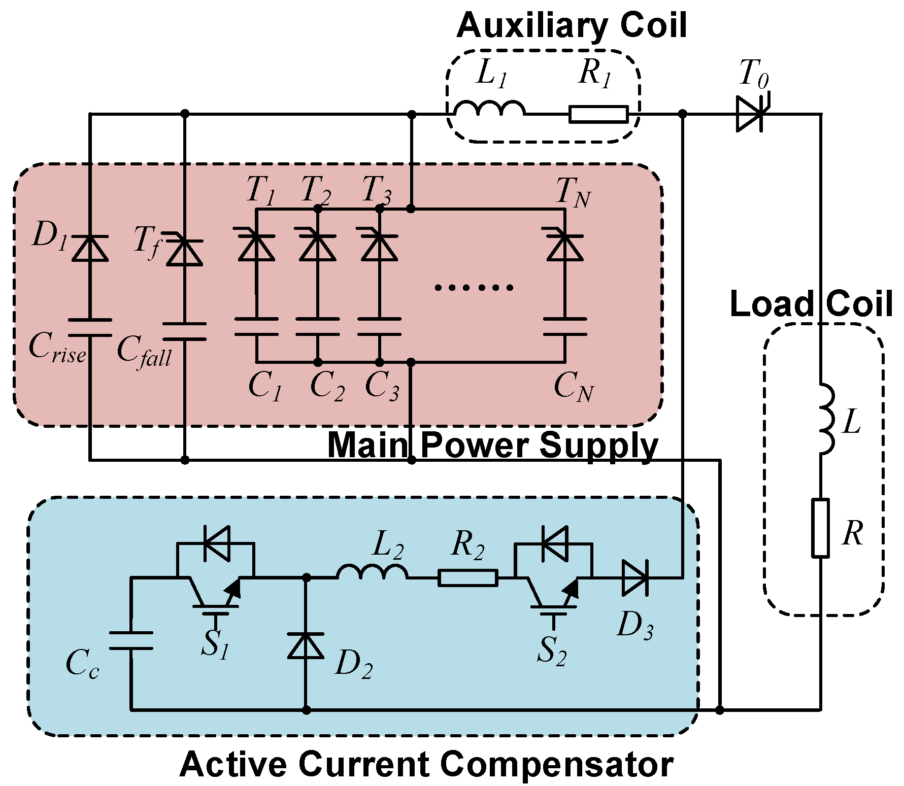
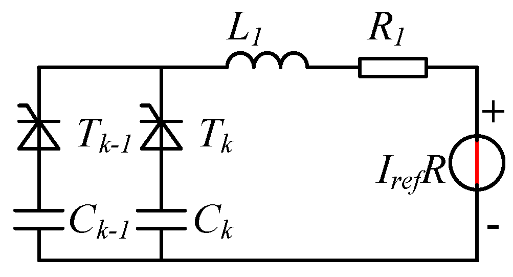
2. Proposed Current Source Topoplogy Based on an Optimized SFPFN
2.1. Original Optimized SFPFN with Open-Loop Control Scheme
An SFPFN is a kind of topology meant for generating a high-level pulsed flat-top current in resistive loads. In [12], optimizing work has been made for this topology to be applied to a heavily inductive load, as in the HPM source application. The optimized SFPFN topology is depicted in Figure 2. And, the waveform of the current is shown in Figure 3.
Figure 2.
Schematic of the optimized SFPFN.
Figure 3.
Current waveform of the optimized SFPFN.
The optimized SFPFN consists of multiple modules in which a capacitor is connected in series with a thyristor. C1 to CN are capacitors charged with initial voltages of
to , and T1 to TN are thyristors corresponding to each capacitor that are sequentially triggered at time to . As depicted in Figure 3, the ripple is not acceptable for HPM application as its ripple is higher than 15% due to a lack of compensation.
2.2. Proposed Topology
The topology of the power supply system is depicted in Figure 4, which is composed of a main power supply structure based on an optimized SFPFN, an ACC structure using IGBTs as switches, an auxiliary coil and the load coil. The main power supply structure is composed of a series of capacitors with different capacitance and voltage levels. Specifically, the of a small capacitance and a high initial voltage is used to generate a fast-rising current stage, a capacitor bank from to of a big capacitance and a low initial voltage are used to maintain the flat-top current stage, and the of a small capacitance and a high voltage is used to generate a fast-falling current stage. The ACC structure compensates for the current shortage during the platform stage of the load current and the regulating of the load current to minimize the ripple, and a PI controller is used to change the duty cycle of the ACC’s switch . An auxiliary coil is connected between the main power supply structure and load coil, which works as a voltage filter and shared part of the voltage to reduce the switching stress of the ACC’s switch. Moreover, it also determines the current ripple of the main power supply structure, which will be discussed in a later part of this section.
Figure 4.
Schematic of the proposed power supply topology for an HPM.
Figure 5 depicts the expected theoretical load current waveform and the output voltage waveform of the main power supply, which are divided into a rising stage, a flat-top stage and a falling stage. In Figure 5, is the load current, is the output current of the main power supply structure and is the output current of the ACC structure.
Figure 5.
Theoretical load current waveform and output voltage.
To effectively capture the steady-state, transient, and switching behaviors of the system, as well as analyzing the operating points and stability, a state trajectory analysis is introduced in this paper.
State trajectory analysis is a common analytical tool in the field of power electronics, particularly for studying the dynamic behavior and steady-state performance of nonlinear systems. Based on the state-space model, it integrates circuit topology and system parameters to describe power electronic circuits. For this topology, the current of the auxiliary coil L1 is chosen and normalized as the resonance current , and the voltage of the capacitors in the main power supply structure is chosen and normalized as the the resonance voltage . The state trajectory of the system can be illustrated as in Figure 6.
Figure 6.
State trajectory of the proposed topology.
The operating principles of the topology are as follows.
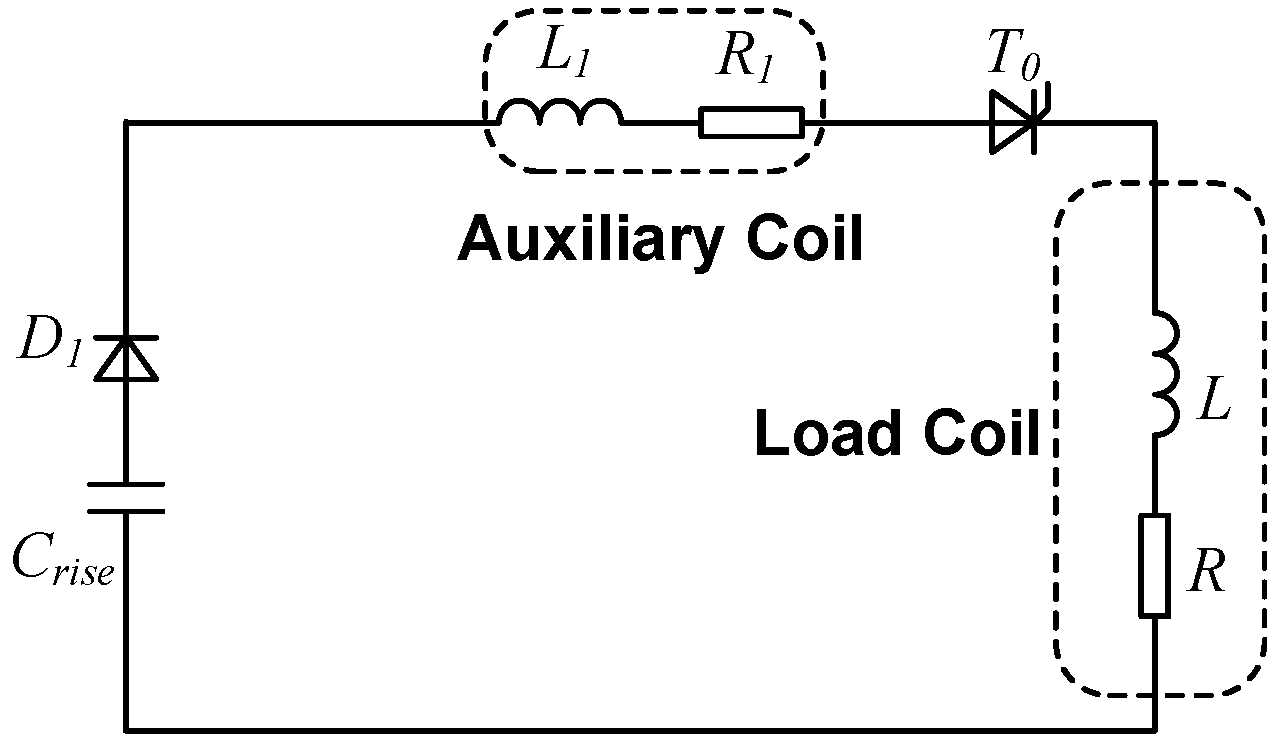
2.2.1. Mode 1: Rise Mode
The first mode of a complete pulse is the rise mode, and the equivalent circuit is shown as Figure 7. is turned on at , and the capacitor is connected to the circuit through , then a first-order series LCR circuit is formed with the rising stage capacitor , the load coil L and R and the auxiliary coils and .
Figure 7.
Equivalent circuits of rise mode.
During the rise mode, the differential equation of the circuit can be written as
In (1), is the load current. (1) can be solved as
In (2), , is the initial voltage of the rising stage capacitor .
Ideally at , the current rises to the maximum value which equals , the reference value of the flat-top current. In the state trajectory, the procedure is from point A to point E.
can be obtained by finding the zero point of the derivative of (2), and the result is:
At , the load curent reaches the peak value , which means that
But, in a practical situation, Equation (4) cannot be satisfied precisely. Therefore, is typically set that is slightly lower than the ideal value to ensure that the maximum current does not exceed the reference value. And in the state trajectory, the procedure is from point to point .
2.2.2. Mode 2: Flat-Top Mode
During the flat-top mode, the equivalent circuit is shown as Figure 8. and are turned on at , and PWM signals are transmitted to . When detecting that the output current of the rising stage capacitor has dropped to the designed minimum value as shown in Figure 5, which is from point to point in Figure 6, will be turned on and will bear an inverse voltage and be blocked. And then, the load coil will be powered by both the capacitor bank in the main power supply structure and the ACC structure, which is from point to point C in Figure 6. As the voltage of one capacitor in the capacitor bank drops, which is from point C to point E then to point D in Figure 6, to will be successively turned on according to the calculated time interval , and a new capacitor will be switched on, as from point D to point C in Figure 6. Because the voltage of the capacitor connected to the newly turned-on thyristor is higher than the voltage of the previously discharged capacitor, the thyristor connected to the previously discharged capacitor can be forcibly turned off by bearing an inverse voltage.
Figure 8.
Equivalent circuits of flat-top mode.
During this mode, due to the large capacitance of each capacitor in the capacitor bank, the ripple of the current provided by the capacitor bank is fairly small, and the ACC structure only needs to provide a small amount of current to supplement it, which means that the thyristors bear most of the current and voltage stress, while the high-frequency semiconductor switches in the ACC structure only need to bear a much smaller current and voltage stress.
The current fluctuation of the main power supply structure is decided by the capacitance of one capacitor branch of the capacitor bank i.e., , inductance and resistance of the auxiliary coil and the discharge interval, i.e., . Since the current of the inductive load at the flat-top stage is constant with very small ripples, meaning , the voltage of the load can be described as (5).
This means that the load can be regarded as equivalent to a constant voltage source. The equivalent circuit of the topology is depicted in Figure 9.
Figure 9.
Simplified equivalent circuit when studying the current fluctuation of the main power supply.
The discharge process of a single capacitor branch is analyzed, and the voltage waveform of the capacitor branch and the current waveform flowing through are depicted in Figure 10. Ideally, the maximum current value of the main power structure , i.e., , is designed to be equal to the reference value of the flat-top current , meaning . The differential equation of the circuit is
Figure 10.
Sketch of waveforms of the main power supply.
In (6), is the voltage of . Since the capacitance of the capacitor branch is large and the fluctuation of the current is small (normally designed to be smaller than 2%), in (6) can be replaced by its median value , and can be regarded as dropping linearly, which is
In (7), is the initial voltage of every capacitor branch in the capacitor bank.
At the time , the current of the main power supply structure reaches the peak value, which means that
By combining (6), (7) and (8), the current fluctuation of the main power supply assumed as can be solved as
And, the initial voltage of every capacitor branch in the capacitor bank can be solved as
is the maximum value of the current that the ACC needs to compensate for, which can be used to evaluate the output power level of the ACC. From (9), we can see that raising the inductance of the auxiliary coil can help lower the current fluctuation of the main power supply while the load inductance has no influences on it.
2.2.3. Mode 3: Fall Mode
Most FPTMF topologies care little about this stage and choose a crowbar branch to let the load current drop slowly in an LR-damping process as in Figure 3. But in the proposed topology, an accelerated fall mode is introduced with the fall mode capacitor, and the equivalent circuit is shown as Figure 11. After the load current reaches the reference pulse-width, the PWM signal of will be turned off. After the output current of the ACC drops to 0, will be turned off and then will be turned on, and the falling stage capacitor with a small capacitance and a high voltage will be connected to the circuit. The thyristors of the capacitor bank will bear an inverse voltage and be shut down. After the voltage of drops until it is lower than the voltage of , a first-order series LCR circuit consisting of the rise mode capacitor Crise, the load coil L and R and the auxiliary coils and will be formed, so that the load current will rapidly drop to 0, which is from point E to point F in Figure 6.
Figure 11.
Equivalent circuits of fall mode.
3. Parameter Design and Controller Design
3.1. Ripple of the Output Current of the ACC
The ripple of the output current of the ACC is a direct factor affecting the quality of the final load current, namely the stability of the flat-top current. Its decision formula is derived as follows.
The switching frequency of in the ACC is very high (up to several kHz), and the capacitance of the capacitor bank, i.e., , along with the ACC’s bus capacitor, i.e., CC, are both very large. During a switching cycle, the voltage of the ACC can be seen as constant, which can be regarded as a voltage source. Therefore, the circuit in the flat-top mode can be further simplified as shown in Figure 12.
Figure 12.
Simplified equivalent circuit when studying the ripple of the output current of the ACC.
in (12) is a switching function. When turns on, ; when turns off, . in (11) is the voltage of the ACC’s bus capacitor .
In (14), The current change rate of the output current of the ACC can be solved according to Davinen’s theorem as
When turns on,
When turns off,
Similarly, the change rate of the load current iload can also be derived according to Davinen’s theorem.
For the ACC to work properly, its minimum current change rate should be greater than the maximum current change rate of the main power supply structure . It can be seen from Figure 10 that reaches the maximum current change rate when the capacitor bank switches to a new capacitor. The maximum change rate of current is
Figure 13.
Sketch of the change rate of and .
Assuming that the switching frequency of is , the theoretical maximum fluctuation of the current (also of ) happens when the output current of the main power supply structure reaches its minimum value, which is also the same time when the capacitor bank switches to a new capacitor. At this moment, the change rate of the will instantly change from a negative value to a positive value, and due to the control scheme based on the fixed switching frequency and the changeable duty cycle, the output current of the ACC will be one switching period later than the expected current that needs to be compensated for, i.e., . Figure 14 depicts the situation. It can be seen that the output current of the ACC will increase at its maximum change rate through nearly a whole switching period (because the change rate of also reaches its maximum value at this moment) right after the current sensor captures the peak value of . The maximum fluctuation of the load current can be calculated as
Figure 14.
Situation when the iACC has the theoretical maximum amount of fluctuation.
From (22), we can see that under the condition of satisfying (20) and (21), lowering the capacitor bank’s initial voltage or the ACC’s bus capacitor initial voltage can help lower the fluctuation of the load current, thus improving the load current’s stability. And, increasing the switching frequency is the most efficient way to improve the load current’s stability.
3.2. Parameter Design for the Topology
For a 45 GHz HPM plasma source, the parameter ranges of the waveguide coil are shown in Table 2 (derived from Finite Element Simulation results by COMSOL 5.4).
Table 2.
Parameters for a 45 GHz HPM plasma source’s waveguide coil.
Firstly, choose the load current of 4 kA, the load inductance and resistance of 1 mH and 100 mΩ, the flat-top duration, i.e., the pulse-width, of 20 ms, the rising time and falling time of 4 ms, the main power suply output current fluctuation of 6%, and the stability along with the precision both of within 1000 ppm.
Then, the capacitance of the is restrained by the rise mode time, which refers to (3) and the value is chosen as 1200 F, and the initial voltage of the is restrained by (4) and chosen as 6100 V. The capacitance of each capacitor in the capacitor bank, i.e., , is chosen as 100 mF because of manufacturing restraints. The discharge interval of the , i.e., , is restrained by the the current fluctuation of the main power supply, which refers to (9). According to a 6% fluctuation in the main power supply output current, the is chosen to be 4 ms, and as the flat-top duration is set to be 20 ms, six capacitors are needed. And, the initial voltage of each capacitor in the capacitor bank is restrained by (10), and can be derived as 957 V. The rest parameters are all key factors that influence the ripple of the ACC as discussed in Section 3.1, and the boundaries are defined by (20) and (21). And, a set of parameters that meet the boundaries is listed in Table 3.
Table 3.
Designed parameters of the topology.
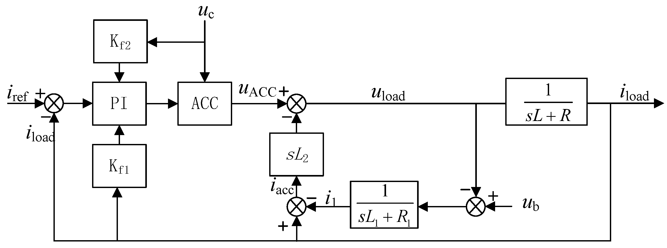
3.3. Controller Design with Slope Compensation
Figure 15 shows the closed-loop control diagram of the proposed current source topology in the flat-top mode. The controller contains a proportional-integral (PI) controller with two feed-forwards, i.e., the capacitor bank voltage feed-forward and the ACC bus voltage feed-forward. The voltage feed-forward loops are needed to correct the disturbance introduced by the voltage drop of the capacitor bank, which is one of the main causes of the load current fluctuations. However, the voltage feed-forward cannot correct the load current fluctuations caused by the capacitor switching of the capacitor bank as depicted in Figure 14, because the switching process of the capacitors in the capacitor bank is much faster than the switching speed of the ACC. Moreover, current sampling and PI computation require time. So, it takes at least one switch cycle for the controller to re-track the reference value.
Figure 15.
Diagram of the closed-loop control system.
To address this problem, a scheme called slope compensation is introduced, which is a technique commonly used in the current-mode control of switching power converters to stabilize the system [13,14]. It is carried out by adding a saw-teeth wave to the reference value whose period is identical to the discharge interval of the capacitor bank but with one ACC switching cycle forward as depicted in Figure 16. At the capacitor switching moment, the waveform of the current is depicted in Figure 17. The current re-tracks the reference value in less than one ACC switching cycle, thus increasing the stability of the system.
Figure 16.
Sketch of the and with slope compensation.
Figure 17.
Sketch of and with slope compensation.
4. Simulation Results
Aiming at the application of a 45 GHz HPM plasma source, simulations has been run in MATLAB 9.8.0.1323502 (R2020a)/Simulink 10.1 (R2020a) separately for the optimized SFPFN and the proposed topology to make a comparative analysis. Both topologies choose the identical load parameters of 1 mH, 100 mΩ and a reference current of 4000 A.
4.1. The Optimized SFPFN
The schematic of the optimized SFPFN is shown in Figure 2. According to [12], the parameters for the optimized SFPFN are calculated and listed in Table 4. And, the simulation result for the optimized SFPFN is shown in Figure 18.
Table 4.
Designed parameters of the optimized SFPFN.
Figure 18.
Waveforms of the simulation result for the optimized SFPFN.
Figure 18 illustrates that the current rise time is approximately 8 ms, and the current fall time is more than 49 ms. Figure 18 also illustrates that the load current swings between 3665.5 A and 4437.7 A, resulting in a 19.3% stability band. These metrics indicate limitations in dynamic response (especially during the current fall mode) and stability for the optimized SFPFN, due to the open-loop control scheme and the utilization of the crowbar branch.
4.2. The Proposed Topology
The parameters for the proposed topology simulation are shown in Table 3. The simulation result is shown in Figure 19.
Figure 19.
Waveforms of the simulation result for the proposed topology.
Figure 19 shows that the current rise time and the current fall time are both less than 4 ms, which is consistent with the theoretical result according to (2). Figure 19 also shows that the fluctuation of the output current of the main power supply structure is within 5%, i.e., 80 A, which is also consistent with the theoretical result according to (9).
Figure 20 illustrates the details of the waveform of the load current using only the PI controller. Due to the switching of the capacitor bank, load current fluctuates at the time point of the capacitor bank switching and it takes time for the PI controller to re-track, so the load current swings between 3996.0 A and 4002.0 A, which is a not satisfying result considering the stability of the load current.
Figure 20.
Details of the load current waveform using the PI controller only.
As a feed-forward loop of the capacitor bank voltage is introduced, the stability problem is improved, the load current now takes only one ACC switching cycle to resettle, the result is illustrated in Figure 21, in which the load current swings between 3998.5 A and 4002.5 A during each capacitor discharge cycle. But, as discussed in the Section 3, the current still fluctuates at the time point of the capacitor bank switching, making the total current ripple still not satisfying.
Figure 21.
Details of the load current waveform using the PI controller with the voltage feed-forward.
The result of using a slope compensation is illustrated in Figure 22. The load current takes less than one ACC switching cycle to resettle and has the best stability.
Figure 22.
Details of the load current waveform using the PI controller with slope compensation.
According to (22) and the parameters in Table 3, the theoretical maximum fluctuation of the load current is 3.86 A, while the details of the load current in Figure 22 show that the maximum fluctuation of the load current is 3.67A, which is very close to the theoretical value and makes the stability of the load current within 1000 ppm.
Compared to the optimized SFPFN, the current rise and fall times are reduced by more than 50%, significantly improving the system’s dynamic response and enabling higher repetition rates. Additionally, the load current stability is improved by over 99%, with fluctuations confined to within 1000 ppm, compared to the nearly 20% stability band of the optimized SFPFN.
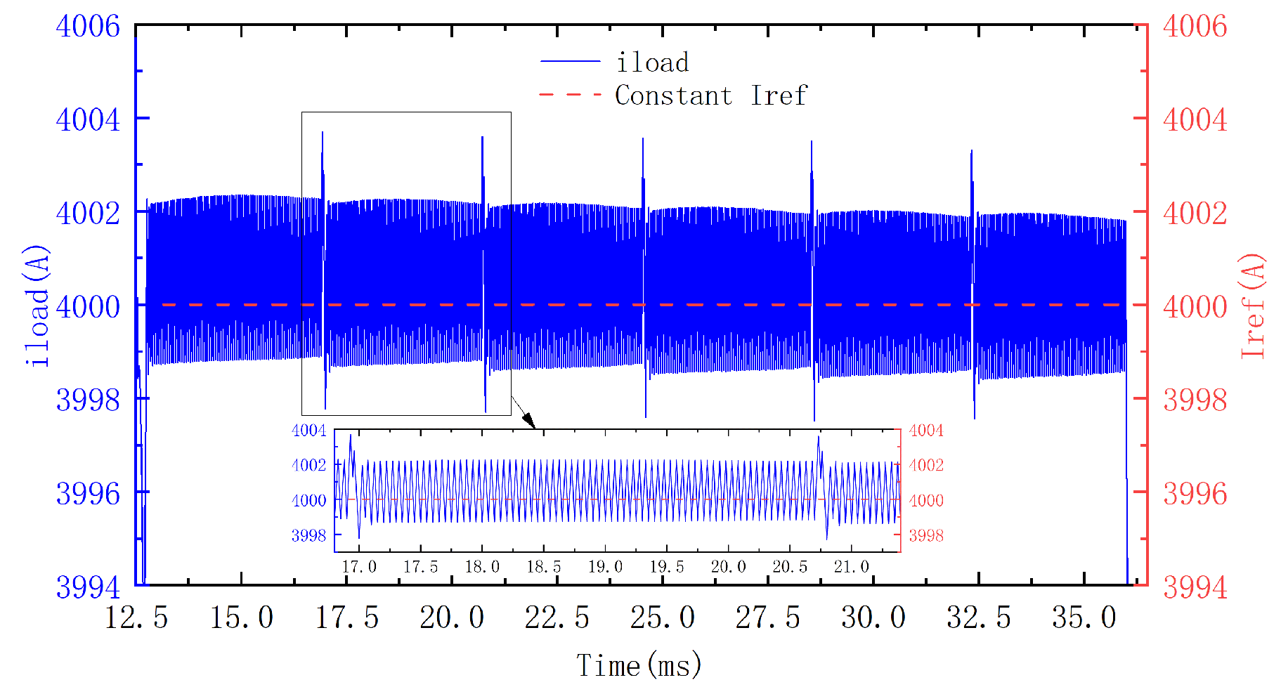
5. Experiment Results
In order to verify the correctness of the switching sequence of the capacitor bank and the feasibility of the control scheme, a prototype low-power-scale experimental platform was built, the schematic diagram of the platform is depicted in Figure 23 and the picture of it is shown in Figure 24. Experiments were carried out at a low-power scale with = 400 A and the pulse-width shortened to 16 ms.
Figure 23.
The schematic diagram of the experimental platform.
Figure 24.
The prototype low-power experimental platform.
The experimental parameters are shown in Table 5. Only voltages and currents are scaled down to a laboratory level while most of the other parameters are consistent with the designed ones. The results are shown in Figure 25, which shows the load current and currents of the main power supply structure and the ACC structure.
Table 5.
Parameters for low-power-scale experiments.
Figure 25.
Experimental waveforms of , and .
It can be seen from Figure 25 that the rising stage time and the falling stage time are within 4 ms, and the flat-top duration is more than 16 ms with four capacitors triggered sequentially, which is consistent with the simulation results.
For comparison, Figure 26 and Figure 27, respectively, illustrate the details of the load current using the conventional PI control scheme and the load current using the PI control scheme with slope compensation. Figure 26 indicates that the dynamic response speed of the traditional PI controller is insufficient. It cannot immediately stabilize the load current in response to the voltage fluctuations caused by the rapid switching of capacitors within the capacitor bank. The resulting current fluctuation range is 1.325 A, corresponding to a stability level of 3312 ppm. Figure 27 shows that after introducing slope compensation, the fluctuations caused by capacitor switching are effectively suppressed. The total current fluctuation range is reduced to 0.586 A, corresponding to a stability level of 1465 ppm. This validates the critical role of slope compensation in enhancing the stability of this current source topology.
Figure 26.
Details of using the conventional PI control scheme.
Figure 27.
Details of using the PI control scheme with slope compensation.
It has to be mentioned that the measuring system of the experiment tests has not been tuned to its best condition due to the electromagnetic interference in the environment. The currently used current transducer in the tests is very susceptible to the interference, so a digital low-pass filer along with multiple LR filters are designed to smooth the ripples of the output voltage of the current transducer, which caused the phase lag of the output current of the ACC. So, the current stability of the final tests has not reached the expected result of 1000 ppm and may be improved in later research.
6. Discussion
Regarding the electromagnetic interference (EMI) in our experimental setup, we identified the primary sources of interference as the following:
- (a).
- High-frequency switching devices, including the switches in the main circuit and components in the switching power supply on the PCB board, which generate EMI during their operation;
- (b).
- Pulse transformers on the switching driver board, contributing additional EMI;
- (c).
- Rapid magnetic field changes caused by the fast rise and fast fall of load coil currents.
These interference sources are located relatively close to the current measurement circuit, affecting waveform measurements. To address this, we plan to optimize the experimental platform’s layout in future work, aiming to increase the distance between the measurement circuit and interference sources. Additionally, we are exploring the use of a Faraday cage-style shield around the measurement circuit for further EMI mitigation.
The proposed topology addresses key challenges in high-power pulsed current systems, but several promising research avenues remain and will be considered in our future research:
- (a).
- Advanced Control Strategies: We aim to develop hybrid control architectures combining model predictive control (MPC) and AI-based ripple cancellation to achieve sub-100 ppm stability for precision applications like quantum magnetometry.
- (b).
- Wide-Bandgap Semiconductor Integration: We aim to replace silicon-based IGBTs with GaN/SiC MOSFETs to enable sub-100 ns switching and reduce switching losses, while characterizing trade-offs between device ruggedness and high di/dt capability.
- (c).
- AI-Driven Lifetime Prediction: We aim to use digital twins and federated learning to predict component lifetimes and enable proactive maintenance, addressing capacitor aging and contact erosion in high-current pulsing.
7. Conclusions
This article proposes a highly stabilized current source topology which can be applied to the 4.5 Ghz HPM plasma source as the guiding coil’s power supply. A capacitor bank is used as the main power supply which can avoid impact and harmonic pollution to the power grid and generate a fast current rising and falling stage. Thyristors are used to switch the capacitor branch of the capacitor bank and to handle most of the load current, which are much cheaper compared with IGBTs or other semiconductors of the same voltage and current level. The ACC structure which is designed to compensate for the fluctuation of the main structure uses only one high-frequency power switch S1.
The problem of the load current fluctuation caused by capacitor switching is studied and a PI control scheme utilizing slope compensation is introduced by this article to solve it. Simulation results have proved the feasibility of this control scheme. Experiments have been carried out on a prototype low-power-scale experimental platform, which realized a 400 A/16 ms/3312 ppm flat-top current with a conventional PI control scheme and a 400 A/16 ms/1465 ppm flat-top current with a PI control scheme utilizing slope compensation.
Author Contributions
Conceptualization, D.Z. and H.D.; methodology, D.Z. and Z.H.; software, D.Z.; validation, D.Z., Z.H. and W.Z.; formal analysis, D.Z.; investigation, D.Z. and Z.Z.; resources, H.D.; data curation, D.Z.; writing—original draft preparation, D.Z.; writing—review and editing, D.Z. and H.D.; writing—final version editing and confirmation—D.Z., H.D., Z.H., W.Z. and Z.Z.; visualization, D.Z.; supervision, D.Z. and H.D.; project administration, H.D.; funding acquisition, H.D. All authors have read and agreed to the published version of the manuscript.
Funding
This research was funded by the National Key Research and Development Program of China under Grant 2023YFA1607603.
Data Availability Statement
The raw data supporting the conclusions of this article will be made available by the authors on request.
Conflicts of Interest
The authors declare no conflicts of interest.
References
- Chandra, R.; Sharma, V.; Singh, S.K.; Kalyanasundaram, S.; Mitra, S.; Patel, A.; Mondal, J.; Roy, A.; Sharma, A. Design and Operation of Gigawatt Level RBWO Device for HPM Generation in S-band Frequency. In Proceedings of the 2023 First International Conference on Microwave, Antenna and Communication (MAC), Prayagraj, India, 24–26 March 2023; pp. 1–5. [Google Scholar]
- Wang, D.; Teng, Y.; Li, S.; Chen, C.; Liu, W.; Su, J.; Zhang, L.; Cheng, J.; Du, Z.; Gao, L. Pulse Lengthening of the Microwave Generated by TM02 Mode Ka-Band RBWO Operating With Low Guiding Magnetic Field. IEEE Trans. Electron Devices 2021, 68, 3015–3020. [Google Scholar] [CrossRef]
- Xiao, R.; Chen, K.; Wang, H.; Wang, D.; Shi, Y.; Gao, L. Theoretical calculation and particle-in-cell simulation of a multi-mode relativistic backward wave oscillator operating at low magnetic field. Phys. Plasmas 2022, 29, 29. [Google Scholar] [CrossRef]
- Yang, C.; Wang, H.; Meng, J.; Deng, B. The Method of Reducing the Guiding Magnetic Field of High-Band O-Type High-Power Microwave Generator. IEEE Trans. Plasma Sci. 2023, 51, 1900–1904. [Google Scholar] [CrossRef]
- Takahashi, M.; Kikuchi, S.; Inoue, N.; Sakai, N.; Murakami, M.; Yokoyama, K.; Oka, T.; Nakamura, T. NMR Relaxometry Using Outer Field of Single-Sided HTS Bulk Magnet Activated by Pulsed Field. IEEE Trans. Appl. Supercond. 2022, 32, 4602404. [Google Scholar] [CrossRef]
- Tu, P.; Ding, H.; Zhang, D.; Zhang, Z.; He, Z. A Novel Design of Multilevel Repetitive Pulse Magnetic Field System. In The Proceedings of 2023 International Conference on Wireless Power Transfer (ICWPT2023), Weihai, China, 13–15 October 2023; Springer: Singapore, 2023; Volume 1161, pp. 412–425. [Google Scholar]
- Singh, A.P.; Gopal, K.; Goswami, Y.; Kundu, M.; Varshney, P. Terahertz field generation from laser interaction with spherical nano-particles: Effect of external magnetic field. Opt. Quant. Electron. 2024, 56, 199. [Google Scholar] [CrossRef]
- Lelekhov, S.A.; Sytnikov, V.E. Conductor Design for Toroidal Field Coils of a High Magnetic Field Tokamak TRT20. IEEE Trans. Appl. Supercond. 2022, 24, 4201805. [Google Scholar] [CrossRef]
- Grössinger, R.; Schönhart, M.; Kriegisch, M.; Haas, M.; Sassik, H. High Field Facilities at TU Vienna. J. Low Temp. Phys. 2010, 159, 394–401. [Google Scholar] [CrossRef]
- Ding, H.; Hu, J.; Liu, W.; Xu, Y.; Jiang, C.; Ding, T. Design of a 135 MW Power Supply for a 50 T Pulsed Magnet. IEEE Trans. Appl. Supercond. 2012, 22, 5400504. [Google Scholar] [CrossRef]
- Zhang, S.; Wang, Z.; Ding, T.; Xiao, H.; Xie, J.; Han, X. Realization of High-Stability Flat-Top Pulsed Magnetic Fields by a Bypass Circuit of IGBTs in the Active Region. IEEE Trans. Power Electron. 2020, 35, 2436–2444. [Google Scholar] [CrossRef]
- Ling, P.E.W.; Mao, A.; Guan, J.; Ma, X.; Li, H.; Yu, Z.; Ding, M. A Pulsed Power Supply Based on an Optimized SFPFN Scheme Producing Large Currents With a Flat Top on a Heavily Inductive Load. IEEE Trans. Power Electron. 2021, 36, 11221–11233. [Google Scholar]
- Zhou, Y.; Huang, J.; Wang, S.; Jiang, W.; Chen, J. Principle of designing slope compensation in PFC Boost converter. Sci. China Ser. F Inf. Sci. 2009, 52, 2226–2233. [Google Scholar] [CrossRef]
- Aroudi, A.E.; Mandal, K.; Al-Numay, M.S.; Giaouris, D.; Banerjee, S. Piecewise Quadratic Slope Compensation Technique for DC-DC Switching Converters. IEEE Trans. Circuits Syst. I Regul. Pap. 2020, 67, 5574–5585. [Google Scholar] [CrossRef]
Disclaimer/Publisher’s Note: The statements, opinions and data contained in all publications are solely those of the individual author(s) and contributor(s) and not of MDPI and/or the editor(s). MDPI and/or the editor(s) disclaim responsibility for any injury to people or property resulting from any ideas, methods, instructions or products referred to in the content. |
© 2025 by the authors. Licensee MDPI, Basel, Switzerland. This article is an open access article distributed under the terms and conditions of the Creative Commons Attribution (CC BY) license (https://creativecommons.org/licenses/by/4.0/).