
REO: Revisiting Erase Operation for Improving Lifetime and Performance of Modern NAND Flash-Based SSDs †


Abstract
1. Introduction
- We introduce REO, a new block erasure mechanism that dynamically adjusts the erase latency and voltage based on varying erase characteristics of the target flash blocks.
- We validate the feasibility and reliability of REO via extensive characterization of real 3D NAND flash chips.
2. Background
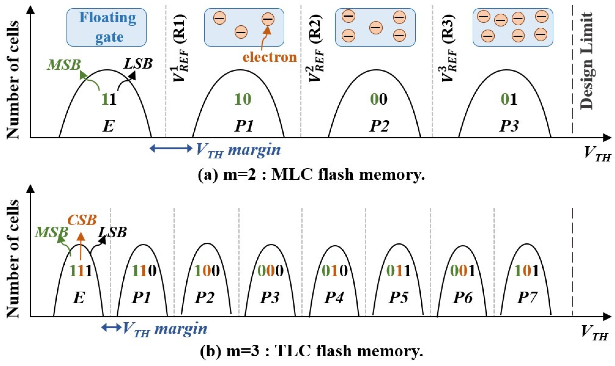
2.1. NAND Flash Basics
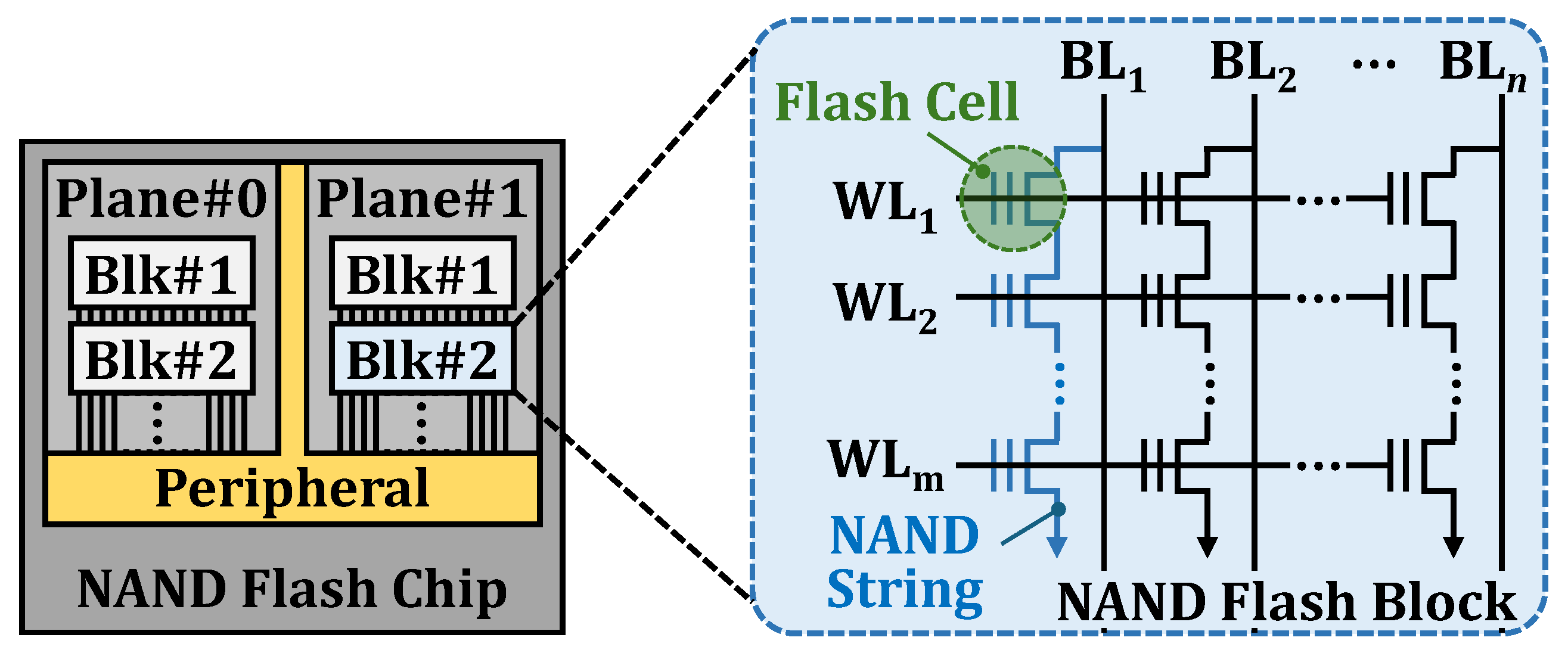
2.2. Organizational Basics of 3D Vertical NAND Flash Memory
2.3. The 3D NAND Manufacturing Process
2.4. NAND Flash Reliability
2.5. VREF Adjustment Techniques to Handle Read Errors: Read-Retries
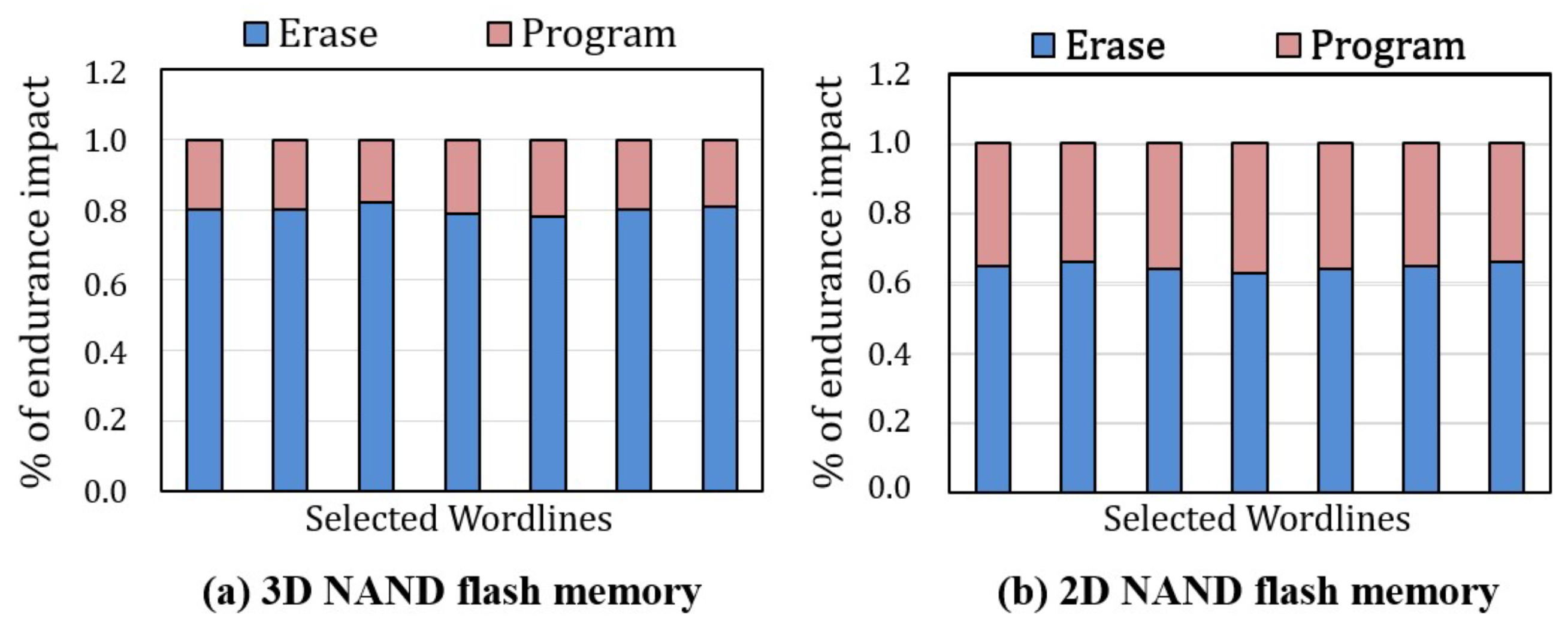
2.6. Negative Impact of Erase Operation on I/O Performance
3. Motivation
3.1. Negative Impact of Erase Operations
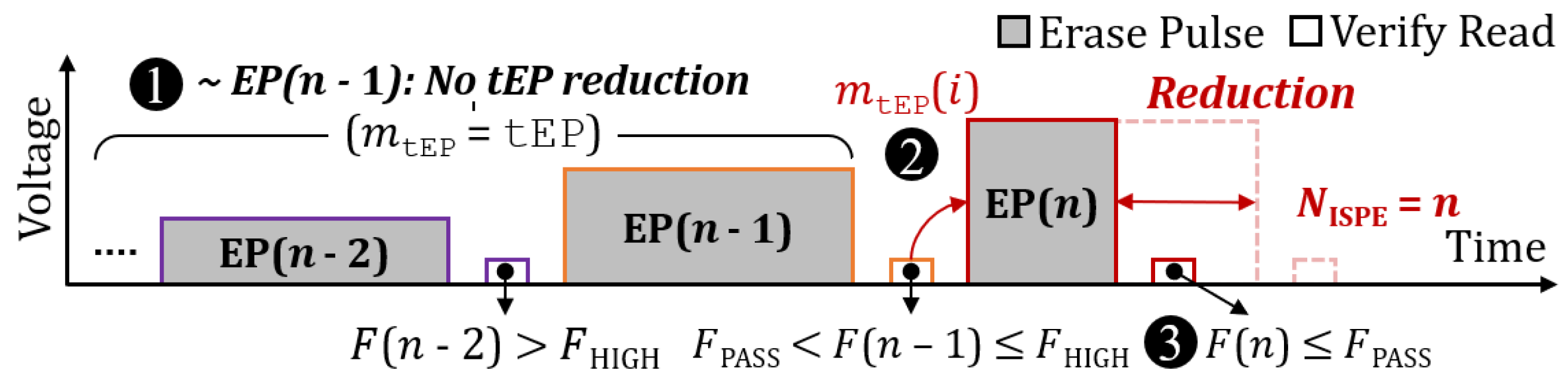
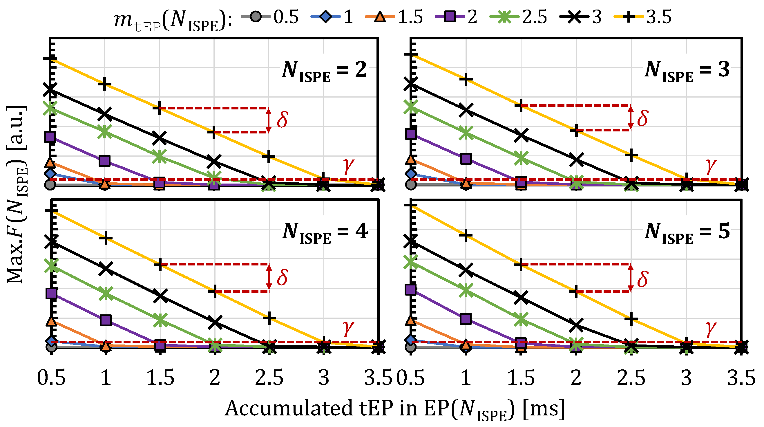
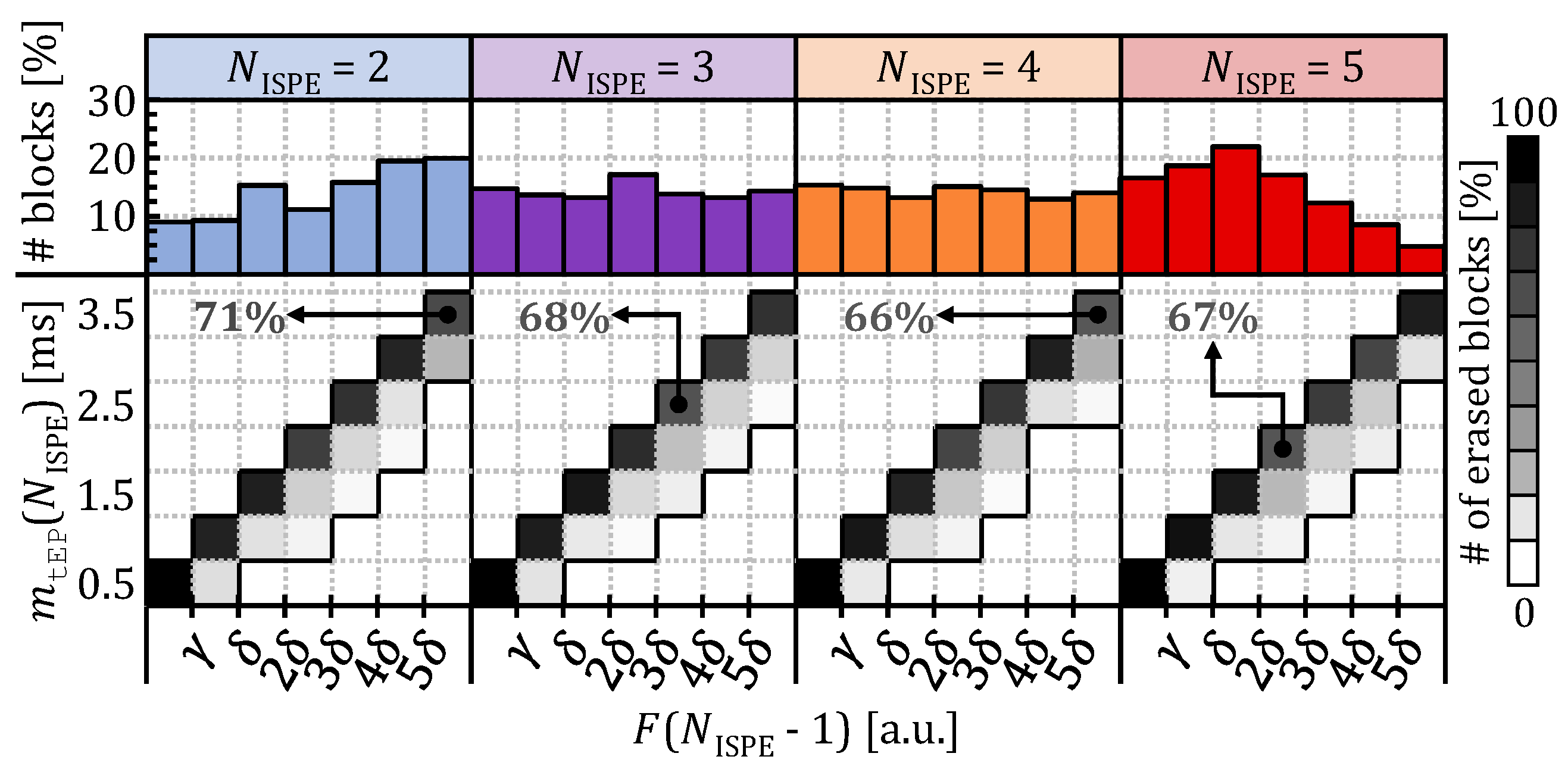
3.2. Incremental Step Pulse Erasure (ISPE) and Its Limitations
3.3. Per-WL Erase Speed Variability
3.4. Limitations of the State of the Art
4. REO: Revisiting Erase Operation
5. Device Characterization Study
5.1. Characterization Methodology
5.2. Fail-Bit Count vs. Near-Optimal Erase Latency
5.3. Reliability Margin for Aggressive tEP Reduction
5.4. WL Gate Voltage vs. Erase Speed
5.5. Applicability of REO for Other Types of Chips
6. Design and Implementation
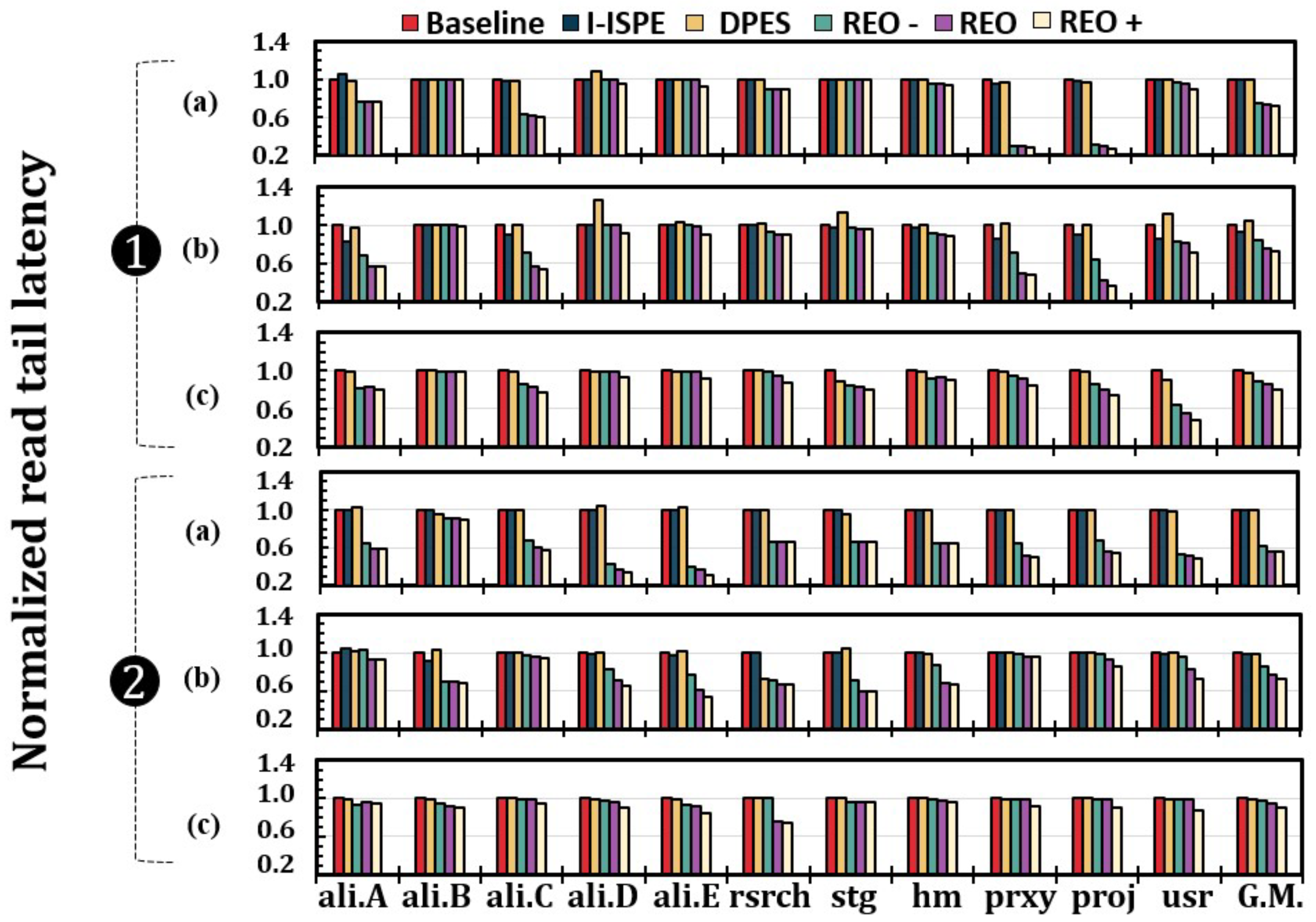
7. Evaluation
7.1. Evaluation Methodology
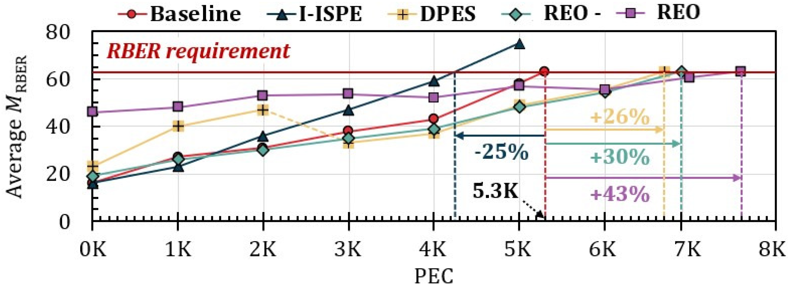
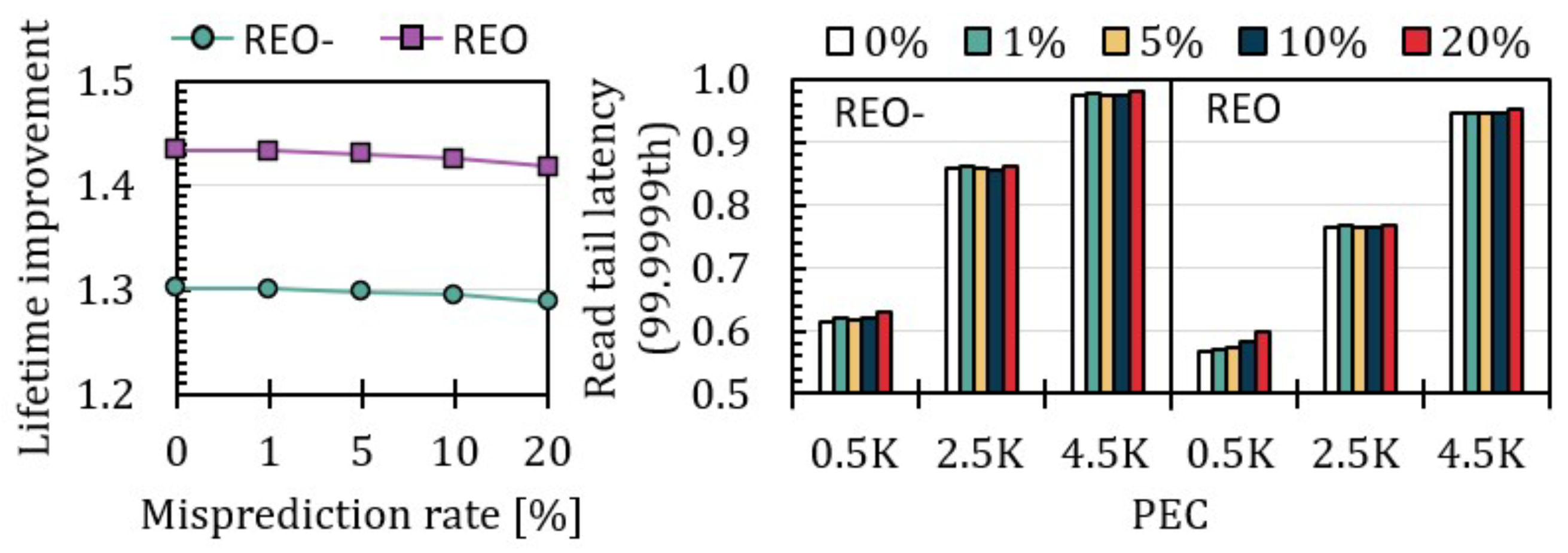
7.2. Impact on SSD Lifetime
7.3. Impact on I/O Performance
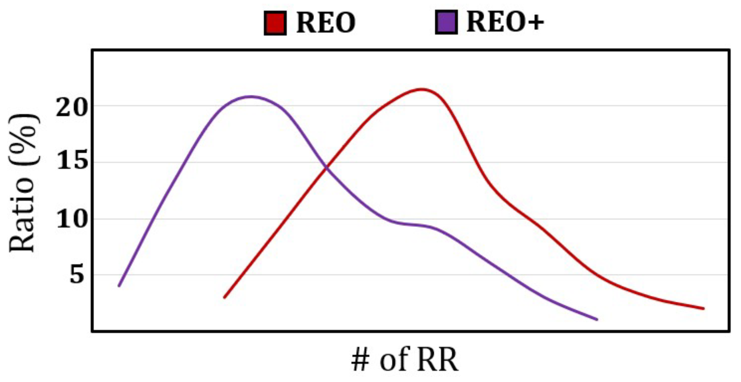
7.4. Sensitivity Analysis
8. Related Work
9. Conclusions
Author Contributions
Funding
Data Availability Statement
Conflicts of Interest
Appendix A. Terminology Summary

| Terminology | Definition |
|---|---|
| NISPE | Number of erase loops for complete erasure |
| VR(i)/EP(i) | i-th Verify-Read/Erase-Pulse step |
| F(i) | Number of fail bits after EP(i) |
| FPASS | Predefined erase pass threshold |
| FHIGH | Full erase pulse threshold |
| tEP/tVR | Erase-Pulse/Verify-Read latency |
| VWG | WL Gate Voltage |
| mtBERS/mtEP(i) | Minimum tBERS/tEP(i) |
| MRBER | Maximum raw bit errors |
References
- Samsung. Samsung Enterprise SSDs. 2023. Available online: https://semiconductor.samsung.com/ssd/enterprise-ssd (accessed on 9 February 2025).
- SK Hynix. SK Hynix Enterprise SSDs. 2023. Available online: https://product.skhynix.com/products/ssd/essd.go (accessed on 9 February 2025).
- Micron. Micron Enterprise SSDs. 2023. Available online: https://www.micron.com/products/ssd/product-lines/9400 (accessed on 9 February 2025).
- Western Digital. Western Digital Data Center SSDs. 2023. Available online: https://github.com/axboe/fio (accessed on 9 February 2025).
- Wong, H.S.P.; Raoux, S.; Kim, S.; Liang, J.; Reifenberg, J.P.; Rajendran, B.; Asheghi, M.; Goodson, K.E. Phase Change Memory. Proc. IEEE 2010, 98, 2201–2227. [Google Scholar] [CrossRef]
- Zangeneh, M.; Joshi, A. Design and Optimization of Nonvolatile Multibit 1T1R Resistive RAM. IEEE Trans. Very Large Scale Integr. (VLSI) Syst. 2013, 22, 1815–1828. [Google Scholar] [CrossRef]
- Aggarwal, S. STT–MRAM: High Density Persistent Memory Solution. Available online: https://www.flashmemorysummit.com/Proceedings2019/08-07-Wednesday/20190807_NEWM-202B-1_Aggarwal.pdf (accessed on 9 February 2025).
- Kawashima, S.; Cross, J.S. FeRAM; Springer: New York, NY, USA, 2009. [Google Scholar]
- Cho, J.; Kang, D.C.; Park, J.; Nam, S.W.; Song, J.H.; Jung, B.K.; Lyu, J.; Lee, H.; Kim, W.-T.; Jeon, H.; et al. 30.3 A 512Gb 3b/Cell 7 th-Generation 3D-NAND Flash Memory with 184MB/sWrite Throughput and 2.0 Gb/s Interface. In Proceedings of the 2021 IEEE International Solid-State Circuits Conference (ISSCC), San Francisco, CA, USA, 13–22 February 2021. [Google Scholar]
- Kim, M.; Yun, S.W.; Park, J.; Park, H.K.; Lee, J.; Kim, Y.S.; Na, D.; Choi, S.; Song, Y.; Lee, J.; et al. A 1Tb 3b/Cell 8th-Generation 3D-NAND Flash Memory with 164MB/s Write Throughput and a 2.4Gb/s Interface. In Proceedings of the 2022 IEEE International Solid-State Circuits Conference (ISSCC), San Francisco, CA, USA, 20–26 February 2022. [Google Scholar]
- Hong, D.; Kim, M.; Cho, G.; Lee, D.; Kim, J. GuardedErase: Extending SSD Lifetimes by Protecting Weak Wordlines. In Proceedings of the 20th USENIX Conference on File and Storage Technologies (FAST), Santa Clara, CA, USA, 22–24 February 2022. [Google Scholar]
- Wu, G.; He, X. Reducing SSD Read Latency via NAND Flash Program and Erase Suspension. In Proceedings of the 10th USENIX Conference on File and Storage Technologies (FAST), San Jose, CA, USA, 15–17 February 2012. [Google Scholar]
- Kim, S.; Bae, J.; Jang, H.; Jin, W.; Gong, J.; Lee, S.; Ham, T.J.; Lee, J.W. Practical Erase Suspension for Modern Low-latency SSDs. In Proceedings of the 2019 USENIX Annual Technical Conference (ATC), Renton, WA, USA, 10–12 July 2019. [Google Scholar]
- Cai, Y.; Ghose, S.; Haratsch, E.F.; Luo, Y.; Mutlu, O. Error Characterization, Mitigation, and Recovery in Flash-Memory-Based Solid-State Drives. Proc. IEEE 2017, 105, 1666–1704. [Google Scholar] [CrossRef]
- Kim, M.; Chun, M.; Hong, D.; Kim, Y.; Cho, G.; Lee, D.; Kim, J. RealWear: Improving performance and lifetime of SSDs using a NAND aging marker. Perform. Eval. 2021, 48, 120–121. [Google Scholar] [CrossRef]
- Lee, D.W.; Cho, S.; Kang, B.W.; Park, S.; Park, B.; Cho, M.K.; Ahn, K.O.; Yang, Y.S.; Park, S.W. The Operation Algorithm for Improving the Reliability of TLC (Triple Level Cell) NAND Flash Characteristics. In Proceedings of the 2011 3rd IEEE International Memory Workshop (IMW), Monterey, CA, USA, 22–25 May 2011. [Google Scholar]
- Lee, J.; Kim, Y.; Shipman, G.M.; Oral, S.; Wang, F.; Kim, J. A Semi-Preemptive Garbage Collector for Solid State Drives. In Proceedings of the IEEE International Symposium on Performance Analysis of Systems and Software (ISPASS), Austin, TX, USA, 10–12 April 2011. [Google Scholar]
- Cui, J.; Zhang, Y.; Huang, J.; Wu, W.; Yang, J. ShadowGC: Cooperative Garbage Collection with Multi-level Buffer for Performance Improvement in NAND flash-based SSDs. In Proceedings of the 2018 Design, Automation & Test in Europe Conference & Exhibition (DATE), Dresden, Germany, 19–23 March 2018. [Google Scholar]
- Kang, W.; Yoo, S. Dynamic Management of Key States for Reinforcement Learning-Assisted Garbage Collection to Reduce Long Tail Latency in SSD. In Proceedings of the 55th Annual Design Automation Conference (DAC), San Francisco, CA, USA, 24–29 June 2018. [Google Scholar]
- Shahidi, N.; Kandemir, M.T.; Arjomand, M.; Das, C.R.; Jung, M.; Sivasubramaniam, A. Exploring the Potentials of Parallel Garbage Collection in SSDs for Enterprise Storage Systems. In Proceedings of the International Conference for High Performance Computing, Networking, Storage and Analysis (SC), Salt Lake City, UT, USA, 13–18 November 2016. [Google Scholar]
- Choi, W.; Jung, M.; Kandemir, M.; Das, C. Parallelizing Garbage Collection with I/O to Improve Flash Resource Utilization. In Proceedings of the 27th International Symposium on High-Performance Parallel and Distributed Computing (HPDC), Tempe, AZ, USA, 11–15 June 2018. [Google Scholar]
- Guo, J.; Hu, Y.; Mao, B.; Wu, S. Parallelism and Garbage Collection Aware I/O Scheduler with Improved SSD Performance. In Proceedings of the 2017 IEEE International Parallel and Distributed Processing Symposium (IPDPS), Orlando, FL, USA, 19 May–2 June 2017. [Google Scholar]
- Kang, W.; Shin, D.; Yoo, S. Reinforcement Learning-Assisted Garbage Collection to Mitigate Long-Tail Latency in SSD. ACM Trans. Embed. Comput. Syst. (TECS) 2017, 16, 1–20. [Google Scholar] [CrossRef]
- Yang, P.; Xue, N.; Zhang, Y.; Zhou, Y.; Sun, L.; Chen, W.; Chen, Z.; Xia, W.; Li, J.; Kwon, K. Reducing Garbage Collection Overhead in SSD Based on Workload Prediction. In Proceedings of the 11th USENIX Workshop on Hot Topics in Storage and File Systems (HotStorage), Renton, WA, USA, 8–9 July 2019. [Google Scholar]
- Lee, J.; Kim, Y.; Shipman, G.M.; Oral, S.; Kim, J. Preemptible I/O Scheduling of Garbage Collection for Solid State Drives. IEEE Trans. Comput. Aided Des. Integr. Circuits Syst. (TCAD) 2013, 32, 247–260. [Google Scholar] [CrossRef]
- Murugan, M.; Du, D. Rejuvenator: A Static Wear Leveling Algorithm for NAND Flash Memory with Minimized Overhead. In Proceedings of the 2011 IEEE 27th Symposium on Mass Storage Systems and Technologies (MSST), Denver, CO, USA, 23–27 May 2011. [Google Scholar]
- Li, J.; Xu, X.; Peng, X.; Liao, J. Pattern-based Write Scheduling and Read Balance-oriented Wear-Leveling for Solid State Drivers. In Proceedings of the 2019 35th Symposium on Mass Storage Systems and Technologies (MSST), Santa Clara, CA, USA, 20–24 May 2019. [Google Scholar]
- Dharamjeet; Chen, Y.S.; Chen, T.Y.; Kuan, Y.H.; Chang, Y.H. LLSM: A Lifetime-Aware Wear-Leveling for LSM-Tree on NAND Flash Memory. IEEE Trans. Comput. Aided Des. Integr. Circuits Syst. (TCAD) 2022, 41, 3946–3956. [Google Scholar] [CrossRef]
- Jeong, J.; Hahn, S.S.; Lee, S.; Kim, J. Improving NAND Endurance by Dynamic Program and Erase Scaling. In Proceedings of the 5th USENIX Workshop on Hot Topics in Storage and File Systems (HotStorage), San Jose, CA, USA, 27–28 June 2013. [Google Scholar]
- Jeong, J.; Hahn, S.S.; Lee, S.; Kim, J. Lifetime Improvement of NAND Flash-based Storage Systems Using Dynamic Program and Erase Scaling. In Proceedings of the 12th USENIX Conference on File and Storage Technologies (FAST), Santa Clara, CA, USA; 2014. [Google Scholar]
- Jeong, J.; Youngsun, S.; Hahn, S.S.; Lee, S.; Kim, J. Dynamic Erase Voltage and Time Scaling for Extending Lifetime of NAND Flash-Based SSDs. IEEE Trans. Comput. (TC) 2017, 66, 616–630. [Google Scholar] [CrossRef]
- Shim, Y.; Kim, M.; Chun, M.; Park, J.; Kim, Y.; Kim, J. Exploiting Process Similarity of 3D Flash Memory for High Performance SSDs. In Proceedings of the 52nd Annual IEEE/ACM International Symposium on Microarchitecture (MICRO), Columbus, OH, USA, 12–16 October 2019. [Google Scholar]
- Luo, Y.; Ghose, S.; Cai, Y.; Haratsch, E.F.; Mutlu, O. Improving 3D NAND Flash Memory Lifetime by Tolerating Early Retention Loss and Process Variation. Proc. ACM Meas. Anal. Comput. Syst. (POMACS) 2018, 2, 1–48. [Google Scholar] [CrossRef]
- Wang, Y.; Dong, L.; Mao, R. P-Alloc: Process-Variation Tolerant Reliability Management for 3D Charge-Trapping Flash Memory. ACM Trans. Embed. Comput. Syst. (TECS) 2017, 16, 1–19. [Google Scholar] [CrossRef]
- Chen, S.H.; Chen, Y.T.; Wei, H.W.; Shih, W.K. Boosting the Performance of 3D Charge Trap NAND Flash with Asymmetric Feature Process Size Characteristic. In Proceedings of the 2017 54th ACM/EDAC/IEEE Design Automation Conference (DAC), San Francisco, CA, USA, 18–22 June 2017. [Google Scholar]
- Hung, C.H.; Chang, M.F.; Yang, Y.S.; Kuo, Y.J.; Lai, T.N.; Shen, S.J.; Hsu, J.Y.; Hung, S.N.; Lue, H.T.; Shih, Y.H.; et al. Layer-Aware Program-and-Read Schemes for 3D Stackable Vertical-Gate BE-SONOS NAND Flash Against Cross-Layer Process Variations. IEEE J. Solid-State Circuits (JSSC) 2015, 50, 1491–1501. [Google Scholar] [CrossRef]
- Yen, J.N.; Hsieh, Y.C.; Chen, C.Y.; Chen, T.Y.; Yang, C.L.; Cheng, H.Y.; Luo, Y. Efficient Bad Block Management with Cluster Similarity. In Proceedings of the 2022 IEEE International Symposium on High-Performance Computer Architecture (HPCA), Seoul, Republic of Korea, 2–6 April 2022. [Google Scholar]
- Li, Q.; Ye, M.; Cui, Y.; Shi, L.; Li, X.; Kuo, T.W.; Xue, C.J. Shaving Retries with Sentinels for Fast Read over High-Density 3D Flash. In Proceedings of the 2020 53rd Annual IEEE/ACM International Symposium on Microarchitecture (MICRO), Athens, Greece, 17–21 October 2020. [Google Scholar]
- Cai, Y.; Haratsch, E.F.; Mutlu, O.; Mai, K. Threshold Voltage Distribution in MLC NAND Flash Memory: Characterization, Analysis, and Modeling. In Proceedings of the 2013 Design, Automation & Test in Europe Conference & Exhibition (DATE), Grenoble, France, 18–22 March 2013. [Google Scholar]
- Cai, Y.; Luo, Y.; Ghose, S.; Mutlu, O. Read Disturb Errors in MLC NAND Flash Memory: Characterization, Mitigation, and Recovery. In Proceedings of the 45th Annual IEEE/IFIP International Conference on Dependable Systems and Networks (DSN), Rio de Janeiro, Brazil, 22–25 June 2015. [Google Scholar]
- Park, J.; Kim, M.; Chun, M.; Orosa, L.; Kim, J.; Mutlu, O. Reducing Solid-State Drive Read Latency by Optimizing Read-Retry. In Proceedings of the 26th ACM International Conference on Architectural Support for Programming Languages and Operating Systems (ASPLOS), Virtual, 19–23 April 2021. [Google Scholar]
- Tavakkol, A.; Gómez-Luna, J.; Sadrosadati, M.; Ghose, S.; Mutlu, O. MQSim: A Framework for Enabling Realistic Studies of Modern Multi-Queue SSD Devices. In Proceedings of the 16th USENIX Conference on File and Storage Technologies (FAST), Oakland, CA, USA, 12–15 February 2018. [Google Scholar]
- Maserjian, J.; Zamani, N. Behavior of the Si/SiO2 interface observed by Fowler-Nordheim tunneling. J. Appl. Phys. 1982, 53, 559–567. [Google Scholar] [CrossRef]
- Park, J.; Azizi, R.; Oliveira, G.F.; Sadrosadati, M.; Nadig, R.; Novo, D.; Gómez-Luna, J.; Kim, M.; Mutlu, O. Flash-Cosmos: In-Flash Bulk Bitwise Operations Using Inherent Computation Capability of NAND Flash Memory. In Proceedings of the 2022 55th IEEE/ACM International Symposium on Microarchitecture (MICRO), Chicago, IL, USA, 1–10 October 2022. [Google Scholar]
- Choi, J.; Seol, K.S. 3D approaches for non-volatile memory. In Proceedings of the Symposium on VLSI Technology-Digest of Technical Papers, Kyoto, Japan, 15–17 June 2011. [Google Scholar]
- Park, Y.; Lee, J.; Cho, S.S.; Jin, G.; Jung, E. Scaling and reliability of NAND flash devices. In Proceedings of the IEEE International Reliability Physics Symposium (IRPS), Monterey, CA, USA, 14–18 April 2014. [Google Scholar]
- Jang, J.; Kim, H.S.; Cho, W.; Cho, H.; Kim, J.; Shim, S.I.; Younggoan; Jeong, J.H.; Son, B.K.; Kim, D.W.; et al. Vertical cell array using TCAT(Terabit Cell Array Transistor) technology for ultra high density NAND flash memory. In Proceedings of the 2009 Symposium on VLSI Technology, Kyoto, Japan, 16–18 June 2009. [Google Scholar]
- Ha, K.; Jeong, J.; Kim, J. An Integrated Approach for Managing Read Disturbs in High-Density NAND Flash Memory. IEEE Trans. Comput. Aided Des. Integr. Circuits Syst. (TCAD) 2016, 35, 1079–1091. [Google Scholar] [CrossRef]
- Liu, C.Y.; Lee, Y.; Jung, M.; Kandemir, M.T.; Choi, W. Prolonging 3D NAND SSD Lifetime via Read Latency Relaxation. In Proceedings of the 26th ACM International Conference on Architectural Support for Programming Languages and Operating Systems (ASPLOS), 12–23 April 2021. [Google Scholar]
- Cai, Y.; Mutlu, O.; Haratsch, E.F.; Mai, K. Program Interference in MLC NAND Flash Memory: Characterization, Modeling, and Mitigation. In Proceedings of the IEEE 31st International Conference on Computer Design (ICCD), Asheville, NC, USA, 6–9 October 2013. [Google Scholar]
- Park, J.; Jeong, J.; Lee, S.; Song, Y.; Kim, J. Improving Performance and Lifetime of NAND Storage Systems Using Relaxed Program Sequence. In Proceedings of the 53nd ACM/EDAC/IEEE Design Automation Conference (DAC), Austin, TX, USA, 5–9 June 2016. [Google Scholar]
- Kim, M.; Lee, J.; Lee, S.; Park, J.; Kim, J. Improving Performance and Lifetime of Large-page NAND Storages Using Erase-Free Subpage Programming. In Proceedings of the 54th ACM/EDAC/IEEE Design Automation Conference (DAC), San Francisco, USA, 18–22 June 2017. [Google Scholar]
- Cai, Y.; Ghose, S.; Luo, Y.; Mai, K.; Mutlu, O.; Haratsch, E.F. Vulnerabilities in MLC NAND Flash Memory Programming: Experimental Analysis, Exploits, and Mitigation Techniques. In Proceedings of the IEEE International Symposium on High Performance Computer Architecture (HPCA), Austin, TX, USA, 4–8 February 2017. [Google Scholar]
- Gallager, R. Low-Density Parity-Check Codes. IRE Trans. Inf. Theory 1962, 8, 21–28. [Google Scholar] [CrossRef]
- Micheloni, R.; Marelli, A.; Eshghi, K. Inside Solid State Drives (SSDs); Springer: Berlin, Germany, 2012. [Google Scholar]
- Yan, S.; Li, H.; Hao, M.; Tong, M.H.; Sundararaman, S.; Chien, A.A.; Gunawi, H.S. Tiny-Tail Flash: Near-Perfect Elimination of Garbage Collection Tail Latencies in NAND SSDs. ACM Trans. Storage 2017, 13, 1–26. [Google Scholar] [CrossRef]
- Schuegraf, K.; Hu, C. Effects of temperature and defects on breakdown lifetime of thin SiO/sub 2/at very low voltages. In Proceedings of the IEEE International Reliability Physics Symposium (IRPS), San Jose, CA, USA, 11–14 April 1994. [Google Scholar]
- Yuh, J.; Li, J.; Li, H.; Oyama, Y.; Hsu, C.; Anantula, P.; Jeong, S.; Amarnath, A.; Darne, S.; Bhatia, S.; et al. A 1-Tb 4b/Cell 4-Plane 162-Layer 3D Flash Memory With a 2.4-Gb/s I/O Speed Interface. In Proceedings of the 2022 IEEE International Solid-State Circuits Conference (ISSCC), San Francisco, CA, USA, 20–26 February 2022. [Google Scholar]
- Kim, B.; Lee, S.; Hah, B.; Park, K.; Park, Y.; Jo, K.; Noh, Y.; Seol, H.; Lee, H.; Shin, J.; et al. 28.2 A High-Performance 1Tb 3b/Cell 3D-NAND Flash with a 194MB/s Write Throughput on over 300 Layers i. In Proceedings of the 2023 IEEE International Solid- State Circuits Conference (ISSCC), San Francisco, CA, USA, 19–23 February 2023. [Google Scholar]
- Micheloni, R.; Crippa, L.; Marelli, A. Inside NAND Flash Memories; Springer: Berlin, Germany, 2010. [Google Scholar]
- Hollmer, S.C.; Hu, C.Y.; Le, B.Q.; Chen, P.L.; Su, J.; Gutala, R.; Bill, C. Erase Verify Scheme for NAND Flash. US Patent 6,009,014, 28 December 1999. [Google Scholar]
- Aritome, S. NAND Flash Memory Technologies; Wiley & Sons: Hoboken, NJ, USA, 2015. [Google Scholar]
- Ito, T.; Taito, Y. SONOS Split-Gate eFlash Memory. In Embedded Flash Memory for Embedded Systems: Technology, Design for Sub-Systems, and Innovations; Springer: Berlin, Germany, 2018. [Google Scholar]
- Chen, S.H.; Chang, Y.H.; Liang, Y.P.; Wei, H.W.; Shih, W.K. An Erase Efficiency Boosting Strategy for 3D Charge Trap NAND Flash. IEEE Trans. Comput. (TC) 2018, 67, 1246–1258. [Google Scholar] [CrossRef]
- Lue, H.T.; Hsu, T.H.; Wu, C.J.; Chen, W.C.; Yeh, T.H.; Chang, K.P.; Hsieh, C.C.; Du, P.Y.; Hsiao, Y.H.; Jiang, Y.W.; et al. A Novel Double-density, Single-Gate Vertical Channel (SGVC) 3D NAND Flash That Is Tolerant to Deep Vertical Etching CD Variation and Possesses Robust Read-disturb Immunity. In Proceedings of the 2015 IEEE International Electron Devices Meeting (IEDM), San Francisco, CA, USA, 7–9 December 2015. [Google Scholar]
- Cha, J.; Kang, S. Data Randomization Scheme for Endurance Enhancement and Interference Mitigation of Multilevel Flash Memory Devices. Etri J. 2013, 35, 166–169. [Google Scholar] [CrossRef]
- Favalli, M.; Zambelli, C.; Marelli, A.; Micheloni, R.; Olivo, P. A Scalable Bidimensional Randomization Scheme for TLC 3D NAND Flash Memories. Micromachines 2021, 12, 759. [Google Scholar] [CrossRef]
- ONFI Workgroup. Open NAND Flash Interface Specification 4.1. Available online: https://onfi.org/files/onfi_4_1_gold.pdf (accessed on 9 February 2025).
- Kang, D.; Jeong, W.; Kim, C.; Kim, D.H.; Cho, Y.S.; Kang, K.T.; Ryu, J.; Kang, K.M.; Lee, S.; Kim, W.; et al. 256Gb 3b/cell V-NAND Flash Memory with 48 Stacked WL Layers. In Proceedings of the 2016 IEEE International Solid-State Circuits Conference (ISSCC), San Francisco, CA, USA, 31 January–4 February 2016. [Google Scholar]
- JEDEC. JESD218B.02: Solid-State Drive (SSD) Requirements and Endurance Test Method. 2022. Available online: https://www.jedec.org/standards-documents/docs/jesd218b01 (accessed on 9 February 2025).
- Arrhenius, S. Über die Dissociationswärme und den Einfluss der Temperatur auf den Dissociationsgrad der Elektrolyte. Z. Phys. Chem. 1889, 4, 96–116. [Google Scholar] [CrossRef]
- Micheloni, R. 3D Flash Memories; Springer: Berlin, Germany, 2016. [Google Scholar]
- Vättö, K. Samsung SSD 840: Testing the Endurance of TLC NAND. 2012. Available online: https://www.anandtech.com/show/6459/samsung-ssd-840-testing-the-endurance-of-tlc-nand (accessed on 9 February 2025).
- Tallis, B. The Samsung 960 Pro (2TB) SSD Review. 2016. Available online: https://www.anandtech.com/show/10754/samsung-960-pro-ssd-review (accessed on 9 February 2025).
- Gupta, A.; Kim, Y.; Urgaonkar, B. DFTL: A Flash Translation Layer Employing Demand-Based Selective Caching of Page-Level Address Mappings. In Proceedings of the 14th International Conference on Architectural Support for Programming Languages and Operating Systems (ASPLOS), Washington, DC, USA, 7–11 March 2009. [Google Scholar]
- Weisberg, P.; Wiseman, Y. Using 4KB page size for Virtual Memory is obsolete. In Proceedings of the 2009 IEEE International Conference on Information Reuse & Integration, Las Vegas, NV, USA, 10–12 August 2009. [Google Scholar]
- Chang, L.P.; Kuo, T.W. An Adaptive Striping Architecture for Flash Memory Storage Systems of Embedded Systems. In Proceedings of the Eighth IEEE Real-Time and Embedded Technology and Applications Symposium (RTAS), San Jose, CA, USA, 27 September 2002. [Google Scholar]
- Li, J.; Wang, Q.; Lee, P.P.C.; Shi, C. An In-Depth Analysis of Cloud Block Storage Workloads in Large-Scale Production. In Proceedings of the 2020 IEEE International Symposium on Workload Characterization (IISWC), Beijing, China, 27–30 October 2020. [Google Scholar]
- Narayanan, D.; Donnelly, A.; Rowstron, A. Write Off-Loading: Practical Power Management for Enterprise Storage. ACM Trans. Storage (TOS) 2008, 4, 1–23. [Google Scholar] [CrossRef]
- Nadig, R.; Sadrosadati, M.; Mao, H.; Ghiasi, N.M.; Tavakkol, A.; Park, J.; Sarbazi-Azad, H.; Luna, J.G.; Mutlu, O. Venice: Improving Solid-State Drive Parallelism at Low Cost via Conflict-Free Accesses. In Proceedings of the 50th Annual International Symposium on Computer Architecture (ISCA), Orlando, FL, USA, 17–21 June 2023. [Google Scholar]
- Liu, R.; Tan, Z.; Long, L.; Wu, Y.; Tan, Y.; Liu, D. Improving Fairness for SSD Devices through DRAM Over-Provisioning Cache Management. IEEE Trans. Parallel Distrib. Syst. (TPDS) 2022, 33, 2444–2454. [Google Scholar] [CrossRef]
- Liu, R.; Liu, D.; Chen, X.; Tan, Y.; Zhang, R.; Liang, L. Self-Adapting Channel Allocation for Multiple Tenants Sharing SSD Devices. IEEE Trans. Comput. Aided Des. Integr. Circuits Syst. (TCAD) 2022, 41, 294–305. [Google Scholar] [CrossRef]
- Lv, Y.; Shi, L.; Song, Y.; Xue, C.J. Access Characteristic Guided Partition for NAND Flash based High-Density SSDs. IEEE Trans. Comput. Aided Des. Integr. Circuits Syst. (TCAD) 2023, 42, 4643–4656. [Google Scholar] [CrossRef]
- Wu, J.; Li, J.; Sha, Z.; Cai, Z.; Liao, J. Adaptive Switch on Wear Leveling for Enhancing I/O Latency and Lifetime of High-Density SSDs. IEEE Trans. Comput. Aided Des. Integr. Circuits Syst. (TCAD) 2022, 41, 4040–4051. [Google Scholar] [CrossRef]
- DeCandia, G.; Hastorun, D.; Jampani, M.; Kakulapati, G.; Lakshman, A.; Pilchin, A.; Sivasubramanian, S.; Vosshall, P.; Vogels, W. Dynamo: Amazon’s Highly Available Key-Value Store. In Proceedings of the Twenty-First ACM SIGOPS Symposium on Operating Systems Principles (SOSP), Stevenson, WA, USA, 14–17 October 2007. [Google Scholar]
- Gunawi, H.S.; Hao, M.; Suminto, R.O.; Laksono, A.; Satria, A.D.; Adityatama, J.; Eliazar, K.J. Why Does the Cloud Stop Computing? Lessons from Hundreds of Service Outages. In Proceedings of the Seventh ACM Symposium on Cloud Computing (SoCC), Santa Clara, CA, USA, 5–7 October 2016. [Google Scholar]


| NISPE | F(NISPE − 1) | |||||||
| ≤2 | ≤3 | ≤4 | ≤5 | ≤6 | ≤7 | |||
| 1 | 0.5/0 | 1/0 | 1.5/0.5 | 2/1 | 2.5/1.5 | 2.5/2 | 2.5/2.5 | 2.5/2.5 |
| 2 | 0.5/0 | 1/0 | 1.5/0.5 | 2/1 | 2.5/1.5 | 3/2 | 3.5/2.5 | 3.5/3 |
| 3 | 0.5/0 | 1/0 | 1.5/0.5 | 2/1 | 2.5/1.5 | 3/2 | 3.5/2.5 | 3.5/3 |
| 4 | 0.5/0 | 1/0.5 | 1.5/1 | 2/1.5 | 2.5/2 | 3/2.5 | 3.5/3 | 3.5/3.5 |
| 5 | 0.5/0.5 | 1/1 | 1.5/1.5 | 2/2 | 2.5/2.5 | 3/3 | 3.5/3.5 | 3.5/3.5 |
| SSD | Capacity: 1024 GB | Interface: PCIe 4.0 (4 lanes) |
| GC policy: greedy [77] | Overprovisioning ratio: 20% | |
| # of channels: 8 | # of chips per channel: 2 | |
| NAND Flash Chip | # of planes per chip: 4 | # of blocks per plane: 497 |
| # of pages per block: 2,112 | Page size: 16 KB | |
| MLC technology: TLC | tR: 40 µs [9] | |
| tEP (REO): 0.5 ms–3.5 ms | tEP: 3.5 ms [9] | |
| tPROG: 350 µs [9] | ||
| tPROG: 385 µs (DPES, 0.5K PEC), 455 µs (DPES, 2.5 K PEC) | ||
| Benchmark | Trace | Abbr. | Read Ratio | Avg. Req. Size | Avg. Inter Req. Arrival Time |
|---|---|---|---|---|---|
| Alibaba Cloud [78] | ali_32 | ali.A | 7% | 54 KB | 16.3 ms |
| ali_3 | ali.B | 52% | 26 KB | 111.8 ms | |
| ali_12 | ali.C | 69% | 38 KB | 57.9 ms | |
| ali_121 | ali.D | 78% | 18 KB | 13.8 ms | |
| ali_124 | ali.E | 95% | 36 KB | 5.1 ms | |
| MSR Cambridge [79] | rsrch_0 | rsrch | 9% | 9 KB | 421.9 ms |
| stg_0 | stg | 15% | 12 KB | 297.8 ms | |
| hm_0 | hm | 36% | 8 KB | 151.5 ms | |
| prxy_1 | prxy | 65% | 13 KB | 3.6 ms | |
| proj_2 | proj | 88% | 42 KB | 20.6 ms | |
| usr_1 | usr | 91% | 49 KB | 13.4 ms |
| Erase Scheme | Geomean of Norm. Avg. Perf. at 0.5K, 2.5K, 4.5K〉 | ||
|---|---|---|---|
| Norm. Avg. Read Latency [%] | Norm. Avg. Write Latency [%] | Norm. Avg. IOPS [%] | |
| I-ISPE | 〈100.0, 99.8, N/A〉 | 〈100.0, 100.0, N/A〉 | 〈100.0, 100.1, N/A〉 |
| DPES | 〈100.4, 101.3, 99.9〉 | 〈110.8, 135.6, 100.0〉 | 〈95.7, 87.8, 100.0〉 |
| REO− | 〈99.9, 99.7, 99.7〉 | 〈99.8, 99.9, 99.8〉 | 〈100.2, 100.3, 100.3〉 |
| REO | 〈99.9, 99.6, 99.7〉 | 〈99.8, 99.8, 99.9〉 | 〈100.2, 100.4, 100.3〉 |
| REO+ | 〈86.3, 82.6, 76.3〉 | 〈99.8, 99.7, 99.7〉 | 〈109.4, 111.9, 114.9〉 |
Disclaimer/Publisher’s Note: The statements, opinions and data contained in all publications are solely those of the individual author(s) and contributor(s) and not of MDPI and/or the editor(s). MDPI and/or the editor(s) disclaim responsibility for any injury to people or property resulting from any ideas, methods, instructions or products referred to in the content. |
© 2025 by the authors. Licensee MDPI, Basel, Switzerland. This article is an open access article distributed under the terms and conditions of the Creative Commons Attribution (CC BY) license (https://creativecommons.org/licenses/by/4.0/).
Share and Cite
Kim, B.; Kim, M. REO: Revisiting Erase Operation for Improving Lifetime and Performance of Modern NAND Flash-Based SSDs. Electronics 2025, 14, 738. https://doi.org/10.3390/electronics14040738
Kim B, Kim M. REO: Revisiting Erase Operation for Improving Lifetime and Performance of Modern NAND Flash-Based SSDs. Electronics. 2025; 14(4):738. https://doi.org/10.3390/electronics14040738
Chicago/Turabian StyleKim, Beomjun, and Myungsuk Kim. 2025. "REO: Revisiting Erase Operation for Improving Lifetime and Performance of Modern NAND Flash-Based SSDs" Electronics 14, no. 4: 738. https://doi.org/10.3390/electronics14040738
APA StyleKim, B., & Kim, M. (2025). REO: Revisiting Erase Operation for Improving Lifetime and Performance of Modern NAND Flash-Based SSDs. Electronics, 14(4), 738. https://doi.org/10.3390/electronics14040738