Article

Total Ionizing Dose Effects in Advanced 28 nm Charge Trapping 3D NAND Flash Memory

1
School of Astronautics, Harbin Institute of Technology, Harbin 150001, China
2
China Aerospace Components Engineering Center, Beijing 100094, China
3
School of Physics, Harbin Institute of Technology, Harbin 150001, China
4
Space Environment Simulation Research Infrastructure, Harbin Institute of Technology, Harbin 150001, China
*
Author to whom correspondence should be addressed.
Electronics 2025, 14(3), 473; https://doi.org/10.3390/electronics14030473
Submission received: 28 November 2024 / Revised: 12 January 2025 / Accepted: 21 January 2025 / Published: 24 January 2025
(This article belongs to the Special Issue Semiconductors and Memory Technologies)

Abstract

:
The impacts of total ionizing dose (TID) were investigated in 28 nm 3D charge trapping (CT) NAND Flash memories. This study focused on the variations in the raw bit error rate (RBER) of irradiated flash across different operational modes and bias states. It was observed that the data pattern stored in Flash influences the bit error count after irradiation. The experimental findings demonstrated a dose-dependent relationship with standby current, read operation current, and threshold voltage shifts. Additionally, TID was found to affect the time required for erasure and programming operations. These results were then bench-marked against similar NAND Flash devices, revealing superior resistance to TID effects.

1. Introduction

With the development of storage technology, a large number of new types of memory have been developed [1]. NAND Flash memories represent one of the most rapidly evolving sectors in the semiconductor market. As a type of non-volatile storage, NAND Flash memory can be electronically erased and reprogrammed. Over the last decade, developments in planar NAND Flash cells have progressed swiftly, approaching their scaling limits [2]. To accommodate the demand for higher capacities, the industry has transitioned from planar to 3D NAND technologies, necessitating advanced technological innovations [3,4]. Three-dimensional NAND emerges as a promising solution for large-scale data storage in future memory systems. Extensive research into 3D NAND has led to the proposal of various memory architectures, including BiCS [5], TCAT [6], DC-SF [7], and SMArT [8]. While the adoption of 3D structures enhances storage density and generally improves reliability—owing to the increased electron storage capacity compared to planar configurations—it also poses new challenges associated with the polysilicon channel and floating body effects [9].
The current mainstream 3D NAND Flash structure is a vertical-channel structure where memory cells are located at the intersection between vertical pillars and horizontal word lines [10]. Three-dimensional NAND Flash can be divided into two categories according to the different storage layer materials: floating gate (FG) and charge trapping (CT). The charge storage layer material of FG flash is polysilicon, which is isolated from adjacent cells through a dielectric layer. CT 3D NAND Flash is an emerging flash memory structure; the storage layer material of charge trapping flash is silicon nitride (SiN), which stores charge through a trap inside the material. In addition, since charge trapping technology supports higher pillars, it allows for denser storage.
With the continuous advancement of technology, a variety of 3D NAND Flash memories have been commercialized, leading to an increase in the number of layers from the initial 32 to the current 128 or even higher [11]. Three-dimensional NAND Flash faces several reliability challenges in ionizing radiation environments. Ionizing radiation affects the threshold voltage of memory cells, leading to bit flip events [11,12,13]. Radiation introduces defective states in the oxide layers of memory cells, reducing their reliability in terms of durability and data retention [14,15,16]. Additionally, TID affects the standby current and the time required for read, write, and erase operations [17,18,19]. Annealing time also plays a crucial role in memory performance [17]. However, the above studies on radiation effects mainly focus on FG flash. There are few studies on CT flash; only Bagatin et al. published a study on the TID effect of X-ray on CT flash [10].
This article assesses the performance of a 128-layer CT 3D NAND Flash memory exposed to Co-60 sources in different operating modes. Memory operating in Single-Level Cell (SLC) mode and Triple-Level Cell (TLC) mode exhibits varying degrees of TID resistance. Moreover, different bias states demonstrate varied resistance to radiation. Performance parameters such as standby current, RBER, operating current, threshold voltage, and multi-bit flipping were evaluated under various operating conditions in both TLC and SLC modes to thoroughly assess the TID resistance of this 128-layer CT 3D NAND Flash memory. This work will explore the worst bias of CT 3D NAND Flash operating in space and provide guidance for space applications of the device.
The remainder of this article is structured as follows: Section 2 introduces the technical specifications of the 3D NAND Flash discussed in this study and the experimental design details. Section 3 presents and analyzes the findings on RBER, standby and read currents, threshold voltage, and the performance timing after radiation. Section 4 concludes the article.

2. Devices and Experimental Details

The schematic diagram of the 3D NAND Flash memory array is depicted in Figure 1a, where the word lines (WLs) are illustrated by green layers, the bit lines by red lines at the top, and the polysilicon channels by purple pillars. The circuit configuration of a NAND Flash memory block is presented in Figure 1b. Each memory comprises multiple flash blocks; within each block are numerous flash pages, each containing multiple flash cells.
Commercial 28 nm 3D CT NAND Flash memory chips were evaluated in this study. These flash memory chips underwent irradiation with Co-60 sources to assess their TID response, with a dose rate of 20 rad (Si)/s. Doses were recorded as absorbed dose in silicon. The devices under test received the following dose increments: 0 krad (Si), 10 krad (Si), 20 krad (Si), 30 krad (Si), and 40 krad (Si). Various factors influencing the test outcomes, such as dose, operating mode, data patterns, bias states, and annealing time, were meticulously considered. All measurements and irradiation procedures were carried out at room temperature. To discern the potential effects of non-total ionizing doses, reference devices were simultaneously evaluated alongside the irradiated specimens.

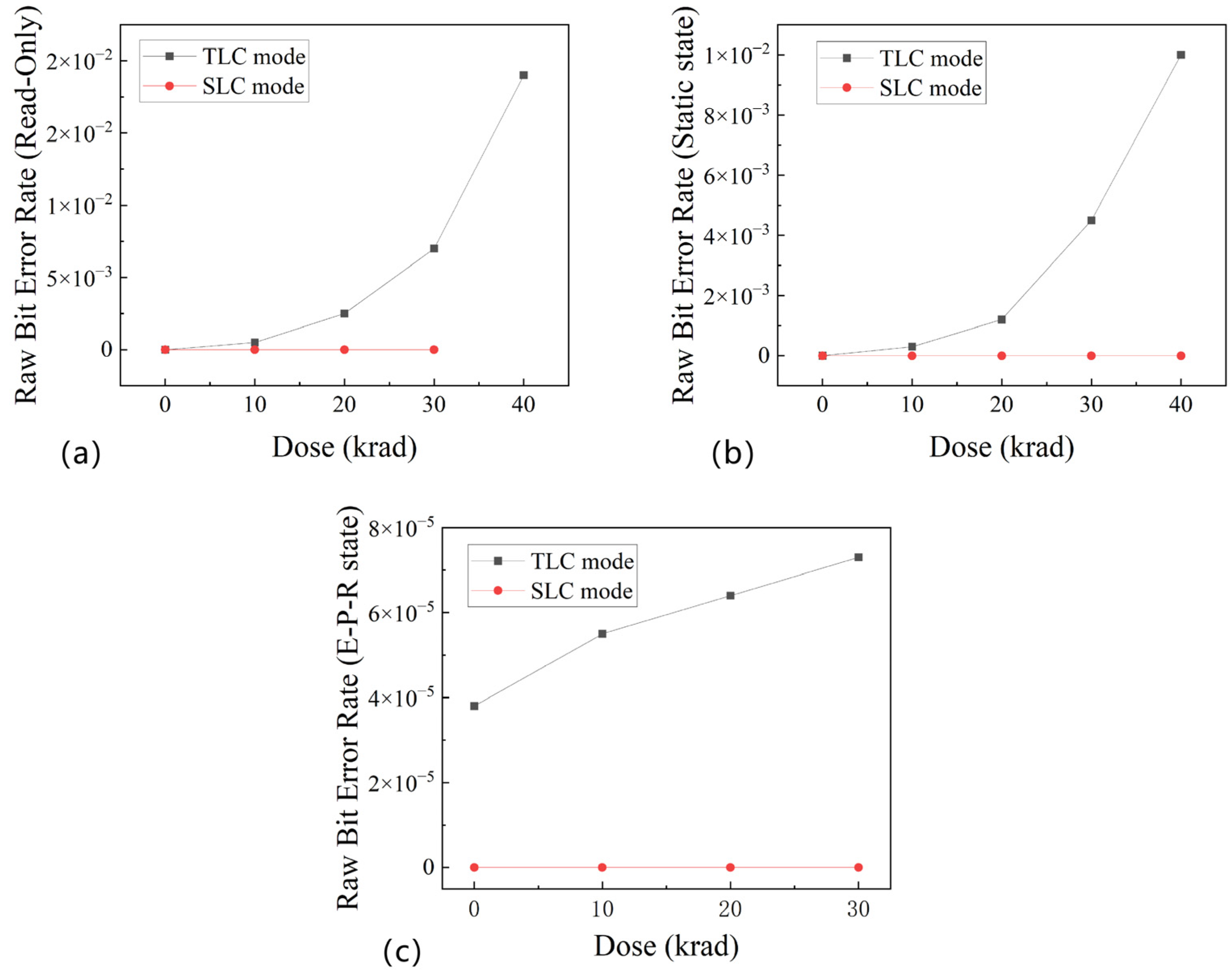
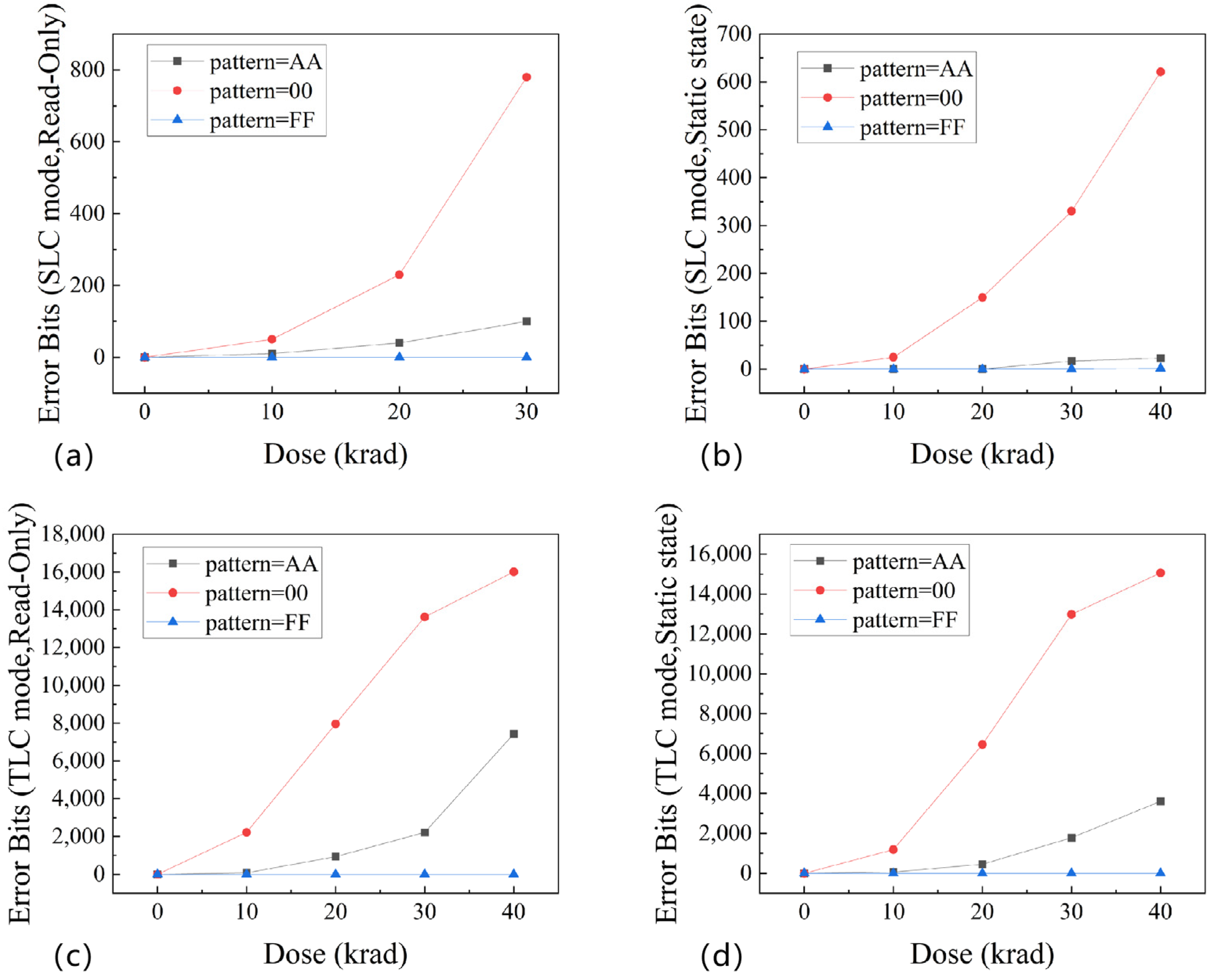
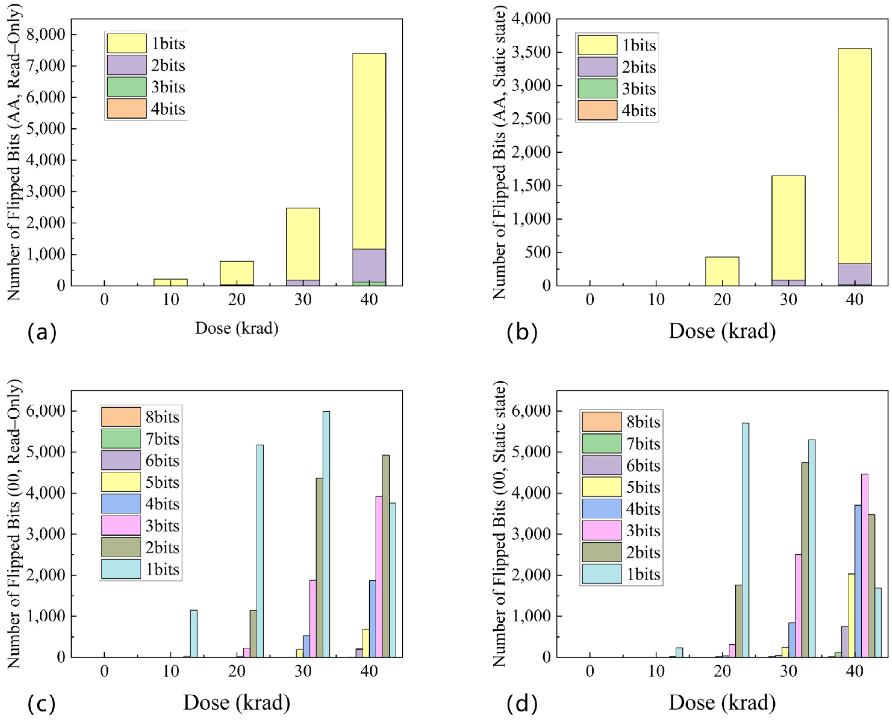
3. Results and Discussions

This section delineates the impact of radiation on NAND Flash memory performance, focusing on the raw bit error rate (RBER). The raw bit error rate refers to the bit error rate of flash memory without error correction code. In this work, we read data from the irradiated chip byte by btye and compared the collected data with the original data pattern to calculate the raw bit error rate. The following formula is used to compute the RBER:
RBER = Total   bit   error   counts   in   a   page Total   number   of   bits   in   the   page × 100 %
A. Raw Bit Error Rate
The RBER was assessed following TID irradiation, examining memory function under various operating modes, bias states, and data patterns.
Figure 2 illustrates the correlation between the RBER and dose under different operating modes and bias states. The analysis reveals that TLC mode exhibits a higher sensitivity to total dose effects. Initially, no bit errors were detected in TLC mode at a dose of 0 krad (Si). However, at a total dose of 10 krad (Si), bit errors began to manifest, with the rate of errors accelerating as the dose increased. In contrast, SLC mode demonstrated minimal bit errors, which remained significantly lower than those in TLC mode, even as the dose escalated. Compared with SLC mode, TLC mode has a greater threshold voltage distribution due to the extra programming state, which lead to the noise margin correctly identifying the cell states being smaller than in SLC mode. When the TID effect causes the programming state’s threshold voltage to shift, the flash operating in TLC mode will have more errors, resulting in an increase in the RBER.
The effect of radiation on memory also varies with bias states. Figure 3 displays the RBER–dose relationship under different bias states in both TLC and SLC modes. A comparison of the magnitudes in Figure 3a,b underscores the greater susceptibility of TLC mode to TID, aligning with the observations in Figure 2. Figure 3 illustrates that, irrespective of the operating mode, memory under the read-only state is most vulnerable to TID effects. Conversely, the erase–program–read cycle state exhibits the strongest resistance to TID effects. Compared with the static state, since the data of memory in the dynamic erase–program–read state are constantly updated, the corresponding RBER always displays initial error counts and has the lowest number of errors. However, the dynamic erase–program–read state will apply the maximum voltage in all of three bias states to the high voltage charge pump, and the combined action of repeated program/erase cycles and TID effect will lead to a lot of defects in the oxide layer. This means that the dynamic erase–program–read state has the lowest TID tolerance and fails when the radiation dose exceeds 30krad. The read-only bias state also repeatedly applies a voltage to the gate, and the charge is more likely to leak out of the charge trap layer compared to the static state. So, the memory in the read-only bias state has the highest RBER.
Further examination was conducted on the TID effects across three different data patterns (patterns = 00, AA, and FF). Figure 4 illustrates the bit error count for four scenarios. The radiation tolerance of Flash memory is influenced by the stored data pattern, with the 00 pattern being the most vulnerable to radiation and the FF pattern exhibiting almost no susceptibility to TID.
Comparative analysis with similar memory technologies revealed that 3D NAND’s performance, as reported in [20], indicates an RBER of approximately 0.1 in Multi-Level Cell (MLC) mode under read-only operation at a radiation dose of 40 krad (Si). In contrast, the RBER in SLC mode at the same radiation dose is 1e-5. Our findings demonstrate that at a radiation dose of 40 krad (Si), the RBER in TLC mode is 1 × 10⁻², and in SLC mode, it is 2 × 10⁻⁶, with both figures presenting an improvement over the results in [20]. Moreover, compared to the findings in [12,21], this memory exhibits superior bit error rate performance.
B. Standby current and read current
Figure 5a reveals an increase in the standby current of 3D NAND Flash memory post-irradiation across different operating modes. The TLC mode, particularly in read-only mode, displays the most pronounced increase in standby current, especially when the radiation dose exceeds 20 krad (Si).
Due to the out-of-tolerance standby current of flash memory after irradiation, we carried out an annealing test to study the effect of annealing time on the standby current of flash memory. In our work, the irradiated chips were placed at room temperature for two weeks and the standby current was measured every two days. The relationship between standby current and annealing time post-40 krad (Si) radiation is depicted in Figure 5b for the memory under TLC mode and read-only state. The figure demonstrates that as the annealing time extends, the standby current gradually diminishes and then stabilizes. When the annealing time exceeds 10 days, the standby current of the flash memory returns to the initial level. The TID effect introduces a large number of traps in the tunneling oxide layer of the memory, which strengthens the trap-assisted tunneling (TAT) mechanism. When the TID-induced trap state in the oxide was removed by the annealing test, the standby current of the memory decreased. Our findings can provide guidance for the optimal annealing time of CT 3D NAND Flash operating in radiation environments. Considering the time, cost, and memory annealing characteristics, we suggest that the optimal annealing time of the device is 7 days.
The cyclic read operation generates a consistent read current, the magnitude of which is recorded. Figure 6 presents the read current in relation to the dose, highlighting an increase in read current proportional to the dose. At a total dose of 40 krad (Si), the read current surges by approximately 1 mA, which means that this memory remains stable and reliable during the TID effect.
This memory exhibits robust TID resistance, especially in terms of standby current. When the chip is exposed to a radiation dose of less than 40 krad (Si), the change in standby current across all operational modes is below 15 uA, with an amplitude change under 25%, significantly lower than the figures reported in [12,17,18] under comparable conditions. At a dose of 40 krad (Si), the read current escalates from 6 mA to 7 mA, a variation that is less pronounced than that documented in [18]. Alterations in standby current are attributed to the formation of parasitic transistors and the shift in threshold voltage triggered by radiation [22].
C. Threshold voltage
We obtained the threshold voltage of memory by moving the reference voltage. In this work, Gamma irradiation was performed on the device with all pins grounded, and under SLC mode, the chips were irradiated up to 100 krad (Si). The relationship between the number of bit errors and the increment in bit errors of the memory and the reference voltage are shown in Figure 7; the latter can reflect the threshold voltage distribution of the memory cell. Figure 7a,b demonstrate a decline in the positive threshold voltage for pattern = 00 as the dose escalates. The threshold voltage distribution of the memory cell is Gaussian and the peak value decreases compared to before irradiation. Conversely, Figure 7c,d reveal that the negative threshold voltage for pattern = FF remains largely unaffected by TID.
Figure 8 showcases the failure thresholds of Flash memory across various operating modes (TLC/SLC) and bias states under TID effects. The bias states include read-only, static state, and dynamic erase–program–read cycles. Functional failure is identified when multiple pages are operated upon, and at least one page’s read-back data are entirely incorrect, rendering the data irrecoverable. The dynamic erase–program–read state exhibits the lowest failure threshold, highlighting its vulnerability to TID effects.
The experimental results reveal that for pattern = 00, the corresponding positive threshold voltage diminishes with increasing TID, aligning with prior research [23,24]. However, for pattern = FF, the results diverge. This study observes minimal impact from radiation, contradicting the existing literature where pattern = FF is also susceptible to TID [22]. The variation in threshold voltage is attributable to the change in charge in the charge trapping layer of the memory cell, with TID leading to charge loss [22,24,25].
D. Type of Bit Flip
Figure 9 shows the number of bit flips of CT 3D NAND Flash operating in TLC mode at different doses. In the case of radiation resulting in the loss of the same amount of charge, SLC mode will only appear with 0 becomes 1 bit flip, while for TLC mode, due to the characteristics of its programming state, both 0 becomes 1 and 1 becomes 0 can occur, i.e., there will be one or more flips when reading. For pattern = AA, as the dose increases, the frequency of flips also rises, predominantly manifesting as 1-bit flips without exceeding a 5-bit threshold, attributed to the exclusive occurrence of 0 becomes 1 flips. Conversely, in the context of pattern = 00, 1-bit flips are more prevalent at doses below 30 krad (Si), but higher doses lead to a predominance of multi-bit flipping. When the number of multi-bit flip bits exceeds 4 bits, this means that two adjacent cells are faulty.
The exclusive observation of 0 becomes 1 flips in this study contrasts with the findings reported in [26]. The incidence of bit errors in TLC mode exceeded that in SLC mode, aligning with the conclusions of [25]. Bit flipping is primarily caused by the loss of electrons from the memory cell’s charge trapping layer, a process exacerbated by radiation. This radiation damage leads to electron depletion and the emergence of uncompensated positive charges in the oxide layer, which facilitate the flipping of bits together.
E. Erase Block and Program Page Timing
Figure 10a,b demonstrate that the time required to erase a block decreases with the increasing dose in both SLC and TLC modes. Figure 10c shows an increase in program page time in TLC mode for doses exceeding 20 krad (Si). Figure 10d indicates that Flash operation in SLC mode remains unaffected by total dose effects below 30 krad (Si). However, when this threshold is exceeded, the program time operating in a static state will be reduced. Figure 10a–c highlight that the memory operating in a cyclic read state is the most vulnerable to radiation exposure.
Previous research [19] examined the TID effect on erase time, finding a decrease in erase time with increasing dose, aligning with our observations. Ref. [27] reported an escalation in program times with dose increases, a result echoed in our experiments where the program times at a 40 krad dose nearly doubled, exceeding the findings of [27]. This discrepancy is attributed to ionizing radiation not only inducing charge loss but also generating defect states at the interface, thereby altering the physical properties of both functional and defective cells. This alteration leads to variations in both erase and program times. Additionally, ionizing radiation impacts the peripheral circuits of 3D NAND memory [19]. In conjunction with other experimental outcomes, the variation in erase and program times can be attributed to the influence of TID on the peripheral circuits.
Overall, when compared to prior studies, this chip exhibits superior performance in terms of the RBER, standby current, and read current, showing minimal impact from TID radiation and presenting clear advantages. However, it does not demonstrate a distinct advantage in terms of positive threshold voltage shifts, block erase times, and page program times. Additionally, the negative threshold voltage remains largely unaffected by TID. Thus, the experimental findings confirm the memory’s robust TID resistance.

4. Conclusions

In our work, the impact of TID effects caused by Gamma rays on the performance of a 28nm 3D CT NAND Flash memory, operating in both TLC and SLC modes, was meticulously analyzed. The experimental data reveal that the RBER, standby current, and read operation current escalate with increasing doses, paralleled by a rise in the number of bit flips. This indicates that the severity of the TID effect intensifies with higher doses, adversely affecting memory performance. The threshold voltage’s decline with dose escalation is a critical factor contributing to the increase in the RBER. Moreover, threshold voltage shifts influence both erase and program times. Additionally, annealing time impacts performance, with some functionalities not reverting to pre-irradiation levels after annealing. Our work identifies the worst operating modes and bias states of a 28 nm 3D CT NAND Flash memory, which can provide guidance for spatial applications of this product. In the absence of capacity requirements, the optimal operating mode of this flash memory is SLC mode.

Author Contributions

The work presented here was completed via collaboration between all authors. Conceptualization, X.Z.; measurements and validation, X.Z., Y.W. and R.M.; formal analysis, X.Z, C.L. and T.W.; investigation, X.Z.; writing—original draft preparation, X.Z.; writing—review and editing, X.Z.; supervision, M.H.; project administration, L.X.; funding acquisition, X.Z. All authors have read and agreed to the published version of the manuscript.

Funding

This research received no external funding.

Data Availability Statement

Data are contained within the article.

Conflicts of Interest

The authors declare no conflicts of interest.

References

  1. Jooq, M.K.; Moaiyeri, M.H.; Al-Shidaifat, A.; Song, H. Ultra-efficient and robust auto-nonvolatile schmitt trigger-based latch design using ferroelectric CNTFET technology. IEEE Trans. Ultrason. Ferroelectr. Freq. Control 2022, 69, 1829–1840. [Google Scholar] [CrossRef] [PubMed]
  2. Cappelletti, P. Non volatile memory evolution and revolution. In Proceedings of the 2015 IEEE International Electron Devices Meeting (IEDM), Washington, DC, USA, 7–9 December 2015; pp. 10.11.11–10.11.14. [Google Scholar]
  3. Monzio Compagnoni, C.; Goda, A.; Spinelli, A.S.; Feeley, P.; Lacaita, A.L.; Visconti, A. Reviewing the Evolution of the NAND Flash Technology. Proc. IEEE 2017, 105, 1609–1633. [Google Scholar] [CrossRef]
  4. Lee, S.; Kim, C.; Kim, M.; Joe, S.-m.; Jang, J.; Kim, S.; Lee, K.; Kim, J.; Park, J.; Lee, H.-J. A 1Tb 4b/cell 64-stacked-WL 3D NAND flash memory with 12MB/s program throughput. In Proceedings of the 2018 IEEE International Solid-State Circuits Conference-(ISSCC), San Francisco, CA, USA, 11–15 February 2018; pp. 340–342. [Google Scholar]
  5. Tanaka, H.; Kido, M.; Yahashi, K.; Oomura, M.; Katsumata, R.; Kito, M.; Fukuzumi, Y.; Sato, M.; Nagata, Y.; Matsuoka, Y. Bit cost scalable technology with punch and plug process for ultra high density flash memory. In Proceedings of the 2007 IEEE Symposium on VLSI Technology, Kyoto, Japan, 12–14 June 2007; pp. 14–15. [Google Scholar]
  6. Jang, J.; Kim, H.-S.; Cho, W.; Cho, H.; Kim, J.; Shim, S.I.; Jeong, J.-H.; Son, B.-K.; Kim, D.W.; Shim, J.-J. Vertical cell array using TCAT (Terabit Cell Array Transistor) technology for ultra high density NAND flash memory. In Proceedings of the 2009 Symposium on VLSI Technology, Kyoto, Japan, 15–17 June 2009; pp. 192–193. [Google Scholar]
  7. Whang, S.; Lee, K.; Shin, D.; Kim, B.; Kim, M.; Bin, J.; Han, J.; Kim, S.; Lee, B.; Jung, Y. Novel 3-dimensional dual control-gate with surrounding floating-gate (DC-SF) NAND flash cell for 1Tb file storage application. In Proceedings of the 2010 International Electron Devices Meeting, San Francisco, CA, USA, 6–8 December 2010; pp. 29.27.21–29.27.24. [Google Scholar]
  8. Choi, E.-S.; Park, S.-K. Device considerations for high density and highly reliable 3D NAND flash cell in near future. In Proceedings of the 2012 International Electron Devices Meeting, San Francisco, CA, USA, 10–13 December 2012; pp. 9.4.1–9.4.4. [Google Scholar]
  9. Micheloni, R. 3D Flash Memories; Springer: Dordrecht, The Netherlands, 2016. [Google Scholar]
  10. Bagatin, M.; Gerardin, S.; Paccagnella, A.; Beltrami, S. Total Ionizing Dose Effects in 3D NAND Replacement Gate Flash Memory Cells. IEEE Trans. Nucl. Sci. 2023, 71, 412–417. [Google Scholar] [CrossRef]
  11. Kumari, P.; Huang, S.; Wasiolek, M.; Hattar, K.; Ray, B. Layer-Dependent Bit Error Variation in 3-D NAND Flash Under Ionizing Radiation. IEEE Trans. Nucl. Sci. 2020, 67, 2021–2027. [Google Scholar] [CrossRef]
  12. Bagatin, M.; Gerardin, S.; Paccagnella, A.; Beltrami, S.; Costantino, A.; Muschitiello, M.; Zadeh, A.; Ferlet-Cavrois, V. Total Ionizing Dose Effects in 3-D NAND Flash Memories. IEEE Trans. Nucl. Sci. 2019, 66, 48–53. [Google Scholar] [CrossRef]
  13. Kumar, M.A.; Raquibuzzaman, M.; Buddhanoy, M.; Wasiolek, M.; Hattar, K.; Boykin, T.; Ray, B. Total-Ionizing-Dose Effects on Threshold Voltage Distribution of 64-Layer 3D NAND Memories. In Proceedings of the 2022 IEEE Radiation Effects Data Workshop (REDW) (in Conjunction with 2022 NSREC), Provo, UT, USA, 18–22 July 2022; pp. 1–5. [Google Scholar]
  14. Schwank, J.R.; Shaneyfelt, M.R.; Fleetwood, D.M.; Felix, J.A.; Dodd, P.E.; Paillet, P.; Ferlet-Cavrois, V. Radiation Effects in MOS Oxides. IEEE Trans. Nucl. Sci. 2008, 55, 1833–1853. [Google Scholar] [CrossRef]
  15. Buddhanoy, M.; Kumari, P.; Surendranathan, U.; Wasiolek, M.; Hattar, K.; Ray, B. Total Ionizing Dose Effects on Long-Term Data Retention Characteristics of Commercial 3-D NAND Memories. IEEE Trans. Nucl. Sci. 2022, 69, 390–396. [Google Scholar] [CrossRef]
  16. Surendranathan, U.; Wasiolek, M.; Hattar, K.; Fleetwood, D.M.; Ray, B. Total Ionizing Dose Effects on Read Noise of MLC 3-D NAND Memories. IEEE Trans. Nucl. Sci. 2022, 69, 321–326. [Google Scholar] [CrossRef]
  17. Hu, H.; Feng, Y.; Zhan, X.; Xi, K.; Ji, L.; Chen, J.; Liu, J. Experimental characterizations on TID Radiation Impacts in Charge-trap 3D NAND Flash Memory. In Proceedings of the 2021 Silicon Nanoelectronics Workshop (SNW), Kyoto, Japan, 13 June 2021; pp. 1–2. [Google Scholar]
  18. Hansen, D.; Meraz, F.; Montoya, J.; Roberg, S.; Williamson, G. Radiation Testing of a Flash NAND Device. In Proceedings of the 2017 IEEE Radiation Effects Data Workshop (REDW), New Orleans, LA, USA, 17–21 July 2017; pp. 1–4. [Google Scholar]
  19. Buddhanoy, M.; Sakib, S.; Surendranathan, U.; Wasiolek, M.; Hattar, K.; Milenkovic, A.; Ray, B. New Total-Ionizing-Dose Resistant Data Storing Technique for NAND Flash Memory. IEEE Trans. Device Mater. Reliab. 2022, 22, 438–446. [Google Scholar] [CrossRef]
  20. Wilcox, E.P.; Campola, M.J. A TID and SEE characterization of multi-terabit COTS 3D NAND flash. In Proceedings of the 2019 IEEE Radiation Effects Data Workshop, San Antonio, TX, USA, 8–12 July 2019; pp. 1–7. [Google Scholar]
  21. Gadlage, M.J.; Bruce, D.I.; Ingalls, J.D.; Bossev, D.P.; McKinney, M.; Kay, M.J. Directional Dependence of Co-60 Irradiation on the Total Dose Response of Flash Memories. IEEE Trans. Nucl. Sci. 2019, 66, 148–154. [Google Scholar] [CrossRef]
  22. Bi, J. Radiation effects of floating-gate (FG) and charge-trapping (CT) Flash memory technologies. In Proceedings of the 2019 International Conference on IC Design and Technology (ICICDT), Suzhou, China, 17–19 June 2019; pp. 1–3. [Google Scholar]
  23. Bagatin, M.; Gerardin, S.; Paccagnella, A.; Beltrami, S. Depth Dependence of Threshold Voltage Shift in 3-D Flash Memories Exposed to X-Rays. IEEE Trans. Nucl. Sci. 2021, 68, 659–664. [Google Scholar] [CrossRef]
  24. Bagatin, M.; Gerardin, S.; Cellere, G.; Paccagnella, A.; Visconti, A.; Bonanomi, M.; Beltrami, S. Error Instability in Floating Gate Flash Memories Exposed to TID. IEEE Trans. Nucl. Sci. 2009, 56, 3267–3273. [Google Scholar] [CrossRef]
  25. Surendranathan, U.; Kumari, P.; Wasiolek, M.; Hattar, K.; Boykin, T.; Ray, B. Gamma-Ray-Induced Error Pattern Analysis for MLC 3-D NAND Flash Memories. IEEE Trans. Nucl. Sci. 2021, 68, 733–739. [Google Scholar] [CrossRef]
  26. Irom, F.; Nguyen, D.N.; Harboe-Sorensen, R.; Virtanen, A. Evaluation of Mechanisms in TID Degradation and SEE Susceptibility of Single- and Multi-Level High Density NAND Flash Memories. IEEE Trans. Nucl. Sci. 2011, 58, 2477–2482. [Google Scholar] [CrossRef]
  27. Allen, G.R.; Irom, F.; Edmonds, L.; Nguyen, D.; Scheick, L.Z.; Vartanian, S.; McClure, S.S.; Stanford, K. Total ionizing dose measurements of a commercial samsung NAND flash memory for a high dose mission. In Proceedings of the 2018 IEEE Radiation Effects Data Workshop (REDW), Waikoloa, HI, USA, 16–20 July 2018; pp. 1–9. [Google Scholar]
Figure 1. (a) A schematic of a 3D NAND Flash array. (b) A circuit diagram of a NAND Flash memory block.
Electronics 14 00473 g001
Figure 2. RBER under different operating modes in AA patterns. (a) RBER in read-only state. (b) RBER in static state. (c) RBER during dynamic erase–program–read state.
Electronics 14 00473 g002
Figure 3. RBER under different bias states in AA patterns. (a) RBER in SLC mode. (b) RBER in TLC mode.
Electronics 14 00473 g003
Figure 4. Bit errors for different data patterns. (a) SLC mode, read-only. (b) SLC mode, static state. (c) TLC mode, read-only. (d) TLC mode, static state.
Electronics 14 00473 g004
Figure 5. (a) Standby current across different operating modes and bias versus dose. (b) Standby current versus annealing time.
Electronics 14 00473 g005
Figure 6. Read current versus dose (SLC mode—read-only state).
Electronics 14 00473 g006
Figure 7. The relationship between the threshold voltage and radiation dose. (a) Pattern = 00, byte errors vs. reference voltage. (b) Pattern = 00, the increment in byte errors vs. reference voltage. (c) Pattern = FF, byte errors vs. reference voltage. (d) Pattern = FF, the increment in byte errors vs. reference voltage.
Electronics 14 00473 g007
Figure 8. The failure thresholds of Flash memory under varied operating conditions.
Electronics 14 00473 g008
Figure 9. The number of bit flips versus dose in TLC mode. (a) Pattern = AA, read-only. (b) Pattern = AA, static state. (c) Pattern = 00, read-only. (d) Pattern = 00, static state.
Electronics 14 00473 g009
Figure 10. Erase block and program page timing versus dose. (a) Erase block time in TLC mode. (b) Erase block time in SLC mode. (c) Program page time in TLC mode. (d) Program page time in SLC mode.
Electronics 14 00473 g010
Disclaimer/Publisher’s Note: The statements, opinions and data contained in all publications are solely those of the individual author(s) and contributor(s) and not of MDPI and/or the editor(s). MDPI and/or the editor(s) disclaim responsibility for any injury to people or property resulting from any ideas, methods, instructions or products referred to in the content.

