Abstract
Due to the restrictions of the operating environment and on-site space conditions, the energy routing devices used in Antarctic research stations must have a compact structure and require the internal power converter to have a high enough power density to reduce its size, so the internal DC/DC conversion link of the energy router adopts a two-stage voltage regulation scheme. In this paper, a Switched Tank Converter (STC) is used to realize the coarse voltage adjustment of the first stage. In order to further improve the power density of the STC, this paper integrates the half bridge with the same switching action in the STC, and several resonant slots share one inductor to obtain an H-bridge STC with reduced inductance. At the same time, an improved control method is proposed to solve the influence of passive device parameter error and the parasitic parameter on the resonant frequency by adjusting the on-time value of the switch on the rectifier side. This control method can effectively solve the influence of the passive device parameter difference on the converter without adding new devices, ensure the power density advantage of the converter, and improve efficiency. Finally, the validity and rationality of the circuit and the improved control method are verified by simulation and experiment. The experimental result shows that the H-bridge STC with reduced inductance has a power density of 1041 W/in3 at 600 W, which greatly improves the overall operating efficiency of the energy router.
1. Introduction
The energy router is the key equipment of the green and clean energy supply system of the Antarctic research station, and it is the hub that connects the source, storage, and load. The power electronic converter is the main power conversion device in the energy router, and it meets the requirements of high reliance and efficient operation, but it also requires a high power density, the size can be reduced, and it can be installed and operated in the tight-spaced polar energy router cabin.
DC/DC power conversion is the most widely used power conversion link in polar energy routers. Improving the power density is very important for the compact design and efficient operation of polar energy routers. For this reason, this paper draws on the 48 V bus bar power supply architecture proposed by Vicor (Andover, MA, USA) [1]. On this basis, the 48 V bus power supply architecture proposed in reference [2] significantly reduces the bus loss and weakens the influence of load mutation on the bus voltage and other loads. In this power supply architecture, 48 V voltage is supplied to the terminal load by the Voltage Regulator Module (VRM). We can design the VRM carefully to achieve high efficiency and high power density.
There are two existing VRM schemes: single-stage transformation and two-stage cascade transformation [3]. The single-stage scheme needs to realize high-proportion voltage conversion and precise control of the output voltage in the first-stage circuit, which is difficult to design. The two-stage scheme solves the design difficulty through the division of labor of cascade modules and has good scalability and transient performance. In a two-stage VRM, the Intermediate Bus Converter (IBC) is used to change the 48 V (40 V~60 V) DC bus voltage to the intermediate voltage (5 V~12 V), and then the second-stage adjustable load point converter accurately adjusts the output to 1 V~1.8 V according to the load demand. This two-stage structure is also known as the intermediate bus structure [4] because voltage regulation can be achieved through the second stage, and the first-stage IBC can use a fixed ratio buck converter, focusing on achieving high efficiency and high power density.
LLC Resonant Circuits [5], Phase-Shifted Full-Bridge Soft-Switching Circuits [6], and Non-Isolated Step-Down Circuits [7] can all be used as first-stage IBCs, but these circuits usually contain large magnetic components, resulting in large converter sizes and high power consumption. Using a switched capacitor converter (SCC) can eliminate magnetic components, thus improving power density, but it requires overcoming the constraints of charge redistribution loss [8]. In order to solve the problem of charge redistribution loss in SCC, references [9,10,11] added an inductor in an SCC to achieve resonance and soft charging operation, thus avoiding charge redistribution loss. In reference [12], a new topology of a switched capacitor converter was proposed, which reduces the power switch required and reduces the size of the converter to a certain extent while realizing Zero-Current Switching (ZCS). In reference [13], an inductor was introduced into a multi-level modular SCC to improve the controllability of resonance. On this basis, a simplified optimization was carried out in reference [14] to form a Switched Tank Converter (STC), which can be used as a first-level non-adjustable IBC in a two-level VRM structure.
In reference [2], an LLC resonant converter was adopted as the first-stage IBC, which integrates the transformer and inductor together, thereby improving the power density of the LLC and finally achieving a power density of 700 W/in3. Reference [14] proposed an SCC topology suitable for data centers as the first-stage IBC, which can achieve a step-down ratio of 6:1 and a power density of 750 W/in3. Based on the above topology, reference [15] optimized the switching devices, resonant inductors, and PCB layout to improve the power density and efficiency of the converter and finally realized the power density of 1000 W/in3.
In order to further improve the power density of the first-stage IBC in the two-stage VRM structure, this paper further improves the STC topology based on reference [14] and forms an H-bridge STC with reduced inductance, which greatly reduces the volume of the converter. In addition, the paper analyzes the influence of the passive device parameter difference on the STC’s efficiency in detail and proposes an improved control method based on it. This control method can effectively solve the influence of passive device parameter difference on the converter without adding new devices, ensure the power density advantage of the converter, and improve efficiency. Finally, the feasibility of an H-bridge STC with reduced inductance and the impact of the improved control method are confirmed by simulation and experiment.
2. Working Principle of Single-Inductance H-Bridge Switched Tank Converter (STC)
2.1. Derivation of Switched Tank Converte (STC) Topology of Single-Inductance H-Bridge
The STC circuit proposed in reference [16] is shown in Figure 1. The input/output ratio is 6:1; two complementary PWM signals, Φ1 and Φ2, with a 50% duty cycle, as shown in Figure 2, are used to control the on–off function of all switch tubes; and the switching frequency is equal to the resonant frequency.
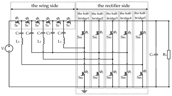
Figure 1.
Switched Tank Converter topology.
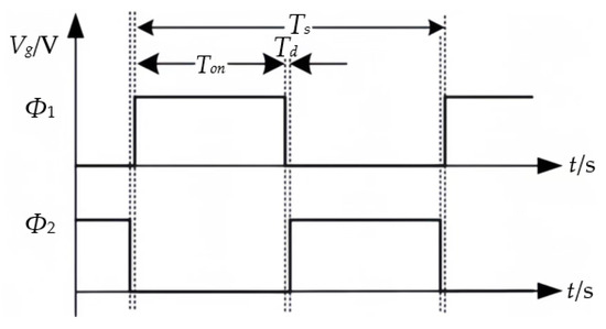
Figure 2.
Traditional PWM control signal.
Through the analysis of the working principle of the STC, it can be seen that the switch action of half bridges 1, 3, and 5 on the rectifier side is the same, and the switch action of half bridges 2 and 4 is the same; through separate integration, the H-bridge STC shown in Figure 3 can be obtained. After the above work, the number of switches in the circuit is greatly reduced, but the working principle and the voltage stress of the switch tube remain unchanged.
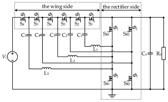
Figure 3.
H-bridge Switched Tank Converter (STC) topology.
Figure 4 shows the equivalent circuit of the H-bridge STC topology. There are three current loops in both states, and the arrows in the figure indicate the current flow direction. It can be seen that the three resonant branches work in the same way, and the resonant inductors L1, L3, and L5 have the same energy storage state, so the above inductors can be integrated into the common loop to share, and we can obtain the single-inductance H-bridge STC shown in Figure 5. When L = L1/3, the circuit before and after improvement can operate at the same switching frequency. The improved circuit not only avoids the influence of the difference in inductance parameters in the original circuit but also retains the advantage that all switch tubes can realize ZCS. And the reductions in the number of switches, the number of inductors, and the inductance value are conducive to improving the power density.
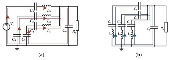
Figure 4.
Equivalent circuit of H-bridge STC: (a) signal Φ1 control; (b) signal Φ2 control.
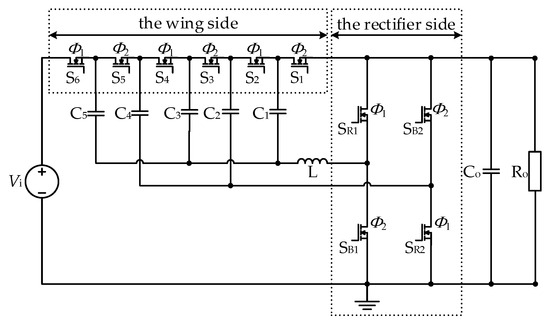
Figure 5.
Single-inductance H-bridge STC topology.
2.2. Working Principle of Single-Inductance H-Bridge STC Circuit
In the single-inductance H-bridge STC circuit which is shown in Figure 5, the resonant inductor L ensures the soft charging of the capacitor; considering its influence on the power density of the circuit, the inductance value of less than 100 nH is selected. C1, C3, and C5 are resonant with L, called resonant capacitors, and C1 = C3 = C5 = Cr; C2 and C4 do not participate in resonance and are called non-resonant capacitors, and C2 = C4 = Cnr. The circuit is still controlled by the PWM signals Φ1 and Φ2, as shown in Figure 2, and the switching frequency fs is equal to the resonant frequency fr calculated using Equation (1). At this time, Figure 6 shows the resonant inductor current waveform; the switching and resonant current commutation are carried out synchronously to ensure the ZCS in the switch tube and decrease the switching loss.
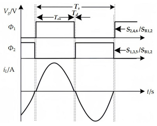
Figure 6.
Conventional PWM control and ideally inductor current waveform.
In the above equation, Cnreq stands for equivalent non-resonant capacitor and Creq stands for equivalent resonant capacitor. If we make the non-resonant capacitance value of the circuit much larger than the resonant capacitance value, that is, Cnr > 10 Cr, the impact of the non-resonant capacitance on the resonant frequency is negligible and can be ignored. At this time, Creq ≈ 3 Cr = C1 + C3 + C5, so the resonant frequency can be simplified as Equation (2).
According to the on–off time of the switch, the switches in Figure 5 are divided into two groups: A and B. Group A includes S6, S4, S2, SR1, and SR2, which are controlled by PWM signal Φ1; group B consists of S5, S3, S1, SB1, and SB2 and is controlled by the PWM signal Φ2. The working mode of ignoring dead time is analyzed as follows:
- Working mode 1: The group A switch is on, the group B switch is off, the input voltage source Vi charges the resonant capacitor C5 and output capacitor Co, and non-resonant capacitors C4 and C2 charge the resonant capacitors C3 and C1 and output capacitor Co, respectively. Figure 7a shows the equivalent circuit, the red lines in the figure are the circuit loops, and the arrows indicate the current flow direction.
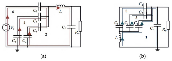 Figure 7. Equivalent circuit of single-inductance H-bridge STC: (a) working mode 1; (b) working mode 2.
 - Working mode 2: The group B switch is on, the group A switch is off, resonant capacitors C5 and C3 charge non-resonant capacitors C4 and C2 and output capacitor Co, respectively, and resonant capacitor C1 charges output capacitor Co. Figure 7b shows the equivalent circuit, the green lines in the figure are the circuit loops, and the arrows indicate the current flow direction.
Assuming the output voltage is Vo, because the inductance value is small, the average inductor voltage tends to be zero and can be ignored. In loop 1 of Figure 7, the average voltage of capacitor C1 is VC1 = VCo = Vo; similarly, in loop n (n = 2, 3, 4, 5) in Figure 7, VCn = VCn−1 +VCo = nVo, and the voltage present on capacitor Cn is the same as nVo. In loop 6, Vi = VC5 + VCo = 6Vo. So, the circuit can achieve a step-down ratio of 6:1.
2.3. Design of Resonant Element
In single-inductance H-bridge STC, resonant element design is closely related to the power density and efficiency of soft switches and circuits. For the design of resonant inductance, it is necessary to analyze the waveform of the inductor current and estimate the peak value of the inductor current to avoid core saturation. Assuming that the average output current of the STC is Io and its output part is directly connected to six switch tubes, the average current of each switch tube can be expressed by Equation (3). Because the current passing through the switch tube follows a half-period sine wave when the switch tube is on, the inductor current peak ILt-peak of the traditional STC can be expressed by Equation (4). The single-inductance H-bridge STC shares three inductors with the same operating state in the resonant circuit on the basis of the STC, so the inductor current in the single-inductance H-bridge STC is three times that of the conventional STC. Thus, the peak value ILH-peak of the inductor current in the single-inductance H-bridge STC can be derived from Equation (5), and then the inductor current iL(t) in the single-inductance H-bridge STC can be expressed by Equation (6).
For the design of a resonant capacitor, the main factors are voltage ripple and current capacity to ensure that the voltage and current of the resonant capacitor are within the safe range. According to the equivalent circuit in Figure 7a, the voltage vcn(t) (n = 1, 3, 5) and the peak-to-peak voltage Δvcn of the resonant capacitor can be calculated from the two differential equations of Equation (7), and the results are shown in Equation (8).
In the above equations, , and nVo represents the average voltage of the n (n = 1, 3, 5) resonant capacitor. It is clear from Equations (6) and (8) that the resonant inductor current and capacitor voltage ripple are related to the resonant inductance value, resonant frequency, and output power.
3. Influence of Parameter Error of Passive Device and Its Solution
3.1. Influence of Passive Device Parameter Error
In a single-inductance H-bridge STC, the switching frequency matches the resonant frequency ideally, in which case all switch tubes in the converter can achieve ZCS at the same switching frequency.
In the actual circuit, there are errors in the parameters of capacitance and inductance, so the switching frequency and the resonant frequency cannot be exactly equal, and the ZCS of the switch tube cannot be realized, and then the converter’s efficiency is influenced. Therefore, the problem of passive device parameter error needs to be solved urgently. When the resonant capacitance and inductance are less than the nominal value, the influence on the converter is greater [16]. Therefore, it is assumed that the resonant capacitance C3 and the inductance L are 10% less than the nominal value, respectively; at this time, the inductor current waveform under the traditional control method is shown in Figure 8. In the figure, states 1 and 4 are normal working states, and the resonant loop transmits power to the output end; since C3 and L are smaller than the nominal values, Equation (2) shows that the actual resonant frequency is bigger than the nominal resonant frequency, while the switching frequency equals the nominal resonant frequency, so the resonant current zero commutation is not synchronized with the switching state transition, as shown in states 2 and 5; states 3 and 6 indicate that when the dead zone time is too short, the inductor current cannot completely fall to zero before the next cycle is turned on, creating an energy cycle in the circuit that causes the converter’s conversion ratio to deviate from 6:1. Sufficient dead time can ensure that the current resets to zero. However, the energy cycle still results in higher losses in the converter and does not guarantee that the switch tube can achieve ZCS. Ref. [17] proposes using a zero-current detection sensor to evaluate the off state of the STC; this control method ensures that each resonant loop of the STC performs a separate ZCS operation but introduces additional devices that lead to a reduction in the converter power density.
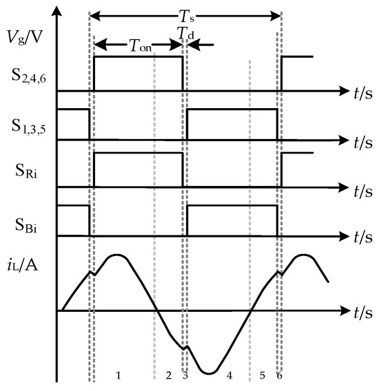
Figure 8.
Inductor current waveform under traditional control method.
3.2. Solution of Passive Device Parameter Error
Figure 9a shows the improved control sequence proposed in this paper. In this improved control sequence, switch tubes on the rectifier side of the single-inductance H-bridge STC is delayed at the on state for a period of time and turned off earlier than the wing side switch tubes.
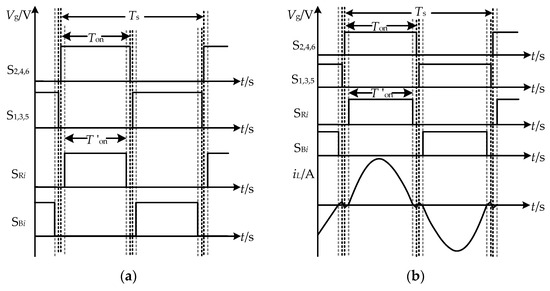
Figure 9.
The improved control method and inductor current waveforms: (a) the improved control sequence; (b) the inductor current waveform under the improved control method.
Figure 9b shows the inductor current waveform under the improved control method. When the forward inductor current reaches the zero point, the switch tubes SR1 and SR2 on the rectifier side are turned off; when the reverse inductor current reaches the zero point, the switch tubes SB1 and SB2 on the rectifier side are turned off to prevent the reverse flow of the inductor current, and thus, the energy cycle is suppressed and the efficiency of the converter is improved.
When the passive device parameter error is not considered, to prevent the inductor current from flowing backward, the on-time T′on value of the switch on the rectifier side can be calculated using Equation (10).
When the resonant capacitance C3 and the inductance L are 10% less than the nominal value, the discrepancy between the resonant frequency and the switching frequency is the most serious. So, in this situation, the on-time T′on value of the switch on the rectifier side can be calculated according to Equation (10).
In the above equation, Cr and L represent the rated resonant capacitance and resonant inductance values, respectively, and T represents the rated resonant period.
4. Device Selection
4.1. Switch Tube Power Loss Analysis and Selection
In a 48 V bus two-stage VRM, 54 V is usually used as the nominal input voltage, and the input voltage is limited to a maximum of 60 V. When the maximum input voltage of a single-inductance H-bridge STC is 60 V, the voltage stress applied to the switch tubes S2, S3, S4, and S5 is 20 V, and the voltage stress of other switch tubes is 10 V; the voltage stress applied to the switch tubes is the maximum, so the type of switch tube is considered in this situation.
The power loss of MOSFET includes gate drive loss, conduction loss, and switching loss. Gate drive loss is calculated using Equation (11) [14].
In the above equation, Vgs is the driving voltage of the MOSFET, Qg is the gate charge, and fs is the switching frequency. Conduction loss is calculated using Equation (12) [14].
In the equation, Rds(on) is the resistance of the MOSFET in the drain source conduction state, and irms is the effective value of the current passing through the drain source. Since the switch tube in the single-inductance H-bridge STC operates under ZCS, the switching loss is caused by the output capacitance Coss. When the MOSFET is off, the output capacitance is charged, and when the MOSFET is on, these charges are dissipated on the MOSFET. Therefore, the switching loss can be calculated using Equation (13) [14].
In the equation, Coss is the output capacitance of the MOSFET, and Vds is the drain-source voltage of the MOSFET. The total power loss of MOSFET is calculated using Equation (14).
Due to the large drain source on-resistance Rds(on) and output capacitance Coss of the high-rated voltage switch tube, which leads to large loss, we choose to use a 25 V or 30 V low-rated voltage MOSFET. In this paper, gallium nitride GaN FET EPC2023 with a rated voltage of 25 V from EPC (El Segundo, CA, USA) is selected for comparison with MOSFET BSZ013NE2LS5I with a rated voltage of 30 V from Infineon (Munich, Germany). The typical gate drive voltage of EPC2023 is 5 V, while the gate drive voltage range of Infineon Si MOSFET is wide, ranging from 0 V to 16 V [15]. Considering the two typical values of 5 V and 10 V, according to Equation (14), the power loss of EPC2023 and BSZ013NE2LS5I (using 5 V and 10 V gate drive voltages, respectively) is calculated, and the total power loss comparison diagram shown in Figure 10 is obtained. Table 1 shows the rated operating parameters of the two switch tubes.
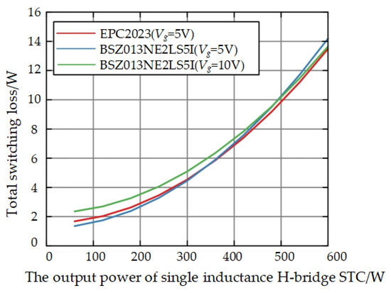
Figure 10.
Comparison of total power loss of MOSFET.

Table 1.
The rated operating parameters of the two MOSFETs.
By comparison, EPC2023 is selected as the wing switch tubes. Considering the higher current pass through the drain and source of the switch tubes on the rectifier side, BSZ013NE2LS5I with a 5 V gate drive voltage is selected as the switch tube on the rectifier side.
4.2. Capacitor and Inductor Selection
The type selection design of capacitors includes the design of resonant capacitors and non-resonant capacitors. In the design of resonant capacitors, the parameter error of the resonant capacitance causes a misalignment between the resonant frequency and the switching frequency, which affects the efficiency of the converter, so this paper selects a Class I ceramic capacitor with low dielectric loss and stable capacitance (dielectric material C0G). At the same time, considering the analysis of resonant capacitors’ voltage ripple in Section 2.3, the capacitor C2220C334J1GAC (Greenville, SC, USA) with a capacitance of 330 nF is selected as a Class I ceramic capacitor with a tolerance of only 5%. Considering that each capacitor can flow at a current of about 5 A, we choose to use six capacitors in parallel to form a resonant capacitor group.
The non-resonant capacitor is much larger than the resonant capacitor, which has little impact on the converter, so the Class II ceramic capacitor (dielectric material X7R) CGA6P1 × 7R1N106M250AC (Tokyo, Japan) with a capacitance of 10 μF is selected because its equivalent series resistance ESR is slightly larger than the others, so 12 capacitors are used in parallel to form a non-resonant capacitor group.
For the design of the inductor, in order to reduce the space ratio of the inductor as much as possible, the inductance value is less than 100 nH. According to the analysis of the inductor current in Section 2.3, the inductor model SLC7649S-360KLC (Mansfield, TX, USA) is selected by considering the inductance volume, rated current, and saturation current.
5. Simulation Analysis
Consider that in a 48 V bus bar two-stage VRM, 54 V is usually used as the nominal input voltage, and 60 V is the maximum input voltage. The rated power of the converter designed in this paper is 450 W, and the maximum power is 600 W, so in this section, we choose to conduct a simulation under the maximum power, and the simulated input voltage is 60 V.
In order to simulate the error of the capacitance and inductance values in the circuit under actual conditions, the inductance L and the capacitance C3 are decreased by 10% from their nominal values. Table 2 shows the simulation parameters of a single-inductance H-bridge STC.
Table 2.
H-bridge single-inductance simulation parameters.
When the input voltage is 60 V, the control sequence provided in Figure 6 is adopted, and the inductor current waveform in this case is shown in Figure 11. In the figure, the switch is switched after a period of time after inductor current zero commutation, and an energy cycle is generated in the circuit, resulting in the step-down ratio deviation of the converter.
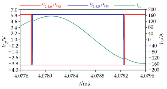
Figure 11.
Inductor current simulation waveforms under traditional control method.
Figure 12 displays the output voltage waveform in this situation; the output voltage is reduced to 8.5408 V, and the conversion ratio is 7:1.
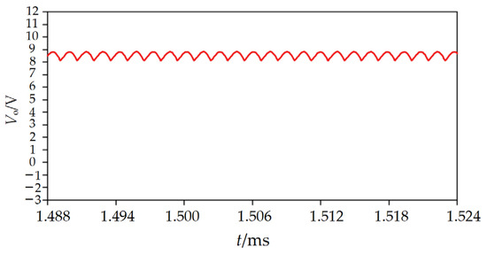
Figure 12.
Output voltage simulation waveform under traditional control method.
When we adopt the improved control method and the input voltage is 60 V, the inductor current waveform under the improved control method is provided in Figure 13, and switching is carried out synchronously with the inductor current commutation, avoiding the energy cycle. Figure 14 provides the output voltage simulation waveform. The output voltage is about 10 V, and the converter restores the conversion ratio of 6:1. The capacitor output voltage waveform under the improved control method is displayed in Figure 15. The average voltages of C5~C1 are 50 V, 40 V, 30 V, 20 V, and 10 V, equal to Vo, 2Vo, 3Vo, 4Vo, and 5Vo, respectively. It has been preliminarily verified that the improved control method can effectively solve the influence of passive device parameter error on the basic function of a single-inductance H-bridge STC.
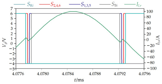
Figure 13.
Inductor current simulation waveform under improved control method.
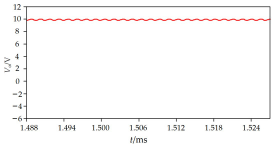
Figure 14.
Output voltage simulation waveform under improved control method.
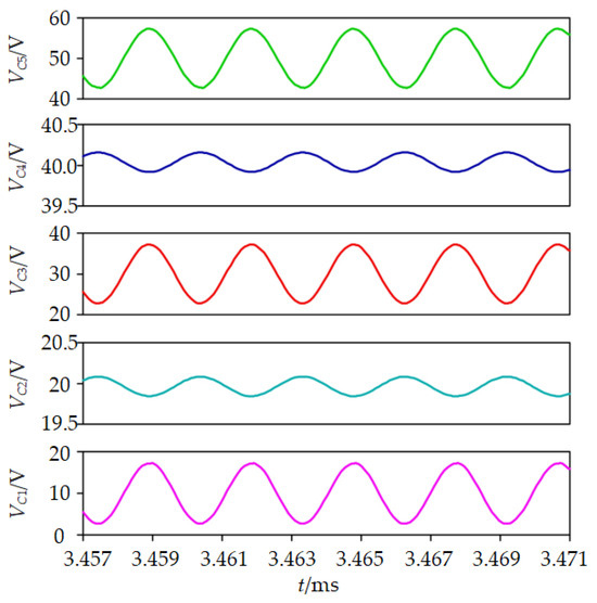
Figure 15.
Capacitor voltage simulation waveforms under improved control method.
6. Experimental Verification
6.1. Experimental Introduction
To further validate the effectiveness of the proposed circuit and the improved control method, a single-inductance H-bridge STC experimental platform is built in this section. The experimental platform is shown in Figure 16, and the experimental parameters are consistent with the simulation parameters in Table 3. When the input voltage is set to 60 V, the experimental waveforms under the traditional control method and the improved control method are observed. Through the analysis of the experimental waveforms, the effectiveness of the proposed converter and the improved control method is further verified.
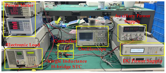
Figure 16.
The experimental platform.
Table 3.
Single-inductance H-bridge STC experimental parameters.
The single-inductance H-bridge STC hardware circuit board designed in this paper is shown in Figure 17a, with a size of 1.86 in × 1.24 in × 0.25 in. Figure 17b shows the 3D PCB comparison between a single-inductance H-bridge STC and STC.
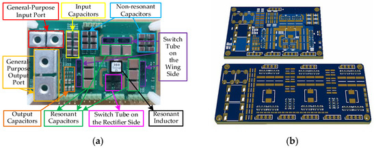
Figure 17.
Experimental circuit board: (a) single-inductance H-bridge STC hardware circuit board; (b) comparison of 3D PCB.
6.2. Experimental Verification Under Traditional Control Method
When the traditional control timing shown in Figure 6 is adopted, the grid drive voltage waveform of the switch tubes is the same or complementary symmetric with that of the switch tube S6, so only the grid drive voltage waveform of S6 is measured in this experiment. The experimental waveform is shown in Figure 18. Due to the error in the parameters of the passive device, the switching frequency does not match the resonant frequency. The switch tube is switched only after the inductor current has crossed zero and reversed for a period of time. At this time, the efficiency of the converter is only 84.1%. It is proven that the passive device parameter difference causes the circuit to produce an energy cycle and the switch tube cannot realize ZCS, which affects the efficiency of the converter.
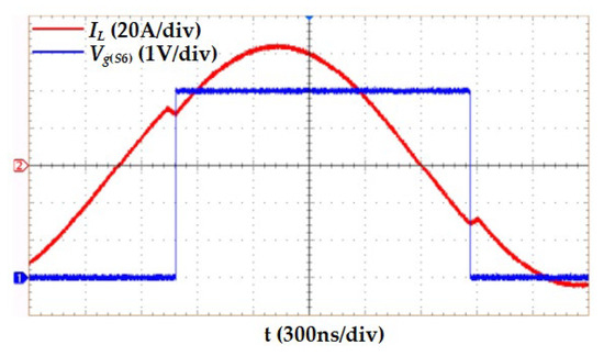
Figure 18.
Experimental waveform of inductor current under traditional control method.
The output voltage waveform under the traditional control method is shown in Figure 19. Due to the energy cycle in the circuit, great energy loss is caused, resulting in a serious deviation of the output voltage at about 8.4 V. The step-down ratio of the converter is 7.1:1. It can be seen that the difference in the parameters of passive devices under traditional control leads to the failure of the converter to achieve an accurate buck function.
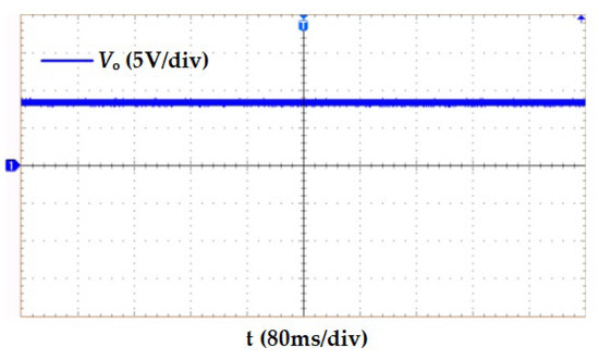
Figure 19.
Experimental waveform of output voltage under traditional control.
6.3. Experimental Verification Under Improved Control
According to the selection analysis in Section 4.2, the tolerance of the resonant inductance is ±10%, and the tolerance of the resonant capacitance is ±5%. When the resonant current crosses the zero reverse in advance, it will have a great impact on the converter.
According to Equation (15), the minimum on-time value of the rectifier side where the resonant current is not reversed can be calculated. Therefore, the on-time value of the switch tubes on the rectifier side is set as 1.36 µs in this paper.
Under the improved control timing sequence, the grid drive voltage waveform of the wing side switch tube is the same or complementary symmetrical with that of the switch tube S6, and the grid drive voltage waveform of the switch tube on the rectifier side is the same or complementary symmetrical with that of the switch tube SR1. Therefore, only the grid drive voltage waveform of S6 and SR1 is measured in the experiment. Figure 20 provides the experimental waveforms under the improved control method. At this time, the inductor current promptly returns to zero before opening in the next state, avoiding the energy cycle.
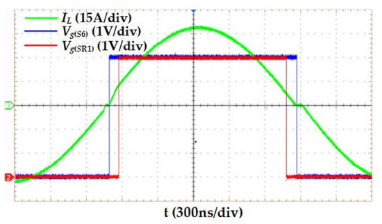
Figure 20.
Experimental waveform of output voltage under improved control method.
The voltage waveforms of the resonant capacitors are shown in Figure 21. The average voltages of the resonant capacitors C1, C3, and C5 are divided into 9.78 V, 29 V, and 49 V, which are equal to Vo, 3Vo, and 5Vo respectively. The voltage waveforms of the non-resonant capacitor are shown in Figure 22. The average voltages of the non-resonant capacitors C2 and C4 are 19.5 V and 39 V, respectively, which are equal to 2Vo and 4Vo, respectively. The experimental data confirm that the influence of the energy cycle on the circuit efficiency is avoided by using the improved control method, so the circuit can achieve a voltage reduction ratio of 6:1. At this time, the efficiency of the converter is 96.2%, and the power density of 1041 W/in3 at 600 W is increased by 41 W/in3 on the basis of reference [16].
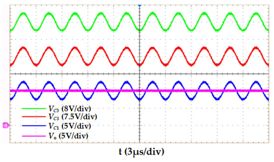
Figure 21.
Experimental waveforms of resonant capacitor voltage and output voltage under improved control.
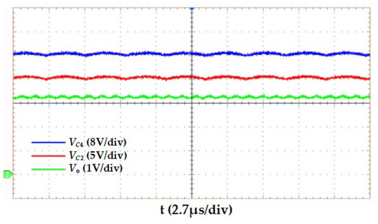
Figure 22.
Experimental waveforms of non-resonant capacitor voltage and output voltage under improved control.
The above experimental results show that the power density of the proposed single-inductance H-bridge STC is much higher than that of the STC. The improved control method can effectively reduce the energy cycle in the converter, reduce power loss, improve the efficiency of the converter, and guarantee the circuit realization of the 6:1 step-down ratio. At the same time, most of the converter switch tubes can realize ZCS.
7. Conclusions
In this paper, a new H-bridge switch slot converter with reduced inductance is proposed, which further improves the traditional STC circuit topology. At the same time, it integrates the half bridge with the same switching action and the inductors with the same operating state. In addition, in view of the effect of the passive device parameter error on circuit efficiency, an improved control method is proposed. The results show the following:
- The topology simplifies the number of switches and magnetic components and improves the power density, with a high power density of 1041 W/in3 at 600 W.
- The improved control method proposed in this paper can effectively solve the problem caused by the parameter error of passive devices and avoid the circulation in the circuit, thus reducing circuit loss and improving efficiency. The proposed single-inductance H-bridge STC circuit can achieve a step-down ratio of 6:1.
Author Contributions
Conceptualization, X.Y. and R.M.; Methodology, X.Y.; Software, X.Y.; Validation, X.Y. and R.L.; Formal Analysis, X.Y.; Investigation, X.Y., R.M., and R.L.; Resources, H.L., J.Z., and X.B.; Data Curation, X.Y.; Writing—Original Draft Preparation, X.Y.; Writing—Review and Editing, R.M.; Visualization, X.Y.; Supervision, H.L., J.Z., and X.B. All authors have read and agreed to the published version of the manuscript.
Funding
This research was funded by the Shanxi Energy Internet Research Institute, grant number SXEI2023A001; Shanxi Provincial Basic Research Program, grant number 20210302123170; and National Natural Science Foundation of China, grant number U23A20649.
Data Availability Statement
The data are contained within the article.
Acknowledgments
The authors thank the Major Research Support Project of Shanxi Energy Internet Research Institute (SXEI2023A001), the Basic Research Project of Shanxi Province (20210302123170); and the National Natural Science Foundation of China (U23A20649).
Conflicts of Interest
The authors declare no conflicts of interest.
References
- From 48 V Direct to Intel VR12.0: Saving ‘Big Data’ $500,000 per Data Center, per Year. Available online: https://www.mouser.com/pdfdocs/wp_VR12.pdf (accessed on 6 October 2024).
- Ahmed, M.H.; Fei, C.; Lee, F.C.; Li, Q. 48-V Voltage Regulator Module with PCB Winding Matrix Transformer for Future Data Centers. IEEE Trans. Ind. Electron. 2017, 64, 9302–9310. [Google Scholar] [CrossRef]
- Ren, X.Y.; Ruan, X.B. Two-stage Converter Applicable to High Voltage Input Low Voltage Output Case. Proc. CSEE 2005, 23, 153–157. [Google Scholar] [CrossRef]
- Ahmed, M.H.; Lee, F.C.; Li, Q. Two-stage 48-V VRM with Intermediate Bus Voltage Optimization for Data Centers. IEEE J. Emerg. Sel. Top. Power Electron. 2021, 9, 702–715. [Google Scholar] [CrossRef]
- Ahmed, M.H.; Lee, F.C.; Li, Q.; Rooij, M.d. Design Optimization of Unregulated LLC Converter with Integrated Magnetics for Two-stage 48V VRM. In Proceedings of the IEEE Energy Conversion Congress and Exposition (ECCE), Baltimore, MD, USA, 29 September–3 October 2019; pp. 521–528. [Google Scholar] [CrossRef]
- Zhou, S.L.; Tian, Y.T.; Bi, J.B.; Cheng, Y.H. Research on Phase-shifted Full-bridge DC/DC Converter Based on FB-ZVZCS. Power Electron. 2019, 53, 16–19. [Google Scholar]
- Zhang, Z.; Eberle, W.; Liu, Y.F.; Sen, P.C. A Novel Non-isolated ZVS Asymmetrical Buck Converter for 12 V Voltage Regulators. In Proceedings of the IEEE Power Electronics Specialists Conference, Rhodes, Greece, 15–19 June 2008; pp. 974–978. [Google Scholar] [CrossRef]
- Sano, K.; Fujita, H. Performance of a High-efficiency Switched-capacitor-based Resonant Converter with Phase-shift Control. IEEE Trans. Power Electron. 2010, 26, 344–354. [Google Scholar] [CrossRef]
- Yan, C.Z.; Yang, X.F.; Liu, Y.; Wen, P.; Zheng, T.; Chen, Q. Duty Cycle Optimization of Phase Shift Control Based on Resonant Switched Capacitor Converter. Trans. China Electrotech. Soc. 2021, 36, 676–687. [Google Scholar] [CrossRef]
- Li, Z.W.; Wu, X.Z.; Wang, J.; Qi, J.J.; Jing, L.; Xu, W.Z. Design of Magnetic Integrated Inductor for Resonant Switched Capacitor Converter. Trans. China Electrotech. Soc. 2022, 37, 6230–6238. [Google Scholar]
- Wen, P.; Yang, X.F.; Yan, C.L.; Zheng, T.; Igarashi, S.; Takaku, T. A SiC Modules Based Resonant Switched Capacitor Converter. Proc. CSEE 2020, 40, 8111–8122. [Google Scholar] [CrossRef]
- Abbasi, M.; Abbasi, E.; Tousi, B.; Gharehpetian, G.B. A Zero-current Switching Switched-capacitor DC-DC Converter with Reduction in Cost, Complexity and Size. Int. J. Circuit Theory Appl. 2019, 47, 1630–1644. [Google Scholar] [CrossRef]
- Li, Y.; Curuvija, B.; Lyu, X.; Cao, D. Multilevel Modular Switched-capacitor Resonant Converter with Voltage Regulation. In Proceedings of the IEEE Applied Power Electronics Conference and Exposition (APEC), Tampa, FL, USA, 26–30 March 2017; pp. 88–93. [Google Scholar] [CrossRef]
- Li, Y.; Lyu, X.; Cao, D.; Jiang, S.; Nan, C. A 98.55% Efficiency Switched-tank Converter for Data Center Application. IEEE Trans. Ind. Appl. 2018, 54, 6205–6222. [Google Scholar] [CrossRef]
- Lyu, X.; Li, Y.; Ren, N.; Nan, C.; Cao, D.; Jiang, S. Optimization of High-density and High-efficiency Switched-tank Converter for Data Center Applications. IEEE Trans. Ind. Electron. 2019, 67, 1626–1637. [Google Scholar] [CrossRef]
- Jong, O.; Li, Q.; Lee, F.C. Resonant Switched-capacitor Converter with Multi-resonant Frequencies. In Proceedings of the IEEE Applied Power Electronics Conference and Exposition (APEC), Anaheim, CA, USA, 17–21 March 2019; pp. 2177–2184. [Google Scholar] [CrossRef]
- Sovik, G.; Urkin, T.; Masandilov, E.E.; Peretz, M.M. Optimal Self-Tuning Control for Data-Centers 48V-12V ZCS-STC. In Proceedings of the IEEE Applied Power Electronics Conference and Exposition (APEC), New Orleans, LA, USA, 15–19 March 2020; pp. 455–462. [Google Scholar] [CrossRef]
Disclaimer/Publisher’s Note: The statements, opinions and data contained in all publications are solely those of the individual author(s) and contributor(s) and not of MDPI and/or the editor(s). MDPI and/or the editor(s) disclaim responsibility for any injury to people or property resulting from any ideas, methods, instructions or products referred to in the content. |
© 2025 by the authors. Licensee MDPI, Basel, Switzerland. This article is an open access article distributed under the terms and conditions of the Creative Commons Attribution (CC BY) license (https://creativecommons.org/licenses/by/4.0/).