You are currently viewing a new version of our website. To view the old version click .
Electronics
  • Article
  • Open Access

17 December 2025

A Design of 1.2–3.6 GHz Power Amplifier Based on Filters of Negative Feedback Network

,
,
,
,
,
and
1
Wuhan Qianyi Electronic Technology Co., Ltd., Wuhan 430205, China
2
Wuhan Bochang Communication Equipment Co., Ltd., Wuhan 430200, China
3
School of Electronic and Information Engineering, Nanjing University of Information Science & Technology, Nanjing 210044, China
4
School of Information Engineering, Xinjiang Institute of Technology, Aksu 843100, China
This article belongs to the Section Microwave and Wireless Communications

Abstract

This work proposes a broadband, high-efficiency extended continuous class-F (ECCF) power amplifier (PA) with a negative-feedback network structure. Compared with the traditional direct cascade connection of a PA and a filter, the design introduces a novel negative feedback filter structure. The transistor and filter synthesis network co-design method aims to compensate for the gain and efficiency drop of this PA in both high and low frequency bands, resulting in relatively flat gain and efficiency performance over a wide band. Consequently, there is a need to enhance the security and efficiency of wireless communication systems. This work verifies the proposed method using a designed and fabricated 10 W GaN HEMT device. The measured data reveal that the designed PA achieves 100% relative bandwidth from 1.2 GHz to 3.6 GHz, with a drain efficiency (DE) of 59.5~67.4%, an output power of 38.8~41.8 dBm, and a large signal gain of 8.8~11.8 dB.

1. Introduction

Driven by rapid progress in wireless communications [1,2,3,4], demand for high-performance RF PAs is escalating, and their relevance now extends to areas such as 100 MHz-level ultrasound imaging [5,6]. To meet the standards of next-generation wireless communication systems, including 5G, 6G, and beyond, RF amplifiers are required to have high efficiency, broadband, flat gain, and high linearity. Still, these amplifiers are prone to nonlinear distortion when working. The generation of these distorted signals needs to be filtered out by cascading high out-of-band suppression filters [7,8]. Compared with predistortion, the co-designed filtering structure reduces distortion without hardware and calibration complexity, maintaining broadband efficiency. However, designing the PA and filter separately will bring some problems. It will not only increase the area of the overall circuit but also cause partial energy loss, decrease the efficiency of the communication system, and increase the complexity of the design. In [9,10,11,12,13], a collaborative design method for PAs and filters, the so-called filtering PAs, is proposed.
Conventional PAs [14,15,16], including Class-B and Class-F designs, generally achieve high efficiency only over a narrow bandwidth because their performance depends on specific harmonic load impedance. To extend the high efficiency range of PAs, modes like Class-J, continuous Class-F, continuous Class-F−1, and a series of hybrid continuous modes have been developed to deliver high efficiency across a wide frequency range [17,18,19,20,21]. Recent CMOS PA advances, including Class-E architectures utilizing combined MOS devices to enhance efficiency, have shown promising results. However, their limited output power capability and relatively narrow bandwidth restrict their suitability for high-power wideband systems [22,23,24,25]. According to theory, the efficient bandwidth achievable by these continuous modes rarely exceeds one octave. The inability to attain multi-octave results from the high-order harmonic within the low-frequency band failing to overlap with the fundamental wave at higher frequencies. The ECCF mode PA can overcome the bandwidth limitation of one octave [26,27,28]. However, reported continuous Class-F PAs rarely address gain and efficiency flatness across the operating bandwidth. In the field of feedback amplifiers, refs. [29,30] propose a negative feedback network, respectively, aiming to balance the gain and efficiency differences between high and low frequencies. Figure 1a shows the conventional cascaded filtering PA. The proposed novel negative feedback filtering PA is shown in Figure 1b.
Figure 1. (a) Conventional cascaded filtering PA; (b) negative feedback filtering PA.
The 1.2–3.6 GHz band encompasses multiple sub-6 GHz wireless systems, but maintaining high efficiency and flat gain over such a broad range is limited by impedance variation and harmonic-tuning constraints. This paper proposes a novel negative feedback filtering PA, which is a co-design method of the filter network and PA transistor, which can not only suppress interference signals but also not affect the PA matching network’s impedance conversion to improve high-frequency gain and efficiency while reducing low-frequency gain and efficiency, thereby balancing the differences in gain and efficiency between high and low frequencies. Compared with classical DPD, the proposed co-designed negative feedback filtering technique eliminates the need for extra linearization hardware and complex calibration. By suppressing distortion directly inside the PA and compensating for gain and efficiency degradation across the band, it achieves flatter wideband performance with significantly reduced system complexity and power consumption. The fabricated 10 W GaN ECCF PA validates that high output power and efficiency are maintained over 1.2–3.6 GHz without using DPD, demonstrating strong advantages for compact and energy-efficient wideband transmitters. The approach proves both correctness and effectiveness, offering a new idea for designing broadband high-efficiency filtering PAs. The paper is structured as follows: Section 2 details the negative feedback network design, Section 3 covers ECCF theory, Section 4 presents the experimental setup and results, and Section 5 concludes.

2. Negative Feedback Filter Network

Although broadband impedance matching technology is diverse, it generally faces the dual constraints of limited impedance transformation amplitude and difficulty in bandwidth expansion. To overcome these limitations, designers often need to increase the network order to reduce the circuit quality factor Q value. However, this optimization path usually leads to the complexity of the circuit topology structure, and a trade-off between high-performance indicators and design feasibility is required. To solve the trade-off between bandwidth and high-order matching network, a filter network synthesis method [31,32] is proposed. This method is based on the filter matching network and uses the method outlined in [31,32] as its basis because it can achieve lower ripple and suppress harmonic distortion within the required bandwidth, thereby improving the overall circuit performance. In this design section, the matching network synthesis process can be divided into four main steps. Figure 2 illustrates the design flow in a stepwise graphical manner. The following content will introduce the specific implementation methods of each step in detail.
Figure 2. Filter structure design steps.
Step 1: According to the impedance transformation ratio, working bandwidth, center frequency, maximum available gain, and in-band ripple, the normalized original value is obtained, and the denormalization is performed according to the method given in [31] to obtain a real-to-real low-pass matching network. A high-order matching network is constructed by five pairs of LC resonant elements, and the initial network is shown in Figure 2.
Step 2: Reconstruct the parallel capacitor Cs1 by splitting the inductor L2 and the capacitor C4 into two miniature inductors and capacitors. Process the network elements L1, L21, and C1 obtained in step 1 to generate the parasitic output capacitance and parasitic inductance existing in the actual transistor. In addition, a T-Π circuit transformation [32] generates the parallel capacitor Cs1 and series inductor Lp. According to [33], the A parameter matrix of the framed T-type network is
A T = 1 ω 2 L 1 C 1 j ω ( L 1 + L 21 ) j ω 3 L 1 L 21 C 1 j ω C 1 1 ω 2 L 21 C 1
The A parameter matrix of the Π-type framed network is
A = 1 ω 2 L P C s 2 j ω L P j ω ( C s 1 + C S 2 ) j ω 3 C s 1 C s 2 L P 1 ω 2 L P C s 1
In order for the Π-type network to replace the T-type network, the A parameters of the two networks must be equal, that is
A T = A Π
In the equivalent circuit of T-Π, L1, L21, and C1 have obtained the initial values in step 1, so Lp is first calculated by Formula (3), and then Cs2 and Cs1 are calculated by Formula (3), respectively, so as to complete the T-Π equivalent transformation. However, it should be noted that when L2 is split into L21 and L22, L21 needs to be reasonably assigned to obtain the Cs1 required by the actual transistor.
For the framed Π-type network, the equivalent replacement of the Π-type concentrated parameters to the transmission line TL4 can be achieved by using the A parameter matrix equivalent method. The final replacement formula is
Z 4 = ω L 5 sin θ 4
θ 4 = arccos ( 1 L 5 C 5 ω 2 )
It should be noted that at this time, C4 = C41 + C42, and C42 = C5.
Step 3: Split LP into the parasitic package inductance Lp1 and the residual inductance LP2 in the actual transistor, and split Lt2 into LT and L6, and split L22 into Lt1 and Lt2 so that Lt1 = Lp2. Then C3 split into C31 and C32. The framed T-type structure on the left side is converted into a transmission line for welding of the actual transistor using the method of equivalent T-type network A parameters and transmission line A parameters, and the framed T-type network on the right side is converted into an equivalent Π-type network according to the method of step 2.
Step 4: In the package-level impedance matching design, it is necessary to comprehensively consider the influence of the optimal impedance and parasitic parameters, such as parasitic output capacitance and package inductance. For the package-level input and output impedance data obtained from the transistor, the parasitic parameter compensation can be achieved by adjusting Cs1 and Lp1 accordingly through the equivalent transformation method, thereby obtaining the actual usable matching network parameters.
R = R o p t 1 + ω 2 C s 1 2 R o p t 2
X = ω ( L P 1 C s 1 R o p t 2 )
After completing the above steps, parasitic output capacitance and package inductance of the transistor are incorporated to improve the high-order low-pass filter network. At higher frequencies, where lumped elements tend to exhibit transmission line behavior, this modification ensures accurate analysis and performance. Relative to standard high-order filters, the proposed network also achieves a more compact layout.
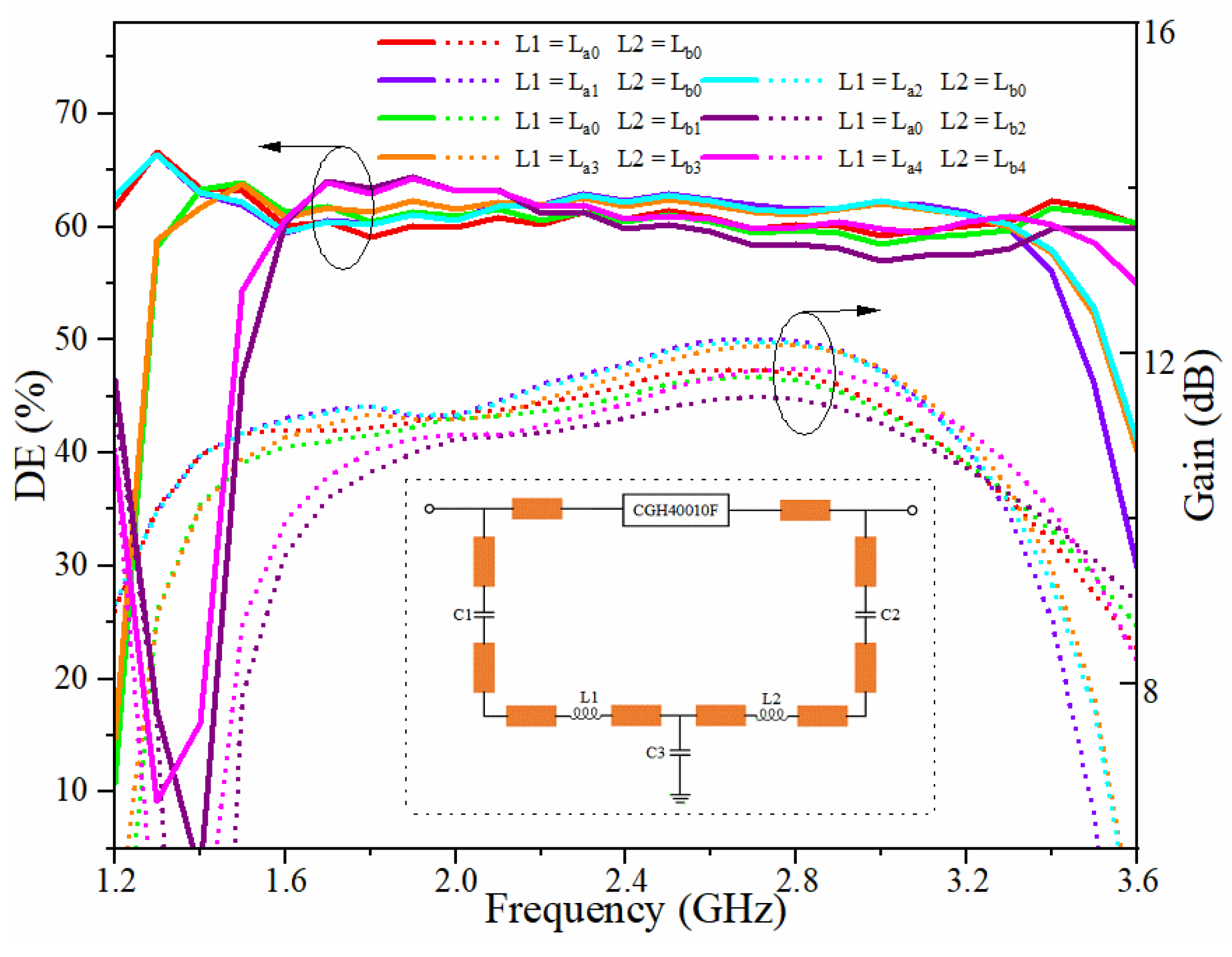
Negative feedback feeds a signal from a transistor’s output (drain) back to its input (gate). Negative feedback operates by subtracting the feedback signal with respect to the input. A resistance and a capacitance positioned between the gate and drain form the typical negative feedback structure. In Figure 3, a new type of negative feedback network is developed in this work. Capacitance C3 is introduced to the designed circuit, grounding a portion of the negative feedback path. In the proposed feedback network, C3 is grounded to partially divert the feedback signal, controlling its strength and balancing it across the bandwidth. This improves gain and efficiency flatness, enhances stability, and together with C1 and C2 maintains DC isolation while limiting excessive high-frequency feedback to the transistor gate. This facilitates the implementation of a broadband PA. Two capacitances form the feedback network connecting the drain and gate of the transistor are C1 and C2, and two inductances are L1 and L2. Capacitance C1 acts to isolate the DC voltage across the drain-to-gate path. It also tunes the coupled RF signal across the drain-to-gate path, while C2 blocks high-frequency components from reaching the gate, enhancing feedback stability. As shown in Figure 3, L1 and L2 can tune the efficiency and gain of the PA within the working bands at high- and low-frequency bands, respectively. At this time, the red solid/dashed line is the best feedback status.
Figure 3. Effects of different L1 and L2 on DE and gain in negative feedback network.

3. Theory of ECCF PA

The conventional Class-F PA is based on the Class-B PA model. Proper loading of the active device’s output controls the fundamental and harmonic components to form the desired waveform. With the ECCF PA [34], the bandwidth extends beyond one octave, and the impedance is given by
V ECCF = ( 1 2 3 cos θ ) 2 ( 1 + 1 3 cos θ ) ( 1 γ sin θ ) ( 1 + δ cos θ )
I ECCF = 1 π + 1 2 cos θ + 2 3 π cos 2 θ +
D E = π ( 2 3 δ ) 4 4 3 δ
Z f E C C F = ( 2 3 δ ) R o p t + j ( 1 7 12 3 ) R o p t γ
Z 2 f E C C F = 3 π 8 ( 5 3 3 R o p t δ j ( 7 3 3 δ ) R o p t γ )
Z 3 f E C C F =
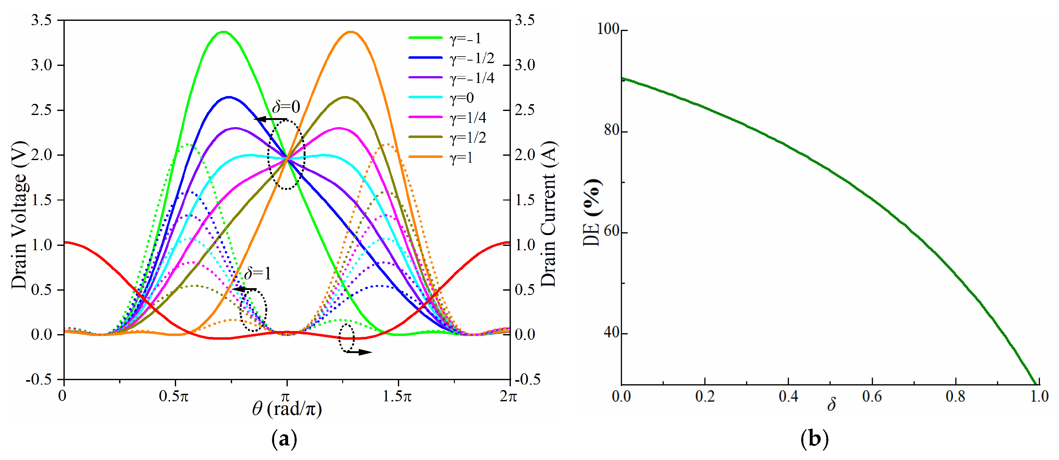
According to the above formulas for drain voltage and current (8), (9), the corresponding waveforms as the parameters δ and γ change can be plotted, illustrated in Figure 4a. Based on the normalized drain current and voltage expressions of the ECCF PA, we can deduce that when γ = 0 and δ = 0, the normalized voltage waveform corresponds to that of the Class-F PA. At this point, the overlap area between the voltage and current waveforms is minimal, thus resulting in the highest efficiency. When δ = 1, corresponding to the dashed line portion in Figure 4a, it can be seen that the voltage waveform decreases to some extent.
Figure 4. (a) ECCF drain current and voltage waveform; (b) DE as a function of δ.
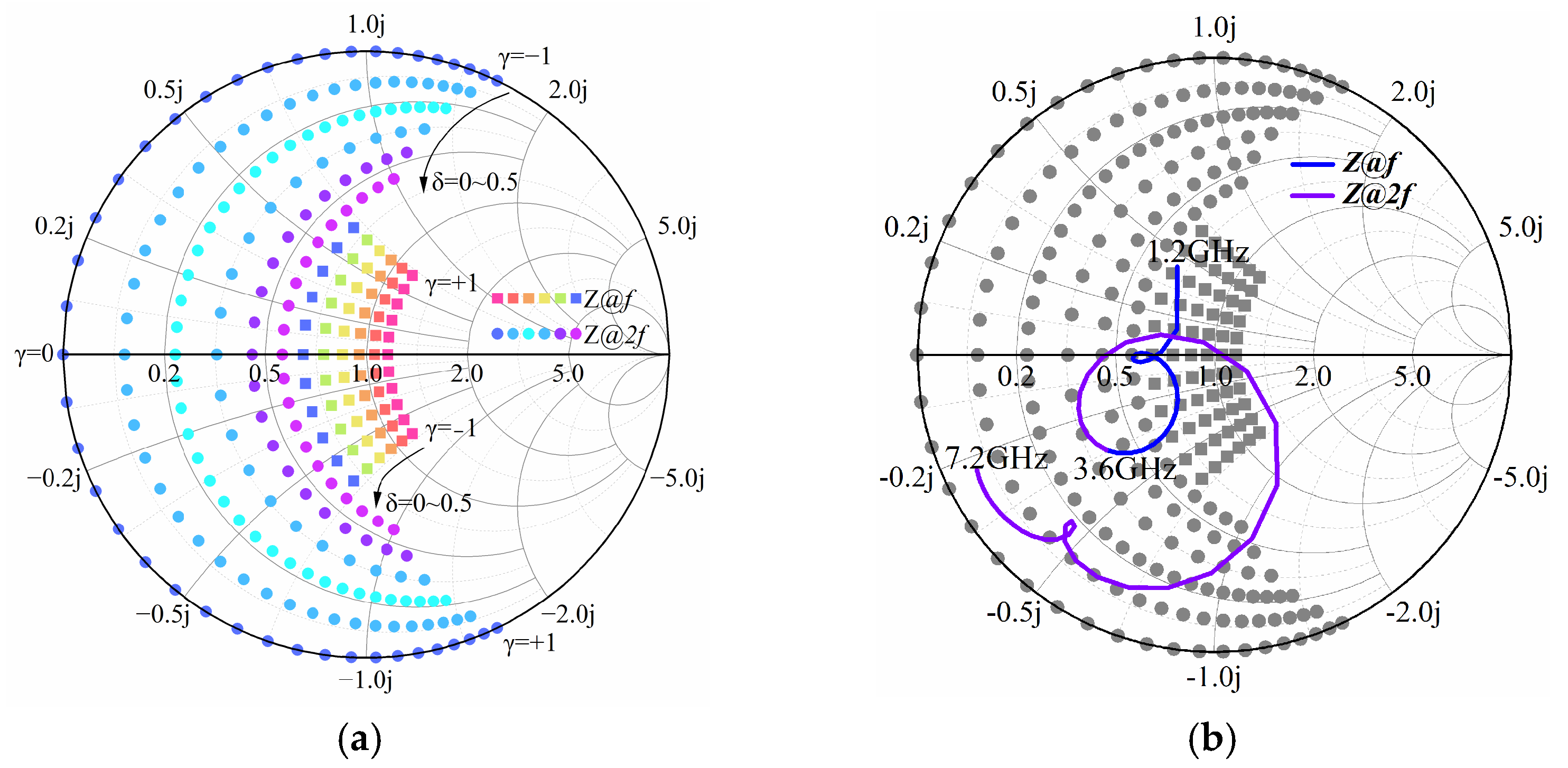
Using Formula (10) for DE, Figure 4b is obtained. As the value of δ changes, the voltage and current alternation area also changes, expanding the bandwidth at the expense of some efficiency. Figure 4b shows that when δ is less than 0.7, the DE ranges from 60% to 90.7%. Fundamental and harmonic impedances of the ECCF PA are derived by varying γ from −1 to 1 and δ from 0 to 1, as depicted in Figure 5a.
Figure 5. (a) Fundamental and second harmonic impedance mapping of ECCF modes; (b) simulated impedance trajectory of the output matching network on the I-gen plane.
Mapping the impedance expressions (11)–(13) onto the Smith chart allows the ECCF PA impedance design space to be plotted on the I-gen plane, as illustrated in Figure 5a. Observation shows that when δ is limited between 0.5~1, the fundamental frequency and second resistance begin to overlap, leading to a notable increase in the impedance region. Therefore, the design problem of multi-bandwidth PAs arising from the overlap of fundamental and harmonic frequencies can be solved. Figure 5b presents the fundamental and second-harmonic impedance distribution of the output matching network on the I-gen plane. The blue line shows the fundamental impedance trajectory, while the purple line indicates the second harmonic trajectory. Most of these traces fall within the optimal impedance region.

4. Implementation and Measurement

This section discusses the design of an ECCF PA using a 10 W GaN HEMT device CGH40010F from Wolfspeed. The gate and drain voltages are set to −3 V and 28 V, respectively. For demonstration, the proposed broadband ECCF PA is implemented using a Rogers 4350B substrate (ɛr = 3.66, H = 30 mil).
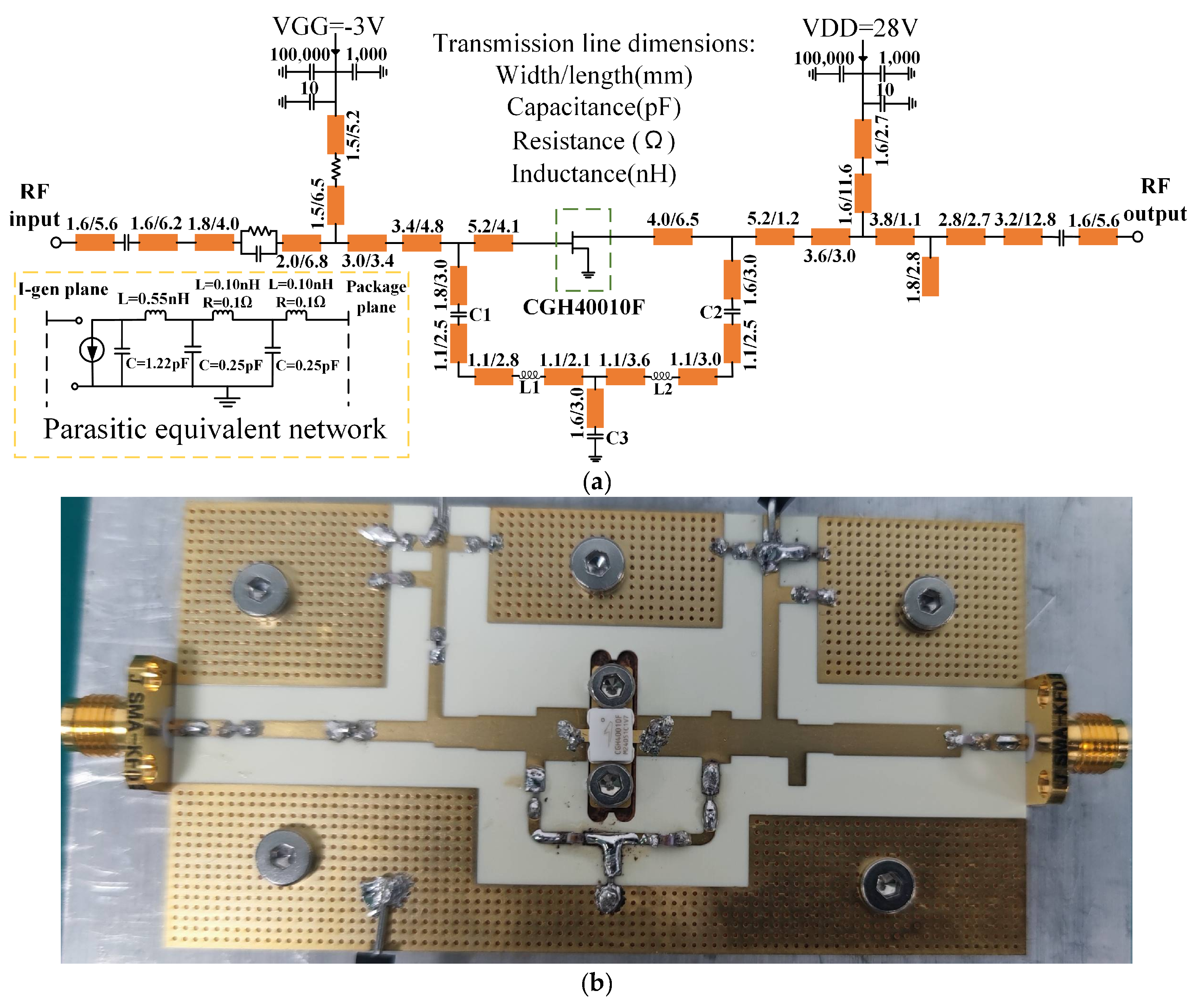
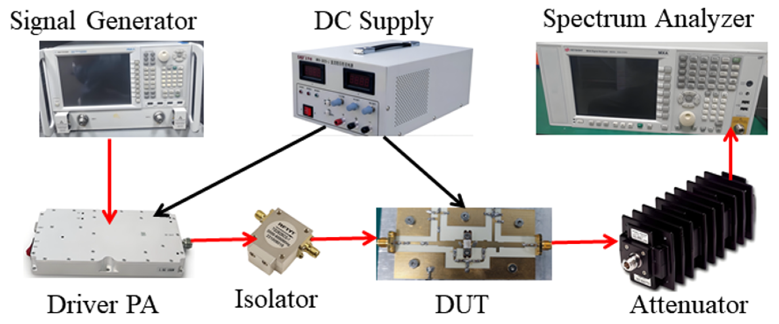
A comprehensive multiple-simulation flow was utilized to guarantee the broadband performance of the proposed PA. The frequency sweep was conducted from 0.5 to 4.0 GHz with a 0.1 GHz step and an input power level of 30 dBm. First, DC characterization and bias design were completed through DC sweep analysis. Source-pull and load-pull simulations were then employed to determine the optimal input and output impedance conditions. Large-signal S-parameter and harmonic balance simulations were performed to evaluate gain, efficiency, and harmonic tuning behavior. After obtaining a preliminary matching structure, the design was translated into a microstrip-based layout, where EM simulations using ADS Momentum were conducted to incorporate transmission-line dispersion, coupling, and parasitic effects. Finally, schematic-layout co-simulation validated that the integrated implementation meets the intended broadband high-efficiency design objectives. Figure 6a presents the ECCF PA schematic along with the equivalent circuit representing the transistor package’s output parasites, while Figure 6b shows the fabricated PA. As depicted in Figure 7, the DUT was characterized using an RF signal generator, isolator, DC power supply, attenuator, and spectrum analyzer. Input signals were amplified to the required level, and the measured output power was then used to calculate performance metrics.
Figure 6. (a) Designed PA circuit diagram; (b) visual of the assembled PA prototype.
Figure 7. Test setup for the proposed PA.
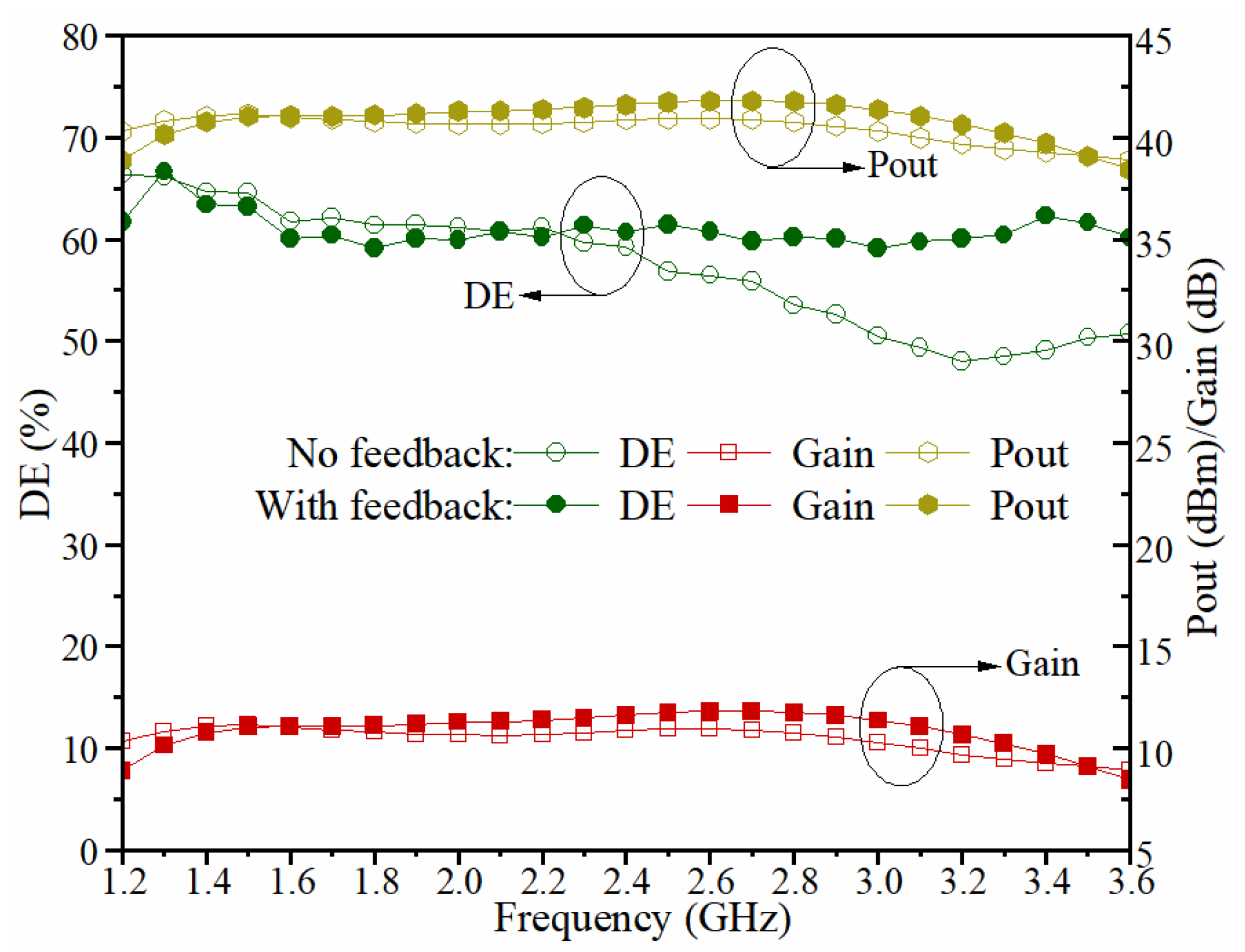
The effect of negative feedback on the ECCF PA is illustrated through simulation results in Figure 8, showing improved performance with the feedback structure. To examine the designed PA’s performance in more detail, Figure 9 shows the simulated and measured DE, Pout, and gain across the full operating bandwidth under continuous-wave excitation. Figure 9 demonstrates that in the 1.2~3.6 GHz frequency band with a relative bandwidth of 100%, the test results show that a saturated Pout of 38.4–41.8 dBm is provided, and its gain is 8.8–11.8 dB, and the DE is between 59.5% and 67.4%. At this time, the efficiency and gain remain relatively flat. This fully demonstrates that the performance of this power amplifier is fully utilized. In addition, as can be seen from Figure 9, regarding gain and output power, the measurement and simulation results are basically consistent.
Figure 8. Simulated DE, gain, and output power of the ECCF PA with versus without negative feedback.
Figure 9. Simulated and experimental DE, gain, and output power across frequency.
Figure 10 depicts the correlation between the DE and the gain measured at different frequency points and the resulting output power. In addition, as shown in Figure 10 that with respect to gain and Pout, the measured values are in good agreement with the simulated values. To evaluate the dynamic characteristics within the bandwidth range of 1.2 GHz to 3.6 GHz, we specifically selected six frequency points of 1.2, 1.6, 2.0, 2.4, 3.0, and 3.6 GHz for measurement. Figure 10 demonstrates that the six selected frequencies perform well across different input signal levels. This good performance is attributed to the use of a negative feedback structure, where the optimal performance occurs with a DE of 67.4% and a gain of 10.7 dB.
Figure 10. DE and gain measurements versus input power across different frequencies.
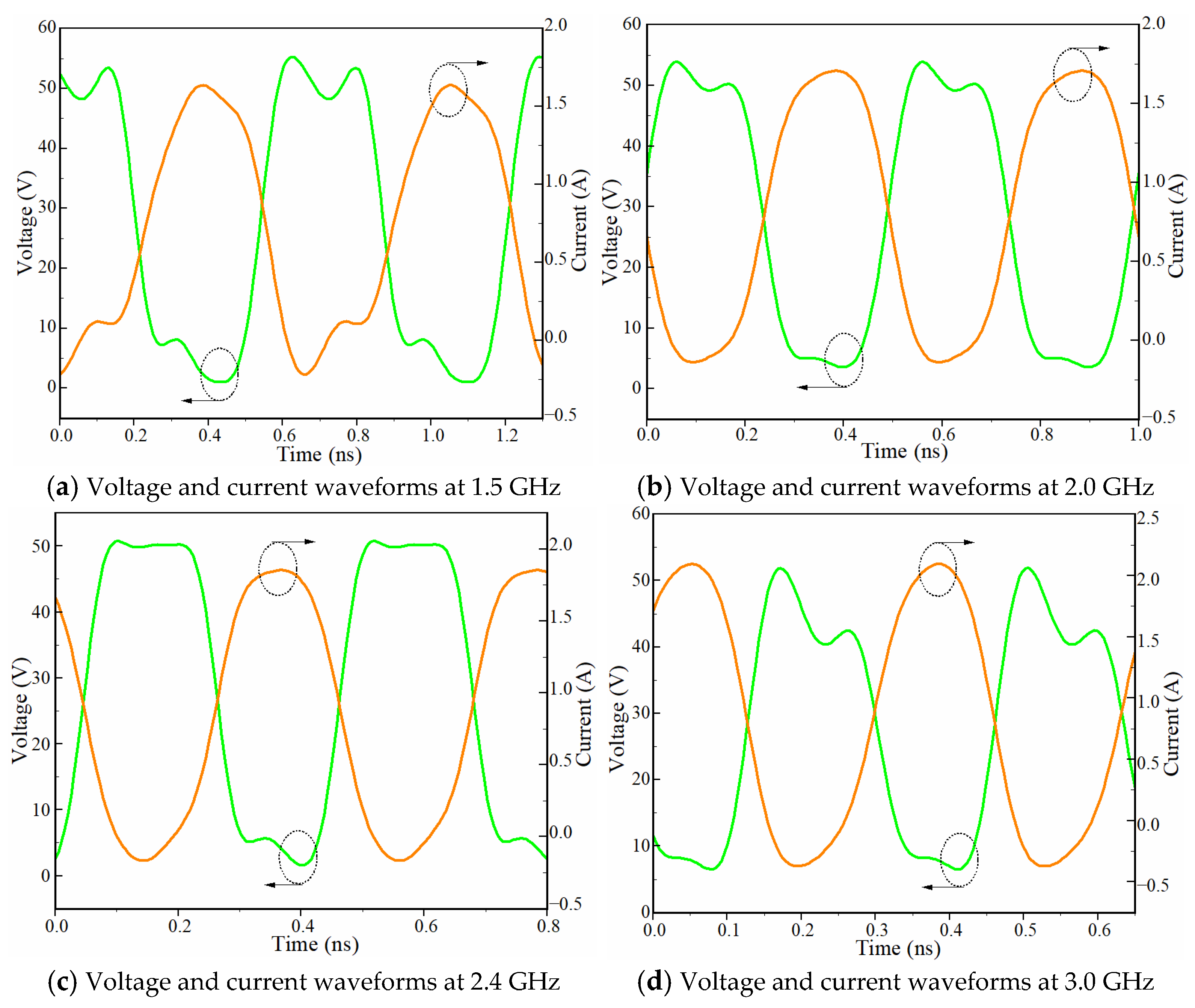
Figure 11 plots the drain voltage and current waveforms over four distinct frequencies. It can be concluded from the waveforms at specific frequencies that the voltage exhibits an almost square shape, whereas the current shows a near half-sine profile, indicating a Class F operating mode. In addition, the staggered voltage and current distribution lowers drain energy loss, facilitating high-efficiency operation of a wideband PA. In summary, this design verifies the rationality of the proposed method.
Figure 11. Intrinsic drain voltage plane and current waveforms obtained from simulation at (a) 1.5 GHz, (b) 2.0 GHz, (c) 2.4 GHz, (d) 3.0 GHz, respectively. The orange lines represent the current, and the green lines represent the voltage.
Compared with conventional PA filter cascades [7,10,11], the proposed co-designed negative feedback filter network eliminates additional parasitic output capacitance and package inductance, enabling improved high-frequency gain and efficiency and moderated low-frequency response for more balanced broadband performance. The proposed PA’s performance is benchmarked against the PAs presented in Table 1. Over a wider frequency range, flatter performance in both output power and efficiency is achieved by the proposed PA. Table 1 demonstrates that the proposed PA maintains output power and gain while achieving the widest frequency band.
Table 1. Comparison with the existing literature.

5. Conclusions

This study introduces a PA design method with a negative feedback filter network. The filter synthesis network is designed in coordination with the PA transistor, which can not only achieve impedance transformation without affecting the output matching network of the PA but also suppress the low-band gain and efficiency while enhancing the high-band gain and efficiency, thereby balancing the difference in gain and efficiency between high and low frequencies. An ECCF PA with broadband and high-efficiency functioning at 1.2–3.6 GHz was developed and prepared. The correctness and effectiveness of this method were verified based on the good performance of the test, providing a new idea for the engineering broadband PAs with high efficiency with negative feedback. Therefore, it is essential to improve the security and effectiveness of the wireless communication infrastructure.

Author Contributions

Methodology, Z.Y. and C.C.; software, Z.M. and Z.D.; formal analysis, Q.F. and X.W.; supervision, Z.C. All authors have read and agreed to the published version of the manuscript.

Funding

This paper was supported by the Project of Zhejiang Provincial Science and Technology plan (Grant 2024C01076), Project of Ministry of Science and Technology (Grant D20011) and Shanxi Provincial Science and Technology plan (Grant 2023-ZDLGY-49).

Data Availability Statement

The data presented in this study in available on request from the corresponding author.

Conflicts of Interest

Authors Zhenghao Yang, Quanbin Fu and Xiaogang Wang were employed by the company Wuhan Qianyi Electronic Technology Co., Ltd. Authors Chucai Cai, Zhengxian Meng and Zhiyong Ding were employed by the company Wuhan Bochang Communication Equipment Co., Ltd. The remaining author declares that the research was conducted in the absence of any commercial or financial relationships that could be construed as a potential conflict of interest.

References

  1. Liu, S.; Pang, J.; Gao, R.; Dai, Z.; Li, M.; Chen, S. Highly-Efficient Broadband GaAs HBT Doherty Power Amplifier with Harmonic Control Technique for 5G Application. IEEE Trans. Circuits Syst. II Express Briefs 2025, 72, 713–717. [Google Scholar] [CrossRef]
  2. Kostrzewska, K.; Kryszkiewicz, P. Power Amplifier Modeling Framework for Front-End-Aware Next-Generation Wireless Networks. Electronics 2024, 13, 1643. [Google Scholar] [CrossRef]
  3. Mehter, E.; Üçüncü, M. Radio Frequency (RF) Power Amplifier Design Providing High Power Efficiency in a Wide Dynamic Range. Electronics 2025, 14, 1435. [Google Scholar] [CrossRef]
  4. Li, C.; Zhang, Z.; Su, X.; Li, Y.; Liang, X.; Pei, Y.; Chen, C.; Xu, Y. Compact Internally Matched High-Power Power Amplifier with a Wide Frequency Band of 0.8–2 GHz. Electronics 2024, 13, 2687. [Google Scholar] [CrossRef]
  5. Choi, H. Power Amplifier Design for Ultrasound Applications. Micromachines 2023, 14, 1342. [Google Scholar] [CrossRef]
  6. Kim, K.; Choi, H. Novel Bandwidth Expander Supported Power Amplifier for Wideband Ultrasound Transducer Devices. Sensors 2021, 21, 2356. [Google Scholar] [CrossRef]
  7. Li, S.; Wu, L.; Chen, X. Bandpass Filtering Power Amplifier with Wide Stopband and High Out-of-Band Rejection. IEEE Trans. Circuits Syst. II Express Briefs 2023, 70, 969–973. [Google Scholar] [CrossRef]
  8. Xia, X.; Wang, Z.; Li, Z.; Zheng, S.; Tang, D.; Hou, D. A 26/38-GHz Dual-Band Filtering Balanced Power Amplifier MMIC for 5G Mobile Communications. IEEE Microw. Wirel. Technol. Lett. 2023, 33, 419–422. [Google Scholar] [CrossRef]
  9. Estrada, J.A.; Montejo-Garai, J.R.; de Paco, P.; Psychogiou, D.; Popović, Z. Power Amplifiers with Frequency-Selective Matching Networks. IEEE Trans. Microw. Theory Tech. 2021, 69, 697–708. [Google Scholar] [CrossRef]
  10. Feng, T.; Ma, K.; Wang, Y.; Hu, J. Bandpass-Filtering Power Amplifier with Compact Size and Wideband Harmonic Suppression. IEEE Trans. Microw. Theory Tech. 2022, 70, 1254–1268. [Google Scholar] [CrossRef]
  11. Haider, M.F.; You, F.; Qi, T.; Li, C.; Ahmad, S. Co-Design of Second Harmonic-Tuned Power Amplifier and a Parallel-Coupled Stub Loaded Resonator. IEEE Trans. Circuits Syst. II Express Briefs 2022, 67, 3013–3017. [Google Scholar] [CrossRef]
  12. Liu, G.; Zhong, H.; Guo, C.; Cheng, Z. Design of Continuous Class-B/J Power Amplifier Based on Mirrored Lowpass Filter Matching Structure. IEICE Trans. Electron. 2022, E105-C, 172–175. [Google Scholar]
  13. Cong, M.; Dai, T.; Yang, Y.; Ren, J.; Zhao, F. Ultra-wideband GaN RF Power Amplifier Based on Low-pass Ladder Matching Network. IEICE Electron. Express 2024, 21, 20240486. [Google Scholar] [CrossRef]
  14. Xie, S.; Paidi, V.; Coffie, R.; Keller, S.; Heikman, S.; Moran, B.; Chini, A.; DenBaars, S.; Mishra, U.; Long, S. High-linearity class B power amplifiers in GaN HEMT technology. IEEE Microw. Wirel. Compon. Lett. 2023, 13, 284–286. [Google Scholar]
  15. Hayati, M.; Sheikhi, A.; Grebennikov, A. Class-F Power Amplifier with High Power Added Efficiency Using Bowtie-Shaped Harmonic Control Circuit. IEEE Microw. Wirel. Compon. Lett. 2015, 25, 133–135. [Google Scholar] [CrossRef]
  16. Alizadeh, A.; Hassanzadehyamchi, S.; Medi, A.; Kiaei, S. An X-Band Class-J Power Amplifier with Active Load Modulation to Boost Drain Efficiency. IEEE Trans. Circuits Syst. I Regul. Pap. 2020, 67, 3364–3377. [Google Scholar] [CrossRef]
  17. Jiang, X.; Huang, W.; Bao, C.; Wu, X.; Wei, K.; Liu, X.; Luo, W. A High-Efficiency Continuous Class-F GaN MMIC Power Amplifier Using a Novel Harmonic Matching Network. IEEE Microw. Wirel. Technol. Lett. 2023, 33, 1321–1324. [Google Scholar] [CrossRef]
  18. Kim, B.; Oh, J. Dual-Band Continuous Class-F−1 Power Amplifier with Second-Harmonic Suppression for Harmonic Radar Systems. IEEE Access 2024, 12, 62358–62364. [Google Scholar] [CrossRef]
  19. Zhang, Z.; Cheng, Z.; Ke, H.; Liu, G.; Li, S. Design of a Broadband High-Efficiency Hybrid Class-EFJ Power Amplifier. IEEE Microw. Wirel. Compon. Lett. 2020, 30, 407–409. [Google Scholar] [CrossRef]
  20. Zhang, Z.; Cheng, Z.; Jin, L.; Liu, G. An ultra-broadband power amplifier by using a simple analysis method. IEICE Electron. Express 2021, 18, 20210057. [Google Scholar] [CrossRef]
  21. Jia, M.; Cheng, Z.; Shi, Y.; Li, H.; Zhao, X.; Zhang, Z. Wideband high efficiency extended continuous Class F power amplifier using a new wideband bandstop network. Microw. Opt. Technol. Lett. 2022, 64, 965–1971. [Google Scholar] [CrossRef]
  22. Lee, M.; Yang, J.; Lee, J.; Park, C. Design Techniques for Wideband CMOS Power Amplifiers for Wireless Communications. Electronics 2024, 13, 1695. [Google Scholar] [CrossRef]
  23. Jobaneh, H.H. An Approach to Increase Power-Added Efficiency in a 5 GHz Class E Power Amplifier in 0.18 μm CMOS Technology. IET Circuits Devices Syst. 2023, 5586912. [Google Scholar] [CrossRef]
  24. Lu, H.; Jiang, J.; Zhang, H. A concise high-efficiency broadband parallel-circuit Class-E power amplifier. Int. J. Circuit Appl. 2024, 52, 5450–5468. [Google Scholar] [CrossRef]
  25. Cancelli, R.; Avitabile, G.; Florio, A. Designing and Optimizing a 2.4 GHz Complementary Metal-Oxide-Semiconductor Class-E Power Amplifier Combining Standard and High-Voltage Metal-Oxide-Semiconductor Field-Effect Transistors. Electronics 2025, 14, 1135. [Google Scholar] [CrossRef]
  26. Zheng, S.; Liu, Z.; Zhang, X.; Zhou, X.; Chan, W. Design of Ultrawideband High-Efficiency Extended Continuous Class-F Power Amplifier. IEEE Trans. Ind. Electron. 2018, 65, 4661–4669. [Google Scholar] [CrossRef]
  27. You, F.; Li, C.; Shi, W.; He, S. Design of a 1.4–3.6 GHz High-Efficiency Broadband Power Amplifiers with Mixed Operation Modes. In Proceedings of the 2018 Asia-Pacific Microwave Conference (APMC), Kyoto, Japan, 6–9 November 2018; pp. 944–946. [Google Scholar]
  28. Gan, D.; Shi, W. Extended Inverse Class-F Continuum for Designing Broadband Power Amplifier. J. Circuits Syst. Comput. 2021, 30, 2150015. [Google Scholar] [CrossRef]
  29. Li, D.L.; Yang, F.; Guo, C.; Li, X. An Ultrawideband Power Amplifier Based on Negative Feedback. IEEE Microw. Wirel. Technol. Lett. 2024, 34, 536–539. [Google Scholar] [CrossRef]
  30. Qi, C.; Luo, Y.; Feng, X.; Dong, C. 1.6–2.6 GHz continuous Class-F power amplifier with gain and power-added efficiency flatness enhancement by negative feedback structure. Microw. Opt. Technol. Lett. 2019, 61, 1716–1722. [Google Scholar] [CrossRef]
  31. Matthaei, G.L. Tables of Chebyshev impedance-transforming networks of low-pass filter form. Proc. IEEE 1964, 52, 939–963. [Google Scholar] [CrossRef]
  32. Zhou, H.; Perez-Cisneros, J.R.; Langborn, B.; Eriksson, T.; Fager, C. Design of a Compact GaN Power Amplifier with High Efficiency and Beyond Decade Bandwidth. IEEE Microw. Wirel. Compon. Lett. 2022, 32, 1439–1442. [Google Scholar] [CrossRef]
  33. Pozar, D.M. Microwave Engineering, 3rd ed.; Wiley: Boston, MA, USA, 2005. [Google Scholar]
  34. Carrubba, V.; Clarke, A.; Akmal, M.; Lees, J.; Benedikt, J.; Tasker, P.J.; Cripps, S.C. On the Extension of the Continuous Class-F Mode Power Amplifier. IEEE Trans. Microw. Theory Tech. 2011, 59, 1294–1303. [Google Scholar] [CrossRef]
Disclaimer/Publisher’s Note: The statements, opinions and data contained in all publications are solely those of the individual author(s) and contributor(s) and not of MDPI and/or the editor(s). MDPI and/or the editor(s) disclaim responsibility for any injury to people or property resulting from any ideas, methods, instructions or products referred to in the content.

Article Metrics

Citations

Article Access Statistics

Multiple requests from the same IP address are counted as one view.