1. Introduction
With the continuous iteration of semiconductor technology and the rapid development of space technology, the correlation between the space radiation environment and electronic information technology has become increasingly close. Semiconductor devices and electronic systems used in deep space exploration, extraterrestrial object exploration, and other missions are inevitably affected by various cosmic rays and particle radiation in terms of their operating characteristics, reliability, and service life; in severe cases, this can directly lead to the failure of electronic systems. Currently, the performance requirements for on-board electronic equipment are constantly rising. Benefiting from its structural advantages, high-performance FinFET devices have been continuously expanding their application scenarios in aerospace electronic equipment. However, radiation effects are closely related to device structure, and the unique three-dimensional structure of FinFETs endows them with new characteristics different from traditional planar devices in radiation environments. Unlike near-Earth orbit missions, electronic devices for deep space exploration must not only withstand space radiation but also face the test of extreme low-temperature environments: the background temperature of cosmic space can be as low as 4 K (−269 °C) [
1], the temperature of the lunar surface in the shaded area can reach 93 K (−180 °C), the average surface temperature of Mars is 218 K (−55 °C), and there is a huge diurnal temperature difference ranging from 140 K (−133 °C) to 300 K (27 °C) [
2]. Under such extreme conditions, the operating temperature of the chip is much lower than the minimum operating standards of commercial chips (−40 °C) and military chips (−55 °C), significantly restricting its application reliability. Therefore, systematically conducting research on the radiation effects of FinFET devices in low-temperature environments and revealing their radiation damage mechanisms (which differ from those of traditional planar devices) are of great practical significance and engineering value for ensuring the stable operation of aerospace electronic equipment.
When ionizing radiation acts on the oxide layer of MOS devices in low-temperature environments and generates electron–hole pairs, the relevant physical and chemical processes undergo significant changes. At room temperature, electrons can be quickly swept out of the oxide layer from their generation sites; however, when the temperature is below 120 K, the generated holes are trapped near the generation area instead of forming freely migratable “electron–hole pairs” [
3,
4,
5]. This trapping effect increases the hole capture efficiency to nearly 100% [
6]. The trapped holes can be desorbed from the interface via the electron tunneling effect, or transported through polaron hopping when the temperature of the oxide layer rises. Since hole trapping at low temperatures is not limited to defect sites, the hole yield in the oxide layer of low-temperature irradiated devices largely depends on preparation process parameters [
7,
8,
9]. Notably, low-temperature environments significantly inhibit the generation of interface states in MOS devices: studies by Saks et al. [
10] show that the interface state density of the tested p-channel transistors decreases by 300 times after low-temperature irradiation; the process of protons migrating to the interface and generating interface states is significantly inhibited below 200 K (i.e., the “freezing effect”) [
11,
12]. When the device temperature rises above this threshold, holes can be released through polaron hopping, allowing protons to migrate to the interface and form interface traps, whose density is comparable to that generated at room temperature. Although low temperatures inhibit the generation of interface states, devices still experience radiation-induced performance degradation when operating at low temperatures. Relevant models [
13,
14] indicate that this degradation (especially subthreshold slope degradation) mainly stems from the modulation effect of lateral non-uniformity (LNU) on the channel electric field: at low temperatures, the increased hole trapping provides more charge carriers for LNU, thereby enhancing its impact on the device; meanwhile, the sensitivity of the subthreshold slope is significantly improved at low temperatures, further amplifying the device degradation effect caused by LNU [
15,
16,
17,
18,
19,
20,
21].
At present, some studies have explored the total ionizing dose (TID) radiation effect of FinFET devices or the mechanism of single-factor impact of low temperature, and established corresponding models. However, due to the limitations of technical means and the complexity of theoretical mechanisms, systematic studies combining low temperature with TID radiation effect remain relatively scarce. This paper improves the traditional research method based on the introduction of trap charges. By optimizing the TID simulation model and introducing a temperature factor, a FinFET transistor model under low-temperature TID radiation conditions is established. Based on this model, the degradation characteristics of FinFET devices after TID radiation at low temperatures are investigated.
2. Experimental and Simulation Setup
2.1. Experimental Setup
The test chip utilized in this work is a commercial single-transistor chip based on commercial’s 16 nm FinFET industrial process node. The physical photograph and layout of the test chip are presented in
Figure 1. The γ-ray irradiation experiment was conducted at the Heilongjiang Academy of Atomic Energy, with cumulative fluences set to 1 Mrad(Si), 5 Mrad(Si), 10 Mrad(Si), 30 Mrad(Si), 50 Mrad(Si), and 100 Mrad(Si) at a dose rate of 300 rad(Si)/s. The typical temperature for the low-temperature total ionizing dose (TID) radiation experiment was 77 K.
2.2. TCAD Model Establishment and Simulation Settings
First, FinFET device-level modeling is carried out, which is divided into four steps: structural dimension parameter definition, electrode definition, doping definition, and mesh definition. First, structural parameters of the FinFET device (such as substrate thickness, gate length, gate oxide thickness, Fin width, and Fin height) are obtained based on the SPICE file and layout information provided by the process manufacturer, and a preliminary FinFET model is built; next, the device’s electrodes (including source, drain, gate, substrate, and well contact) are defined; subsequently, the FinFET device is doped: N-type Gaussian doping is used for the source/drain of NMOS devices and P-type Gaussian doping for their channel regions, while P-type Gaussian doping is used for the source/drain of PMOS devices and N-type Gaussian doping for their channel regions. Finally, to obtain accurate port currents before and after radiation, the meshes of the source, drain, and channel regions are refined, while the meshes of non-sensitive regions (such as the substrate) are appropriately enlarged to balance simulation accuracy and speed. The established FinFET process device structure is shown in
Figure 2. The basic parameters of the FinFET device model are listed in
Table 1.
The physical models used for device simulation are as follows: (1) The Fermi–Dirac statistics model, which determines the distribution of particles in the effective energy band; (2) Recombination models, including the Shockley–Read–Hall (SRH) Recombination model (with a fixed minority carrier lifetime, used in most simulations) and the Auger Recombination model (suitable for high current density conditions); (3) The Mobility model, which includes the effects of concentration, temperature, vertical electric field, and horizontal electric field on mobility.
For the ultrathin gate oxide layer of FinFETs, numerous radiation-induced positive trapped charges are generated in the STI on both sides of the fins, which accounts for the degradation of the electrical characteristics of FinFETs. To describe the radiation response at low temperatures, a modified total dose model is employed to simulate the total dose response under low-temperature conditions [
22,
23].
3. Experimental Results and Analysis
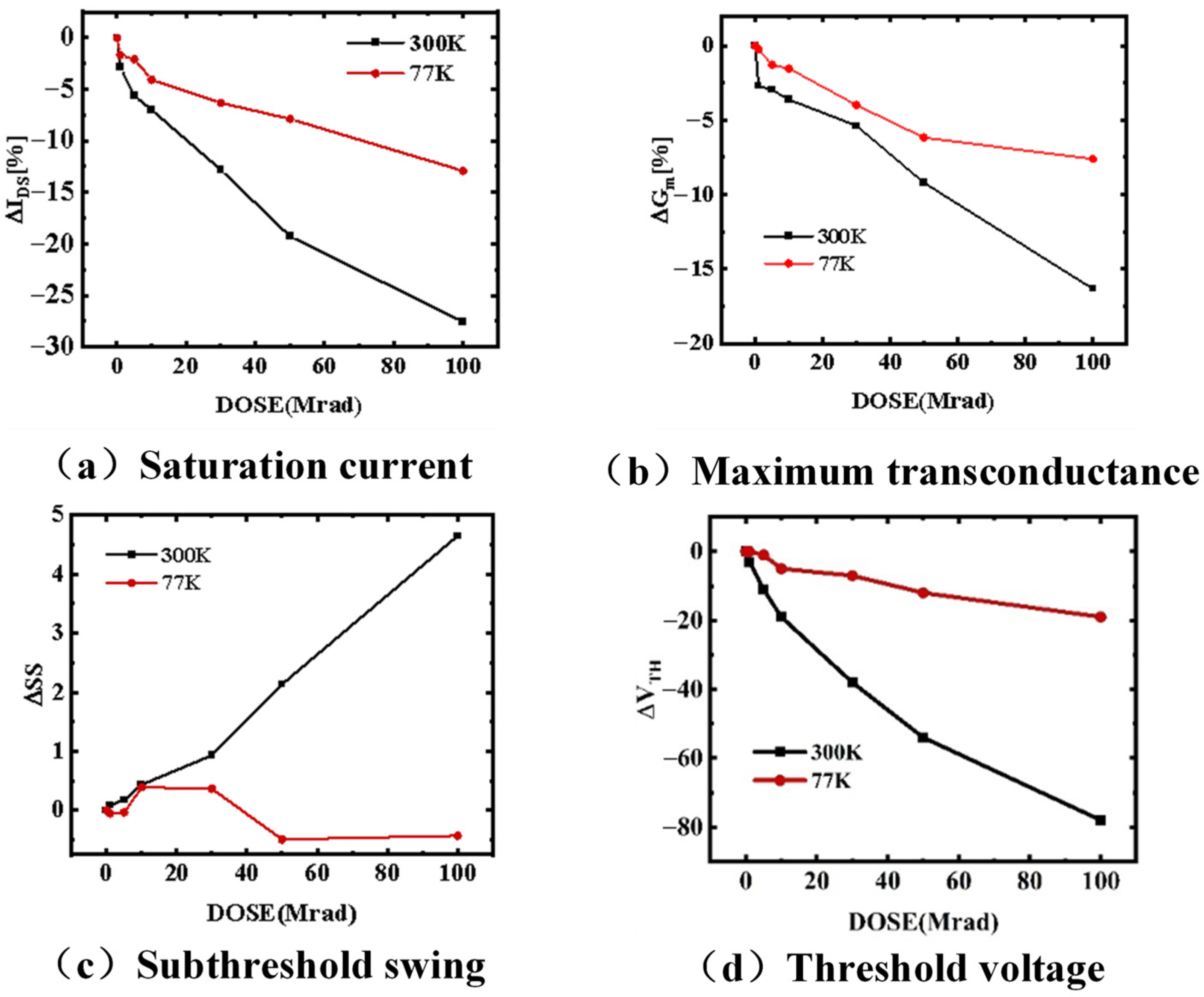
Figure 3 shows the degradation characteristics of FinFETs under different total ionizing dose (TID) radiation conditions at 300 K (room temperature) and 77 K (low temperature). From the experimental results, it can be observed that after radiation, the threshold voltage degrades by 80 mV at room temperature, while the degradation is only 20 mV at low temperature. At room temperature, the saturated current and transconductance decrease by 30% and 17%, respectively, after radiation, whereas the degradation of these two parameters under low-temperature radiation is approximately half of that at room temperature. Regardless of radiation at room temperature or low temperature, the threshold voltage, saturated current, and transconductance of the device exhibit a saturation trend with the increase in TID.
Based on the analysis, the ultra-thin gate oxide layer of FinFETs is insensitive to the TID effect. The TID degradation mechanism of FinFETs irradiated at ultra-high doses is dominated by charge trapping in the shallow trench isolation (STI) region and interface states at the STI/SiO2 interface. Electron–hole pairs generated by TID radiation are separated under the action of an electric field: electrons are quickly swept out of the oxide layer, while a portion of electron–hole pairs undergo initial recombination. The probability of initial recombination is related to the oxide electric field, radiation particle type, and temperature. The escape probability of electron–hole pairs at 77 K is much lower than that at 300 K, indicating that radiation-induced trapped charges are significantly reduced at low temperatures, which explains why the radiation-induced degradation of devices at low temperatures is smaller than that at room temperature.
At 300 K, the TID response is affected by oxide charges in the STI region and acceptor-like interface states at the STI/Si and gate oxide/Si interfaces. At 77 K, the TID response is dominated by positive oxide charges in the STI region. This is mainly because most electron–hole pairs generated by radiation at room temperature recombine, and the remaining electrons are quickly swept out of the oxide layer. In contrast, the mobility of holes is relatively low, leading to their accumulation in the oxide layer and the formation of positive oxide trapped charges. At low temperatures, however, the generated holes are trapped near their generation sites—most holes are captured by nearby defects before recombination can occur. Consequently, the device degradation after low-temperature radiation is mainly affected by trapped charges in the STI region. Meanwhile, the generation of interface states is suppressed at low temperatures. Therefore, the positive oxide charges in the STI region induce carrier inversion in the channel area adjacent to the STI, forming a source-drain parasitic path. This results in early turn-on of the device and an increase in off-state current.
4. Simulation Results and Analysis
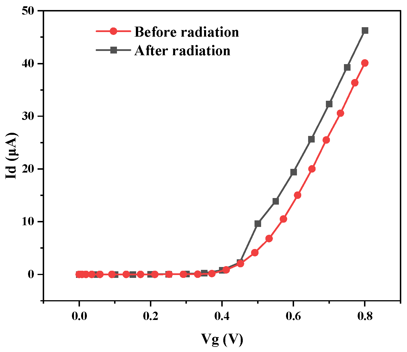
Figure 4 shows the changes in the Id-Vg characteristic curves of the established FinFET device model before and after total dose radiation. It can be observed that the characteristic curves shift negatively after total dose radiation. Under the same gate voltage, the drain current increases significantly after radiation. The analysis suggests that this is due to the trap charges generated in the oxide layer by total dose radiation. For FinFETs, their unique three-dimensional structure causes the source and drain to be surrounded by gate oxide on three sides, resulting in more trap charges at the interface. Under the same gate voltage, there are more electron–hole pairs near the channel, thus leading to a higher drain current.
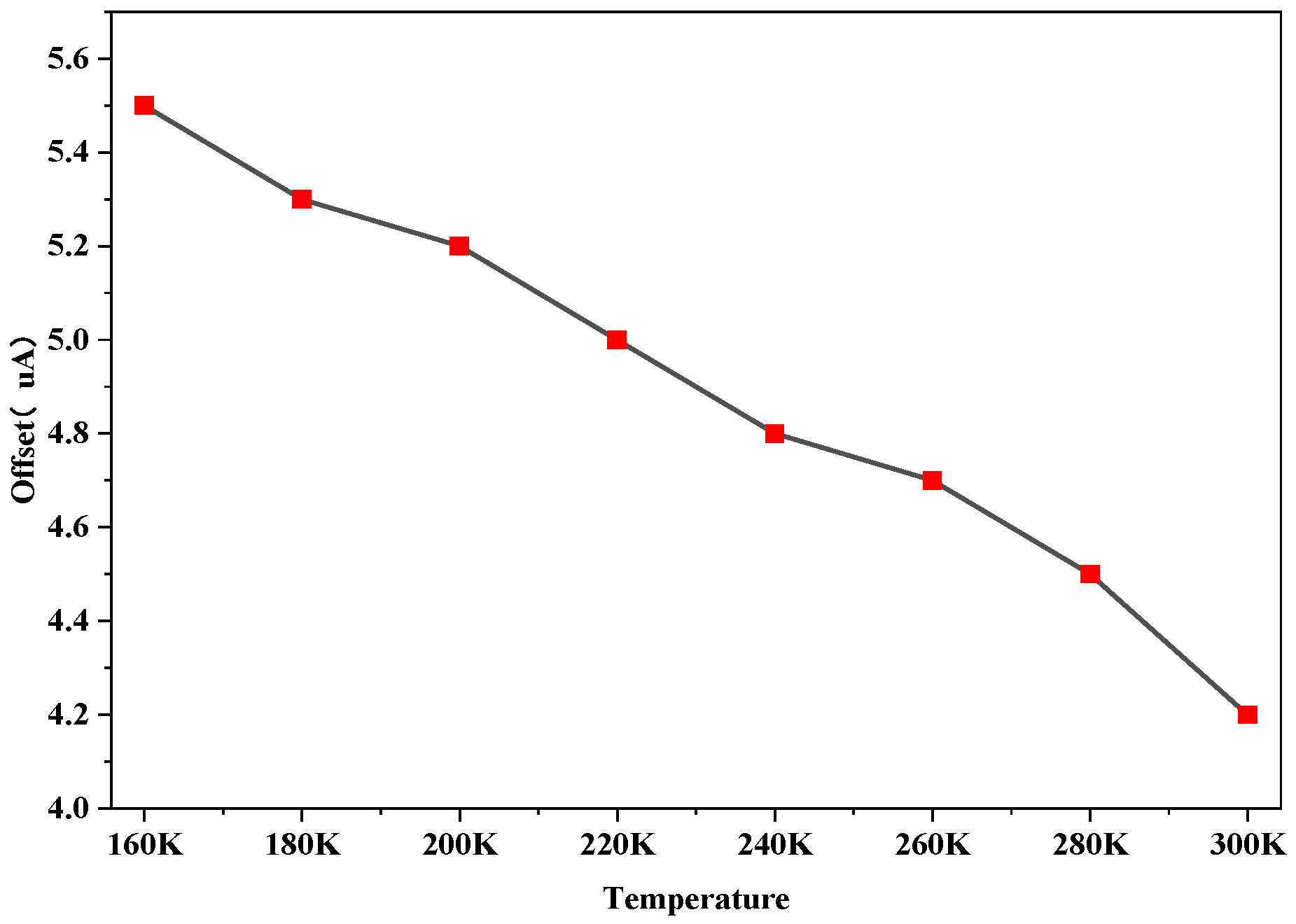
Figure 5 shows a comparison of the drain current offset of FinFETs before and after total dose radiation at different temperatures. It can be seen that as the temperature decreases, the offset gradually increases, showing an approximately linear relationship. An increase in Id allows the device to have a larger bandwidth under the same power consumption, but it also leads to higher device power consumption. The mobility μ shows a linear increasing trend as the temperature decreases; with decreasing temperature, the mobility μ increases by 975 cm
2/(V·s). Carrier mobility μ is composed of Coulomb scattering, surface roughness scattering, and phonon scattering. In bulk silicon technology, the temperature dependence of phonon scattering is approximately μ~T
−3/
2. Fewer phonon scatterings can enhance μ at low temperatures. Improved mobility means that carriers can achieve a higher drift velocity under the same electric field strength; thus, under the same bias conditions, MOS transistors can provide a larger drive current, enhancing their driving capability.
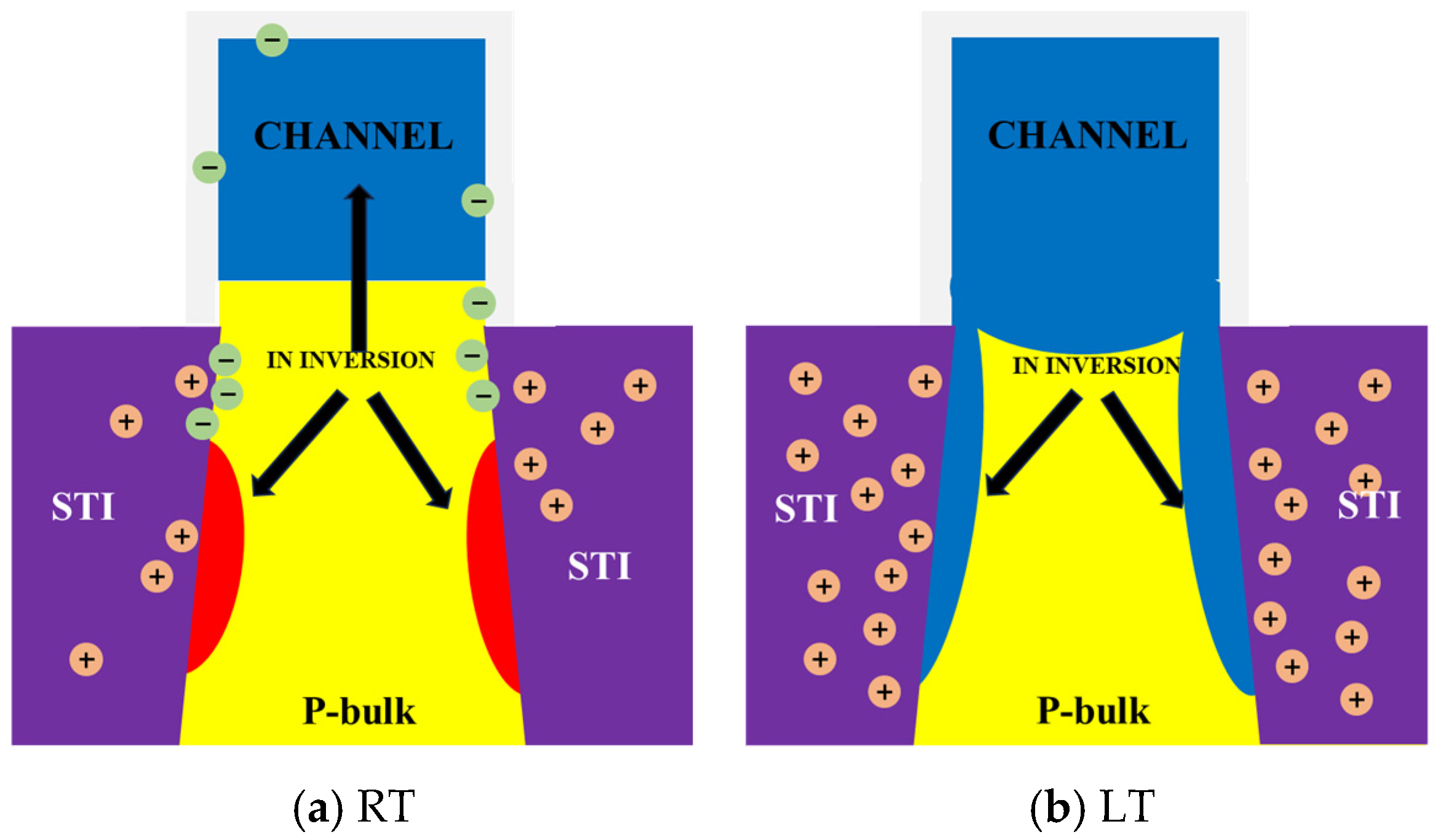
Analysis of simulation results reveals that, under 300 K conditions, the total dose radiation response of the device is co-dominated by oxide charges within the shallow trench isolation (STI) structure and acceptor-type interface states formed at both the STI/Si and gate oxide/Si interfaces. As shown in
Figure 6. Notably, STI serves as the core isolation structure for adjacent active regions in FinFET devices: under irradiation, its internal oxide layer generates oxide charges dominated by hole trapping—comprising positive charges and a small fraction of negative charges arising from electron trapping. The acceptor-type interface states at the STI/Si and gate oxide/Si interfaces are essentially trap energy levels originating from defects (e.g., dangling bonds, oxygen vacancies) induced by radiation-induced lattice disruption. These charges and interface states directly induce degradation of key electrical parameters (e.g., threshold voltage drift, leakage current elevation) by modifying the device’s internal electric field distribution, obstructing carrier transport pathways, and increasing carrier recombination centers—thereby collectively governing the overall Total Ionizing Dose (TID) response characteristics at room temperature.
As shown in
Figure 7. In a low-temperature irradiation environment, the dominant factor governing TID response shifts significantly: positive oxide charges in STI emerge as the core regulatory factor of the TID effect. This phenomenon is inherently linked to the dynamic behavior of carriers under low-temperature conditions. At low temperatures, hole mobility is substantially reduced due to temperature dependence, resulting in a marked decrease in their migration rate. Furthermore, the inadequate thermal activation energy available at low temperatures means that once holes are trapped by defect centers (e.g., oxygen vacancies, silicon dangling bonds) in the STI oxide layer, they can barely escape the trap sites for long-range migration—effectively being “fixed” near their generation sources to form localized positive charge accumulation regions. Simultaneously, the low-temperature environment markedly enhances the probability of secondary recombination of holes in both the STI/Si substrate interface recombination region and the defect-rich regions within the oxide layer. Their prolonged retention time facilitates recombination with electrons generated by subsequent irradiation, reducing the number of effective carriers available for charge transport or trapping—thereby accelerating the accumulation rate of positive charges in STI.
This rapid accumulation of positive charges rapidly screens the ionizing electric field induced by irradiation, lowering the efficiency of subsequent charge trapping. Consequently, the device’s TID response exhibits a distinct saturation trend at a relatively low total radiation dose—forming a stark contrast to the slow saturation behavior observed at room temperature, which is dominated by the dynamic balance of charge migration and recombination.
5. Conclusions
This paper focuses on the low-temperature total dose radiation effects of FinFET transistors. Experimental measurements were conducted to obtain the total ionizing dose (TID) radiation degradation characteristics of FinFET devices under room temperature (300 K) and low temperature (77 K) conditions. With the help of TCAD simulation technology, it reveals the degradation laws of devices after radiation and theoretically analyzes the electronic properties, formation, and evolution mechanisms of radiation-induced defects in low-temperature environments. On this basis, a physical model for the low-temperature total dose effects of FinFET transistors is established. This model can provide direct theoretical support for the radiation hardening design of FinFET devices and lay a technical foundation for their reliable application in extreme low-temperature radiation environments (such as space). In the future, device structures and process parameters can be further optimized based on this model to expand its application potential in a wider range of extreme scenarios.
Author Contributions
Conceptualization, C.L. and Q.Z.; methodology, Q.Z.; software, Q.Z.; validation, J.Z., L.G. and Y.X.; formal analysis, Q.Z.; investigation, Y.X.; resources, J.Z.; data curation, L.G.; writing—original draft preparation, Q.Z.; writing—review and editing, Q.Z.; visualization, Y.X.; supervision, C.L.; project administration, M.H. and C.L. All authors have read and agreed to the published version of the manuscript.
Funding
This research was funded by General Project of National Defense Science and Technology Key Laboratory Fund, grant number 6142806230204.
Data Availability Statement
The original contributions presented in this study are included in the article. Further inquiries can be directed to the corresponding author.
Conflicts of Interest
The authors declare no conflict of interest.
References
- Aghanim, N.; Akrami, Y.; Ashdown, M.; Aumont, J.; Baccigalupi, C.; Ballardini, M.; Banday, A.; Barreiro, R.; Bartolo, N.; Basak, S.; et al. Planck 2018 Results. VI. Cosmological Parameters. Astron. Astrophys. 2020, 641, A6. [Google Scholar] [CrossRef]
- MRO/MCS Team. Mars Climate Sounder (MCS) Temperature Profiles[R/OL]; Planetary Data System (PDS) Atmospheres Node: Boulder, CO, USA, 2025. [Google Scholar]
- Jungsik, N.; Chang, Y.K.; Kwang, P.K. Influence of Ionizing Radiation on Short-Channel Effects in Low-Doped Multi-Gate MOSFETs. IEEE Trans. Nucl. Sci. 2012, 59, 3021–3026. [Google Scholar] [CrossRef]
- Hu, Z.Y.; Liu, Z.L.; Hua, S.; Zhang, Z.; Ning, B.; Chen, M.; Bi, D.; Zou, S. Radiation Hardening by Applying Substrate Bias. IEEE Trans. Nucl. Sci. 2011, 58, 1355–1360. [Google Scholar] [CrossRef]
- Chatterjee, I.; Zhang, E.X.; Bhuva, B.L.; Reed, R.A.; Alles, M.L.; Mahatme, N.N.; Ball, D.R.; Schrimpf, R.D.; Fleetwood, D.M.; Linten, D.; et al. Geometry Dependence of Total-Dose Effects in Bulk FinFETs. IEEE Trans. Nucl. Sci. 2014, 61, 2951–2958. [Google Scholar] [CrossRef]
- Chatterjee, I.; Zhang, E.X.; Bhuva, B.L.; Alles, M.A.; Schrimpf, R.D.; Fleetwood, D.M.; Fang, Y.-P.; Oates, A. Bias Dependence of Total-Dose Effects in Bulk FinFETs. IEEE Trans. Nucl. Sci. 2013, 60, 4476–4482. [Google Scholar] [CrossRef]
- Ma, T.; Dressendorfer, P. Ionizing Radiation Effects in MOS Devices and Circuits; Wiley: New York, NY, USA, 1989; pp. 172–173. [Google Scholar]
- Boesch, H.; McGarrity, J. Charge Yield and Dose Effects in MOS Capacitors at 80K. IEEE Trans. Nucl. Sci. 1976, 23, 1520–1525. [Google Scholar] [CrossRef]
- Saks, N.S.; Ancona, M.G. Generation of Interface States by Ionizing Radiation at 80K Measured by Charge Pumping and Subthreshold Slope Techniques. IEEE Trans. Nucl. Sci. 1987, 34, 1347–1354. [Google Scholar] [CrossRef]
- Winokur, P.S.; Boesch, H.E. Interface-State Generation in Radiation-Hard Oxides. IEEE Trans. Nucl. Sci. 1980, 27, 1647–1650. [Google Scholar] [CrossRef]
- Freitag, R.K.; Burke, E.A.; Dozier, C.M.; Brown, D. The Development of Non-Uniform Deposition of Holes in Gate Oxides. IEEE Trans. Nucl. Sci. 1988, 35, 1203–1207. [Google Scholar] [CrossRef]
- El-Mamouni, F.; Zhang, E.X.; Ball, D.R.; Sierawski, B.; King, M.P.; Schrimpf, R.D.; Reed, R.A.; Alles, M.L.; Fleetwood, D.M.; Linten, D.; et al. Heavy-Ion-Induced Current Transients in Bulk and SOI FinFETs. IEEE Trans. Nucl. Sci. 2012, 59, 2674–2681. [Google Scholar] [CrossRef]
- Chiarella, T.; Witters, L.; Mercha, A.; Kerner, C.; Rakowski, M.; Ortolland, C.; Ragnarsson, L.-Å.; Parvais, B.; De Keersgieter, A.; Kubicek, S.; et al. Benchmarking SOI and Bulk FinFET Alternatives for Planar CMOS Scaling Succession. Solid-State Electron. 2010, 54, 855–860. [Google Scholar] [CrossRef]
- Jacoboni, C.; Canali, C.; Ottaviani, G.; Quaranta, A.A. A Review of Some Charge Transport Properties of Silicon. Solid-State Electron. 1977, 20, 77–89. [Google Scholar] [CrossRef]
- Ortiz-Conde, A.; Garcia-Sanchez, F.; Liou, J.J.; Cerdeira, A.; Estrada, M.; Yue, Y. A Review of Recent MOSFET Threshold Voltage Extraction Methods. Microelectron. Reliab. 2002, 42, 583–596. [Google Scholar] [CrossRef]
- Chen, H.H.; Gong, J. The Temperature-Dependence of Threshold Voltage of N-MOSFETs with Nonuniform Substrate Doping. Solid-State Electron. 1998, 42, 1799–1805. [Google Scholar] [CrossRef]
- Goel, N.; Tripathi, A. Temperature Effects on Threshold Voltage and Mobility for Partially Depleted SOI MOSFET. Int. J. Comput. Appl. 2012, 42, 56–58. [Google Scholar]
- Bongim, J.; Diestelhorst, R.M.; Bellini, M.; Espinel, G.; Appaswamy, A.; Prakash, A.G.; Cressler, J.D.; Chen, D.; Schrimpf, R.D.; Fleetwood, D.M.; et al. Temperature-Dependence of Off-State Drain Leakage in X-Ray Irradiated 130 nm CMOS Devices. IEEE Trans. Nucl. Sci. 2006, 53, 3203–3209. [Google Scholar]
- Subramanian, V.; Bhattacharya, P.K. The Effect of Ionizing Radiation Damage on the Transconductance of Short Channel Insulated Gate Field Effect Transistors. Jpn. J. Appl. Phys. 1995, 34, 1809–1815. [Google Scholar] [CrossRef]
- Kuznetsov, V.; Andreev, D.; Andreev, V.; Piskunov, S.; Popov, A.I. The Compact Model Synthesis for the RADFET Device. Technologies 2025, 13, 492. [Google Scholar] [CrossRef]
- Karimi, K.; Fardoost, A.; Javanmard, M. Comprehensive review of finfet technology: History, structure, challenges, innovations, and emerging sensing applications. Micromachines 2024, 15, 1187. [Google Scholar] [CrossRef]
- Johnston, A.H.; Swimm, R.T.; Thorbourn, D.O. Charge yield at low electric fields: Considerations for bipolar integrated circuits. IEEE Trans. Nucl. Sci. 2013, 60, 4488–4497. [Google Scholar] [CrossRef]
- Feng, Y.; Guo, H.; Ma, W.; Hu, J.; Ouyang, X.; Zhang, J.; Zhang, F.; Zhang, H.; Bai, R.; Ma, X.; et al. Effect of 60Coγ ray radiation on electrical properties of SiGe HBTs at low temperatures. Microelectron. J. 2024, 144, 106058. [Google Scholar] [CrossRef]
| Disclaimer/Publisher’s Note: The statements, opinions and data contained in all publications are solely those of the individual author(s) and contributor(s) and not of MDPI and/or the editor(s). MDPI and/or the editor(s) disclaim responsibility for any injury to people or property resulting from any ideas, methods, instructions or products referred to in the content. |
© 2025 by the authors. Licensee MDPI, Basel, Switzerland. This article is an open access article distributed under the terms and conditions of the Creative Commons Attribution (CC BY) license (https://creativecommons.org/licenses/by/4.0/).


