Abstract
This paper presents the electrical characterization of the on-resistance (RON) of on-wafer 100 V p-GaN power High-Electron-Mobility Transistors (HEMTs). This study assesses device degradation in the context of a monolithically integrated half-bridge circuit, considering both Low-Side (LS) and High-Side (HS) configurations. Since on-wafer samples have been characterized, a custom experimental setup was developed to emulate stress conditions experienced by the devices in the half-bridge circuit. A periodic signal (T = 10 µs, TON = 2 µs) switching from the OFF to the ON state was applied for a cumulative duration of 1000 s. Different OFF-state stress conditions were applied by varying the gate-source OFF voltage (VGS,OFF) between 0 V and −10 V. The on-resistance exhibited a positive drift over time for devices in either the LS or the HS configuration, with the latter showing a more pronounced degradation. Measurements at higher temperatures (up to 90 °C) were carried out to characterize the dynamics of the physical mechanism behind the degradation effects. We identified hole emission from C-related acceptor traps in the buffer as the main mechanism for the observed degradation, which is present in both the HS and the LS configurations. The additional degradation observed in the HS case was attributed to the back-gating effect, stemming from the non-null body-to-source voltage. Furthermore, we found that a more negative VGS,OFF further increases RON degradation, likely related to the higher electric field near the gate contact, which enhances hole emission from C-related acceptor traps.
1. Introduction
Gallium Nitride (GaN) High-Electron-Mobility Transistor (HEMT) is leading the next generation of power switches due to its high frequency and high power capability [1]. More specifically, GaN-on-Si is a particularly interesting platform thanks to its potential for monolithic integration [2]. Despite already being commercialized, GaN-on-Si power devices are still far from reaching their maximum theoretical performance due to, amongst other things, trapping effects occurring during device operation [3]. So far, device-level characterization has been extensively conducted, allowing for a deep understanding of how the trapping mechanisms work in this type of device [4,5,6,7,8,9,10,11,12,13,14]. However, trap dynamics characterization under realistic circuit operating conditions is far less investigated. For example, in monolithically integrated half-bridge circuits, the High side (HS) and Low Side (LS) devices experience different degradation levels in terms of both on-resistance (RON) and threshold voltage (VTH), due to the non-null source-to-body voltage present in HS devices [15,16]. The goal of this paper is to analyze the effect of OFF-state stress on the device performance from the trapping point of view. We find that the core mechanism causing the dispersion of device performance is the hole emission from C-related acceptor traps inside the buffer layer. This mechanism is common for both HS and LS. The additional degradation experienced by the HS device is explained as being due to a purely electrostatic phenomenon due to the so-called back-gating effect. This conclusion is further confirmed by the fact that the time constants and the activation energies (EAs) extracted from the HS and LS transient are essentially the same. Moreover, we find that the negative OFF-state gate voltage enhances the degradation caused by the high drain voltage, and this effect can be explained with the accumulation of negative charges in the AlGaN barrier, which deplete the 2-DEG (two-dimensional electron gas), thus increasing the magnitude of the observed dispersion [17,18].
2. Experimental Setup
Figure 1 shows the cross-section of the DUT, which is a 100 V p-GaN HEMT. LG is lower than 1 µm and LGD is lower than 3 µm, allowing a relatively low voltage range of operation (for comparison, the 650 V p-GaN technology typically involves an LGD longer than 15 µm). As customary for GaN power HEMTs, the buffer is C-doped to obtain a semi-insulating layer with a C concentration between 5 × 10¹⁸ and 5 × 10¹⁹. The p-GaN region in the gate stack is used to deplete 2-DEG under the gate at VGS = 0 V and thus achieve normally off operation, i.e., VTH > 0 V. The circuit employed for the electrical characterization is shown in Figure 2. The drain voltage is supplied by a pair of isolated DC/DC converters that can generate a 50 V isolated voltage. The bulk of the device is connected either to the ground or to the negative terminal of VD to emulate, respectively, the LS and HS configurations. The only difference between LS and HS is the source-to-body voltage, which is 0 V for the LS, while in HS, a non-null VSB is present. This mimics the additional voltage stress experienced by the High-Side device of an integrated half-bridge structure. To improve the Digital Store Oscilloscope (DSO) resolution, we use the clamping circuit shown in Figure 2b. The clamping circuit allows VDS to be measured in its rise as long as VDS < VZ. When VDS reaches the level set by the Zener diode (~4 V), diodes D1 and D2 start to conduct and prevent VDS from rising further. Effectively, the circuit clamps the maximum level of VDS measured by the DSO [19]. This circuit is required only to improve the resolution of the voltage signal measured by the DSO, while the DUT experiences the full 50 V signal as set by the DC/DC converters.
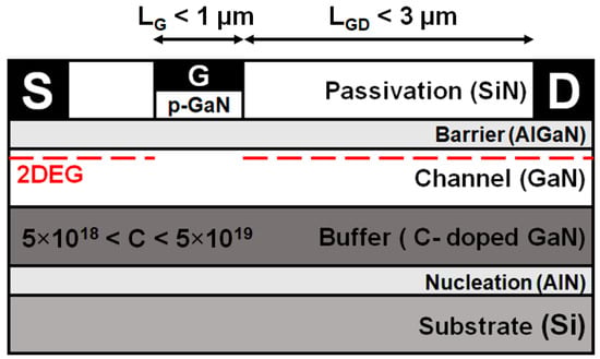
Figure 1.
Schematic view of the cross-section of the DUT. The p-GaN under the gate creates an effective ‘p-i-n’ junction towards the source, which depletes the 2DEG at VGS = 0 V and thus allows a normally off operation (i.e., VT > 0 V). The gate–drain distance is such that the 100 V range operation can be withstood, and the carbon concentration in the buffer layer is between 5 × 10¹⁸ and 5 × 10¹⁹ to obtain a semi-insulating layer.
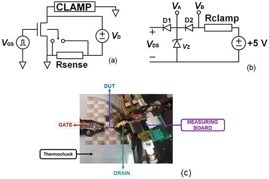
Figure 2.
The measuring board (a) used for the measurement, VD, is provided by means of DC/DC isolated converters. The switch is connected either to the ground (LS) or to the negative pin of the VD (HS). The clamping circuit (b) is used to block the rise in the VDS for a more precise measure with the DSO. We calculate the real VDS,ON with the voltages VA and VB (). In panel (c), a picture of the measurement setup used in this paper is shown for reference.
The typical DC output (ID-VDS) and transfer (ID,IG-VGS) characteristic are shown in Figure 3. From these curves, we can extract the threshold voltage and the static on-resistance, which are, respectively, VTH ≈ 2 V and RON ≈ 20 Ω. More details on the contact resistance and the device structure can be found in [20].
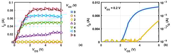
Figure 3.
Typical output (a) and transfer (b) DC characteristics of the DUT. From these measurements, we can extract the static value of the on-resistance (RON ≈ 20 Ω) and the threshold voltage (VTH ≈ 2 V), respectively.
The gate of the DUT is driven with a pulsed signal from a waveform generator that switches the device between VGS,ON (6 V) and VGS,OFF (0; −2; −5; −8; −10 V). The drain voltage applied to the device is VDS = 50 V during the OFF state and ~200 mV during the ON state. VDS,OFF has been chosen as 50 V to ensure a test condition comparable with the real application of GaN HEMTs (e.g., 48 V DC/DC converter). The switching period is T = 10 µs with TON = 2 µs. The RON measure is performed by extracting the current during the ON state. The total time taken by the experiment is 1000 s. Before the beginning of each measurement, the DUT is biased in the ON state with low VDS (~200 mV) and VSB = 0 V for 100 s to guarantee a common stress-free initial condition for both the LS and HS configurations. Figure 4 shows the first period of the stress cycle to illustrate the setup.
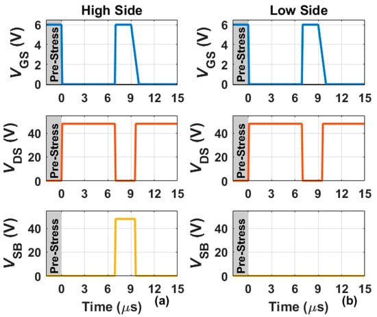
Figure 4.
The first waveform of the stress period. In LS (b), the VDS switch between high and low according to the value of the VGS and the VSB is always zero, regardless of the device condition. In HS (a), the VDS behaves like in LS, but the VSB goes high during the TON, giving an additional stress component.
3. Experimental Results
Figure 5 shows the normalized dynamic on-resistance (RON/RON,0) for VGS,OFF varying from 0 V to −10 V for both LS and HS. RON,0 is taken as the measurement of the first stress pulse. The baseplate temperature for this experiment was set to 60 °C. We can see that for both HS and LS configurations, increasing the negative VGS,OFF causes an increased magnitude of degradation. More specifically, degradation increases from ~20% at 0 V to ~55% at −10 V (LS) and from ~65% at 0 V to ~120% at −10 V (HS). Interestingly, we find that while the OFF-state gate voltage has a significant effect on the magnitude of degradation, it does not appear to have significant effect on the time constant of the transient. This is discussed further when presenting the data at different temperatures.
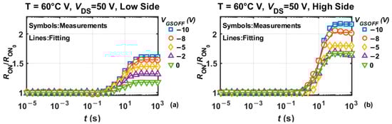
Figure 5.
The transient for different VGS,OFF in LS (a) and HS (b). A higher OFF-state gate voltage (in absolute value) increases the degradation from the device. While the OFF-state gate voltage has a strong effect on the magnitude of the degradation, it appears to have no significant effect on the time constant of the transient.
Stress measurements have been carried out at different temperatures (60 °C to 90 °C with ΔT = 10 °C) for each of the VGS,OFF (from 0 V to −10 V). Figure 6 shows the transients under the different conditions for the LS device. As can be seen, for VGS,OFF = 0 V, the maximum degradation increases from ~17% at 60 °C to 28% at 90 °C. It is noticeable that the increasing temperature not only has the effect of increasing the amplitude of the dynamic on-resistance but also to accelerates it. Figure 7 shows the results of the characterization on the HS device. Similar considerations as those observed for the LS device can be drawn, with the main difference being the increased degradation of the HS device. The degradation at VGS,OFF = 0 V increases from ~65% (at 60 °C) to ~80% (at 90 °C). The temperature accelerates the transient in a manner similar to what occurs in the LS configuration. Figure 8 shows the Arrhenius plot constructed by using the time constants (τ) extracted from the temperature transients, and the exact values of the τs can be found in Table 1 and Table 2. It can be seen how the extract τs for HS and LS at each VGS,OFF are essentially the same, indicating that the main mechanism responsible for the degradation is the same, specifically hole emission from the CN state in the buffer. In Figure 9, the dynamic has been normalized between 0 and 1 to highlight the independence of the time constant from the conditions (LS or HS) and the OFF-state gate voltage applied. As observed in our previous works [4,21], hole emission increases the negative charge due to ionized acceptor traps in the buffer, thus reducing the 2-DEG concentration. The activation energy extracted (0.53 eV) is slightly lower to the one normally extracted for the C-related acceptor traps inside the buffer layer, i.e., 0.9 eV above the valence band [22,23,24,25,26]. However, it might be possible that field enhancement mechanisms such as the Poole–Frenkel effect, which cause a lowering of the energy barrier for carrier emission at high VDS voltages, explain the lower EAs extracted from the data [22,27,28].
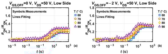
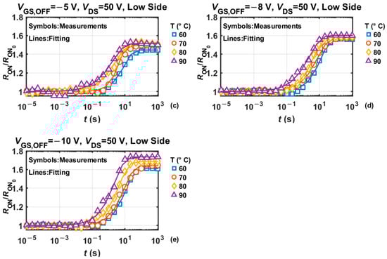
Figure 6.
Temperature transient for VGS,OFF varying from 0 to −10 (a–e) for LS configuration. We can observe that regardless of the OFF-state gate voltage applied, the increasing temperature enhances the magnitude of the degradation and accelerates it.
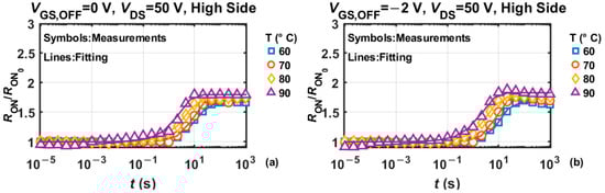
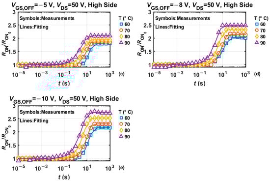
Figure 7.
Temperature transient for VGS,OFF varying from 0 to −10 (a–e) for HS configuration. We can observe that regardless of the OFF-state gate voltage applied, the increasing temperature enhances the magnitude of the degradation and accelerates it.
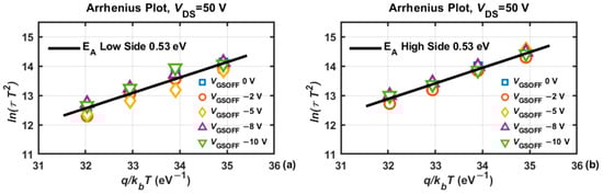
Figure 8.
Arrhenius plot extracted from the time constant (τ) of the transient at different temperatures and VGS,OFF. We can see that both LS (a) and HS (b) are comparable in terms of τ and activation energy. This means that the root cause for the degradation in both cases is the same (i.e., CN states inside buffer layer).

Table 1.
Time constant for LS measurements.
Table 2.
Time constant for HS measurements.
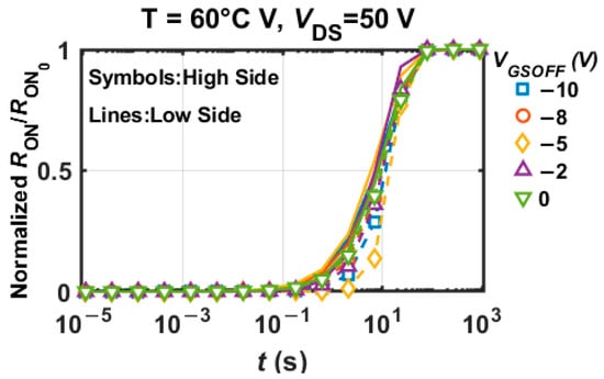
Figure 9.
Dynamic on-resistance normalized between 0 and 1 for a baseplate temperature of 60 °C. This graph clearly shows the independence of the dynamic from the condition (LS and HS) and from the OFF-state gate voltage.
The increased magnitude of the degradation in HS can be attributed to the back-gating effect, which is present when the substrate and the source are at a different potential [29]. Under this condition, the 2-DEG is more depleted compared to the condition where VSB = 0 due to the higher relative shift between EC and EF. Moreover, the negative substrate potential promotes the hole emission from CN states, resulting in a larger amplitude of the RON dynamic. Nevertheless, the dynamics governed by the trapping process are the same for both LS and HS devices [16,22,30,31].
Concerning the increase in degradation magnitude observed when a negative VGS,OFF is applied, this could be attributed to the enhancing of the vertical electric field under the gate during the OFF state. The band bending induced by the field enhances the hole emission from the C-related acceptor traps located inside the buffer layer. As a consequence, a higher number of holes are emitted from such traps; this results in a buffer layer that becomes even more negatively charged with respect to the condition with VGS,OFF = 0, resulting in a stronger depletion of the 2DEG and thus a higher amplitude of the dynamic on-resistance. In Figure 10a, a sketch of the energy band illustrates this point.
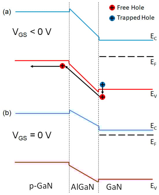
Figure 10.
Sketch of the energy band in OFF-state when the VGS is lower than 0 (a). When the negative VGS is applied, the vertical field applied promotes the hole emission from the C-related acceptor traps inside the buffer, which are attracted by the negative potential applied to the gate contact. In panel (b), the equilibrium condition is shown as a reference.
4. Conclusions
In this paper, we have characterized the dynamic on-resistance of on-wafer 100 V p-GaN HEMTs by means of a custom measurement setup able to replicate Low- and High-Side biasing conditions of devices to be employed in monolithically integrated half-bridge circuits. In particular, this setup allows for considering the non-null source-to-body voltage experienced by the HS device during operation. The root cause for RON degradation in both LS and HS is found to be the hole emission from CN states inside the buffer layer, as confirmed by the extracted activation energies, which are compatible with C-related acceptor traps. The additional degradation experienced by the device in HS (with respect to the LS case) is due to the negative bias applied between the substrate and the source, which causes an electrostatic back-gating effect. Finally, it was found that increasing the magnitude of the negative gate voltage applied during OFF-state stress further increases dynamic RON, in both LS and HS cases. This was attributed to the higher electric field near the gate contact, which enhances hole emission from C-related acceptor traps, thus leading to a larger dynamic RON variation.
Author Contributions
Conceptualization, L.M. and A.C.; Methodology, L.M. and A.C.; Software, L.M.; Validation, L.M.; Formal analysis, L.M.; Investigation, L.M. and N.Z.; Resources, L.M. and A.C.; Data curation, L.M.; Writing—original draft, L.M.; Writing—review & editing, N.Z., M.C., G.C., G.G., F.I., G.V. and A.C.; Visualization, L.M.; Supervision, N.Z. and A.C.; Project administration, A.C.; Funding acquisition, A.C. All authors have read and agreed to the published version of the manuscript.
Funding
This work has been funded by the European Union–NextGenerationEU, within the framework of the National Recovery and Resilience Plan (NRRP), Mission 4 Component 2 Investment 1.4-Call for tender n. 3138/2021 modified by the Directorial Decree n. 3175/2021 of the Italian Ministry of University and Research (MUR), Project Code CN00000023, Concession Decree n. 0001033 adopted by the Italian Ministry of University and Research (MUR) on 17 June 2022, CUP E93C22001070001, Project title “Sustainable Mobility Center (CNMS)”.
Data Availability Statement
Data are contained within the article.
Acknowledgments
The views and opinions expressed are those of the authors only and do not necessarily reflect those of the European Union or the European Commission. Neither the European Union nor the European Commission can be held responsible for them.
Conflicts of Interest
Authors Marcello Cioni, Giacomo Cappellini, Giovanni Giorgino and Ferdinando Iucolano were employed by the company STMicroelectronics. The remaining authors declare that the research was conducted in the absence of any commercial or financial relationships that could be construed as a potential conflict of interest.
References
- Udabe, A.; Baraia-Etxaburu, I.; Diez, D.G. Gallium Nitride Power Devices: A State of the Art Review. IEEE Access 2023, 11, 48628–48650. [Google Scholar] [CrossRef]
- Wei, J.; Zheng, Z.; Tang, G.; Xu, H.; Lyu, G.; Zhang, L.; Chen, J.; Hua, M.; Feng, S.; Chen, T.; et al. GaN Power Integration Technology and Its Future Prospects. IEEE Trans. Electron. Devices 2023, 71, 1365–1382. [Google Scholar] [CrossRef]
- Lee, Y.-H.; Chen, P.-H.; Zhang, Y.-C.; Wu, C.-W.; Chou, S.-Y.; Wang, Y.-B.; Kuo, H.-M.; Lin, Y.-S.; Chen, Y.-T.; Tsai, Y.-J.; et al. An Approach to Extract the Trap States via the Dynamic Ron Method with Substrate Voltage Applied During the Recovery Time. IEEE Trans. Electron. Devices 2024, 71, 6616–6619. [Google Scholar] [CrossRef]
- Zagni, N.; Chini, A.; Puglisi, F.M.; Meneghini, M.; Meneghesso, G.; Zanoni, E.; Pavan, P.; Verzellesi, G. “Hole Redistribution” Model Explaining the Thermally Activated RON Stress/Recovery Transients in Carbon-Doped AlGaN/GaN Power MIS-HEMTs. IEEE Trans. Electron. Devices 2021, 68, 697–703. [Google Scholar] [CrossRef]
- Li, S.; Yang, S.; Han, S.; Sheng, K. Investigation of Temperature-Dependent Dynamic RON of GaN HEMT with Hybrid-Drain under Hard and Soft Switching. In Proceedings of the 2020 32nd International Symposium on Power Semiconductor Devices and ICs (ISPSD), Vienna, Austria, 13–18 September 2020; IEEE: New York, NY, USA, 2020; pp. 306–309. [Google Scholar]
- Chiu, H.-C.; Peng, L.-Y.; Yang, C.-W.; Wang, H.-C.; Hsin, Y.-M.; Chyi, J.-I. Analysis of the Back-Gate Effect in Normally OFF p-GaN Gate High-Electron Mobility Transistor. IEEE Trans. Electron. Devices 2015, 62, 507–511. [Google Scholar] [CrossRef]
- Li, S.; Sheng, K.; Yang, S. Temperature-Dependent Dynamic Ron of GaN E-HEMTs: The Impact of p-GaN Drain. IEEE Trans. Electron. Devices 2023, 70, 3754–3761. [Google Scholar] [CrossRef]
- Meneghini, M.; Vanmeerbeek, P.; Silvestri, R.; Dalcanale, S.; Banerjee, A.; Bisi, D.; Zanoni, E.; Meneghesso, G.; Moens, P. Temperature-Dependent Dynamic RON in GaN-Based MIS-HEMTs: Role of Surface Traps and Buffer Leakage. IEEE Trans. Electron. Devices 2015, 62, 782–787. [Google Scholar] [CrossRef]
- Boito, M.; Fregolent, M.; De Santi, C.; Abbisogni, A.; Smerzi, S.; Rossetto, I.; Iucolano, F.; Meneghesso, G.; Zanoni, E.; Meneghini, M. On-Wafer Dynamic Operation of Power GaN-HEMTs: Degradation Processes Investigated by a Novel Experimental Approach. In Proceedings of the 2024 IEEE International Reliability Physics Symposium (IRPS), Grapevine, TX, USA, 14–18 April 2024; IEEE: New York, NY, USA, 2024; pp. 1–5. [Google Scholar]
- Chen, Y.-H.; Chou, S.-Y.; Chen, M.-C.; Chang, T.-C.; Wang, Y.-B.; Zhang, Y.-C.; Wu, C.-W.; Lin, C.-H.; Hsu, J.-T.; Lee, Y.-H.; et al. Study of Vth Instability During Recovery After Off-State Stress in p-GaN HEMT. IEEE Electron. Device Lett. 2025, 46, 1717–1720. [Google Scholar] [CrossRef]
- Yeh, C.-H.; Chen, P.-H.; Chang, T.-C.; Chang, K.-C.; Wang, Y.-X.; Kuo, T.-T.; Zhang, Y.-C.; Lin, J.-H.; Lee, Y.-H.; Kuo, H.-M.; et al. Abnormal on Current Tendency in Saturation Region Between High and Light Carbon Doped Buffer Layer in p-GaN HEMT. IEEE Electron. Device Lett. 2023, 44, 1164–1167. [Google Scholar] [CrossRef]
- Bisi, D.; Meneghini, M.; Van Hove, M.; Marcon, D.; Stoffels, S.; Wu, T.; Decoutere, S.; Meneghesso, G.; Zanoni, E. Trapping mechanisms in GaN-based MIS-HEMTs grown on silicon substrate. Phys. Status Solidi A 2015, 212, 1122–1129. [Google Scholar] [CrossRef]
- Bisi, D.; Meneghini, M.; De Santi, C.; Chini, A.; Dammann, M.; Bruckner, P.; Mikulla, M.; Meneghesso, G.; Zanoni, E. Deep-Level Characterization in GaN HEMTs-Part I: Advantages and Limitations of Drain Current Transient Measurements. IEEE Trans. Electron. Devices 2013, 60, 3166–3175. [Google Scholar] [CrossRef]
- Benvegnù, A.; Bisi, D.; Laurent, S.; Meneghini, M.; Meneghesso, G.; Barataud, D.; Zanoni, E.; Quere, R. Drain current transient and low-frequency dispersion characterizations in AlGaN/GaN HEMTs. Int. J. Microw. Wirel. Technol. 2016, 8, 663–672. [Google Scholar] [CrossRef]
- Zagni, N.; Modica, L.; Cioni, M.; Cappellini, G.; Castagna, M.E.; Giorgino, G.; Iucolano, F.; Verzellesi, G.; Chini, A. RON Degradation Mechanisms of ON-Wafer 100-V p-GaN HEMTs Emulating Monolithically Integrated Half-Bridge Circuits. In Proceedings of the 2024 IEEE 11th Workshop on Wide Bandgap Power Devices & Applications (WiPDA), Dayton, OH, USA, 4–6 November 2024. [Google Scholar]
- Modica, L.; Zagni, N.; Cioni, M.; Cappellini, G.; Castagna, M.E.; Giorgino, G.; Iucolano, F.; Chini, A. Analysis of Dynamic-Ron and VTH shift in on-wafer 100-V p-GaN HEMTs Emulating Monolithically Integrated Half-Bridge Circuits. IEEE J. Emerg. Sel. Top. Power Electron. 2025. early access. [Google Scholar] [CrossRef]
- Jiang, Z.; Hua, M.; Huang, X.; Li, L.; Chen, J.; Chen, K.J. Impact of OFF-state Gate Bias on Dynamic RON of p-GaN Gate HEMT. In Proceedings of the 2021 33rd International Symposium on Power Semiconductor Devices and ICs (ISPSD), Nagoya, Japan, 30 May–3 June 2021; IEEE: New York, NY, USA, 2021; pp. 47–50. [Google Scholar]
- Yu, R.; Jahdi, S.; Mellor, P. Performance Instability of 650 V p-GaN Gate HEMTs under Temperature-Induced Negative Gate Bias Stresses. In Proceedings of the 2024 IEEE 10th International Power Electronics and Motion Control Conference (IPEMC2024-ECCE Asia), Chengdu, China, 17–20 May 2024; IEEE: New York, NY, USA, 2024; pp. 249–254. [Google Scholar]
- Rossetto, L.; Spiazzi, G. A Fast ON-State Voltage Measurement Circuit for Power Devices Characterization. IEEE Trans. Power Electron. 2022, 37, 4926–4930. [Google Scholar] [CrossRef]
- Giorgino, G.; Cioni, M.; Miccoli, C.; Gervasi, L.; Giuffrida, M.F.S.; Ruvolo, M.; Castagna, M.E.; Cappellini, G.; Luongo, G.; Moschetti, M.; et al. Study of 100V GaN power devices in dynamic condition and GaN RF device performances in sub-6GHz frequencies. E-Prime-Adv. Electr. Eng. Electron. Energy 2023, 6, 100338. [Google Scholar] [CrossRef]
- Cioni, M.; Giorgino, G.; Chini, A.; Miccoli, C.; Castagna, M.E.; Moschetti, M.; Tringali, C.; Iucolano, F. Evidence of Carbon Doping Effect on VTH Drift and Dynamic-RON of 100V p-GaN Gate AlGaN/GaN HEMTs. In Proceedings of the 2023 IEEE International Reliability Physics Symposium (IRPS), Monterey, CA, USA, 26–30 March 2023; IEEE: New York, NY, USA, 2023; pp. 1–5. [Google Scholar]
- Chen, X.; Zhong, Y.; Zhou, Y.; Gao, H.; Zhan, X.; Su, S.; Guo, X.; Sun, Q.; Zhang, Z.; Bi, W.; et al. Determination of carbon-related trap energy level in (Al)GaN buffers for high electron mobility transistors through a room-temperature approach. Appl. Phys. Lett. 2020, 117, 263501. [Google Scholar] [CrossRef]
- Uren, M.J.; Silvestri, M.; Casar, M.; Hurkx, G.A.M.; Croon, J.A.; Sonsky, J.; Kuball, M. Intentionally Carbon-Doped AlGaN/GaN HEMTs: Necessity for Vertical Leakage Paths. IEEE Electron. Device Lett. 2014, 35, 327–329. [Google Scholar] [CrossRef]
- Wright, A.F. Substitutional and interstitial carbon in wurtzite GaN. J. Appl. Phys. 2002, 92, 2575–2585. [Google Scholar] [CrossRef]
- Huber, M.; Silvestri, M.; Knuuttila, L.; Pozzovivo, G.; Andreev, A.; Kadashchuk, A.; Bonanni, A.; Lundskog, A. Impact of residual carbon impurities and gallium vacancies on trapping effects in AlGaN/GaN metal insulator semiconductor high electron mobility transistors. Appl. Phys. Lett. 2015, 107, 032106. [Google Scholar] [CrossRef]
- Honda, U.; Yamada, Y.; Tokuda, Y.; Shiojima, K. Deep levels in n-GaN Doped with Carbon Studied by Deep Level and Minority Carrier Transient Spectroscopies. Jpn. J. Appl. Phys. 2012, 51, 04DF04. [Google Scholar] [CrossRef]
- Canato, E.; Meneghini, M.; De Santi, C.; Masin, F.; Stockman, A.; Moens, P.; Zanoni, E.; Meneghesso, G. OFF-state trapping phenomena in GaN HEMTs: Interplay between gate trapping, acceptor ionization and positive charge redistribution. Microelectron. Reliab. 2020, 114, 113841. [Google Scholar] [CrossRef]
- Zagni, N.; Cioni, M.; Iucolano, F.; Moschetti, M.; Verzellesi, G.; Chini, A. Experimental and numerical investigation of Poole–Frenkel effect on dynamic RON transients in C-doped p-GaN HEMTs. Semicond. Sci. Technol. 2022, 37, 025006. [Google Scholar] [CrossRef]
- Feng, W.; Shen, L.; Zhou, X.; Tian, Y.; Su, H.; Hu, Y.; Zheng, L.; Cheng, X. Dynamic Performance Analysis of p-GaN HEMTs with Floating Substrates by Substrate Capacitance Coupling Model. IEEE Trans. Electron. Devices 2025, 72, 2201–2206. [Google Scholar] [CrossRef]
- Li, X.; Van Hove, M.; Zhao, M.; Geens, K.; Guo, W.; You, S.; Stoffels, S.; Lempinen, V.-P.; Sormunen, J.; Groeseneken, G.; et al. Suppression of the Backgating Effect of Enhancement-Mode p-GaN HEMTs on 200-mm GaN-on-SOI for Monolithic Integration. IEEE Electron. Device Lett. 2018, 39, 999–1002. [Google Scholar] [CrossRef]
- Bisi, D.; Meneghini, M.; Marino, F.A.; Marcon, D.; Stoffels, S.; Van Hove, M.; Decoutere, S.; Meneghesso, G.; Zanoni, E. Kinetics of Buffer-Related RON-Increase in GaN-on-Silicon MIS-HEMTs. IEEE Electron. Device Lett. 2014, 35, 1004–1006. [Google Scholar] [CrossRef]
Disclaimer/Publisher’s Note: The statements, opinions and data contained in all publications are solely those of the individual author(s) and contributor(s) and not of MDPI and/or the editor(s). MDPI and/or the editor(s) disclaim responsibility for any injury to people or property resulting from any ideas, methods, instructions or products referred to in the content. |
© 2025 by the authors. Licensee MDPI, Basel, Switzerland. This article is an open access article distributed under the terms and conditions of the Creative Commons Attribution (CC BY) license (https://creativecommons.org/licenses/by/4.0/).