Abstract
Temperature is a crucial indicator in monitoring industrial operations. Two-wire temperature transmitters, known for their precise measurements, are extensively used in sectors like crude oil extraction, refining, and fine chemicals. These transmitters can handle a maximum input voltage of 36 V and output a current signal up to 20 mA, enhancing resistance to electromagnetic interference and line noise while improving system compatibility and safety. In contrast, traditional low-dropout linear regulators (LDOs) typically have an input voltage below 6 V and suffer from limitations such as low power supply rejection ratio (PSRR), inadequate current driving capability, and significant temperature drift. This paper proposes a wide-input-range LDO with enhanced output accuracy and digital trimming, designed using the 180 nm BCD process. It incorporates dynamic mismatch compensation, digital trimming, and a strong-drive buffer, achieving a broad input voltage range and high PSRR with minimal temperature drift. The input voltage spans 6 V to 60 V, the output voltage is 1.8 V, and the PSRR reaches 124.5 dB. Across a temperature range of −40 °C to 130 °C, the maximum output voltage error is only 0.3%. This makes it highly suitable for high-precision circuit power supplies in industrial process control.
1. Introduction
Two-wire temperature transmitters convert temperature-dependent voltage variations across a resistor into current signals for long-distance transmission. They commonly employ PT100 resistors, known for their precise resistance-temperature characteristics, as sensing elements. The output current signals are typically accurate to within 0.1% [1]. To detect subtle signal changes effectively, a stable processing environment is essential. The industry often uses high input voltages and large output currents, allowing these transmitters to operate within a 10 V to 36 V input range and output current signals from 4 mA to 20 mA. This imposes design challenges on the voltage withstand and current driving capabilities of the power management module. Traditional low-dropout linear regulators (LDOs), with input voltages ranging from 1.8 V to 6 V, generally fail to meet these requirements [2]. As two-wire temperature transmitters evolve, the impact of high-frequency ripple voltage from power lines on system accuracy has become more pronounced. The PSRR of traditional LDOs is constrained by loop gain, and enhancing loop gain compromises LDO stability, complicating the maintenance of high PSRR alongside a stable output voltage. Consequently, wide-input-range LDOs with high PSRR and strong current driving capabilities are increasingly employed in two-wire temperature transmitter systems [3,4].
In designing wide-input-range LDOs, the primary research focus is enhancing both input voltage range and output accuracy while maintaining a high power supply rejection ratio (PSRR). Techniques commonly employed in wide-input-range LDOs include current compensation, dual-loop, and two-stage voltage regulation technologies. Current compensation technique encompasses base current compensation at the error amplifier’s input and current buffer compensation at its output. Base current compensation leverages the PNP transistor’s β value to determine output voltage, mitigating feedback resistor thermal noise and ensuring LDO output accuracy. However, its line regulation rate is 35 μV/V, making it sensitive to input voltage fluctuations [5]. Current buffer compensation maintains loop stability under high gain or large load capacitance through zero-pole tracking, yet its power supply ripple rejection is suboptimal, with PSRR below 90 dB [6,7]. Dual-loop technique features a two-stage loop with a flipped voltage follower (FVF)-based fast-response loop and a high-gain loop. It achieves fast transient response and high output accuracy but has a limited input voltage range, with only a 10 V difference between its upper and lower limits [8,9,10,11,12]. Wide-input-range LDOs generally comprise several modules. Except for the high-voltage to low-voltage conversion module, which requires high-voltage connectivity, the other modules must function in a low-voltage environment. To shield these low-voltage modules from high-voltage exposure and mitigate the effects of power supply ripple, noise, or impulses, a secondary voltage regulation technique is commonly employed. A pre-regulator module at the system input isolates the low-voltage modules from high input voltage, converting it into multiple low voltages that act as reference or bias voltages for these modules. However, current secondary voltage regulation structures lack a compensation mechanism for circuit mismatch. Consequently, sudden load current changes can cause output overshoot voltages of up to 85 mV [13].
While the previous wide-input-range LDOs offer advantages over traditional LDOs, such as enhanced high-voltage tolerance and output accuracy, they fall short in managing output voltage temperature drift. This limitation restricts their applicability in extreme temperature conditions.
To address these issues, this paper proposes a wide-input-range LDO incorporating a temperature trimming technique. The LDO features a two-stage design: a high-voltage control circuit and a voltage stabilization circuit. The high-voltage control circuit employs dynamic mismatch compensation and a simplified Brokaw structure, effectively minimizing output voltage fluctuations and improving PSRR and transient response when input voltage or load current shifts occur. The voltage stabilization circuit utilizes digital trimming via a switched resistor array, a strong-drive buffer and a high-precision Cascode error amplifier, mitigating temperature drift, enhancing system bandwidth, and further improving the PSRR. This enables the LDO to consistently deliver a 1.8 V output across varying operating temperatures, making it ideal for powering digital circuits in industrial field measurements.
2. High-voltage Control Circuit Architecture and Implementation
Figure 1 shows the specific architecture of the high-voltage control circuit, which includes two parts: the step-down circuit and the output stage.
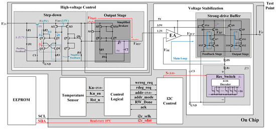
Figure 1.
Block diagram and practical circuit implementation of the proposed LDO.
2.1. Step-Down Circuit
Figure 1 illustrates the step-down circuit, which utilizes a dynamic adaptive compensation technique to reduce input voltages from 6 V to 60 V to a 5 V power supply (V5) and deliver a 3.5 V bias voltage (V3D5) for subsequent modules. Unlike conventional LDOs that use bandgap reference voltage sources, this circuit employs high-voltage-resistant devices, enabling both bias voltage provision and high-voltage control.
The diode D1 is a Zener diode. Upon reaching its reverse breakdown voltage, it undergoes reverse breakdown, causing a sharp increase in reverse current while maintaining a stable voltage across its terminals [14]. Consequently, diode D1 stabilizes the voltage at node A at 5.7 V. This stabilization ensures a consistent voltage drop across resistor R1, allowing it to function as a constant current source to limit the current. M1 is a voltage regulator employing a high-voltage depletion-type NMOS. When the input voltage is below M1’s breakdown voltage, V5 mirrors the input voltage. If the input exceeds M1’s voltage, M1 caps V5 at 5V, supplying power to subsequent circuits. Capacitor C1, connected to M1’s gate, mitigates circuit overshoot voltage. Q3, Q4, and R3 constitute a constant current source, supplying bias current to the following circuits. Q1, Q2, R2, and R3 form a proportional current mirror. Differential pair transistors Q1 and Q2 may suffer from mismatch due to process errors or environmental factors, causing a deviation of I2/I1 from the ideal 1/3 ratio.
Unlike the traditional current bias circuit, Q3, Q4, and R3 function as both a constant current source and a dynamic mismatch compensation mechanism for the current mirror, addressing mismatch issues and reducing temperature drift [15,16]. Q3 and Q4 establish a positive feedback loop. In the branch containing Q1, any change in the collector current I1 of Q1 leads to a corresponding change in the collector current I3 of Q3. This positive feedback loop causes I3 to amplify the response of the collector current I2 of Q2 to changes in I1, thereby enhancing the accuracy of the proportional current mirror. R3 is in series with the emitter of Q4, creating a negative feedback loop. In the branch containing Q2, if temperature fluctuations and process variations reduce the currents I2 and the collector current I4 of Q4, the voltage drop across R3 increases. This reduces the base-emitter voltage VBE2 of Q2, thereby mitigating the change in current amplitude. Simultaneously, R3 dampens VIN fluctuations, stabilizing I1 and I2. Together, Q3, Q4, and R3 form a coordinated mismatch compensation system using both positive and negative feedback. If the base-emitter voltage VBE1 of Q1 is slightly less than VBE2, the positive feedback reduces I2, while R3, through negative feedback, adjusts I4, aligning I1 and I2 closer to the ideal proportional mirror.
Under the condition of considering the mismatch error, the ratio of I1 to I2 can be expressed as
In the formula, β (0 < β < 1) represents the attenuation coefficient for negative feedback on error, AF denotes the positive feedback gain, and Δγ indicates the mismatch error of I2/I1. When AF × β ≈ 1, Δγ is significantly reduced, allowing I2/I1 to approach the ideal value of 1/3.
2.2. Simplified Brokaw Output Stage
In the step-down circuit, the M2 transistor functions as both a proportional current mirror load and a source of 3.5 V bias voltage (V3D5) for the subsequent circuit. Following two stages of proportional mirroring, I2 flows through the branch containing Q6 and R4, establishing a bias voltage of 1.2 V (VBIAS). However, VBIAS is notably influenced by the current ripple voltage, potentially diminishing the LDO’s PSRR.
The reference voltage VREF at the output of the simplified Brokaw output stage is
In the formula, VG0 represents the reference temperature Tr and the silicon bandgap voltage, Tr is 300 K. After simplification, we obtain
Figure 1 illustrates the proposed simplified Brokaw output stage, which streamlines the second-stage circuit of the traditional Brokaw structure [17,18]. The high-voltage control circuit and boost transistor M4 function as a clamping circuit to lower static power consumption. A low-pass filter, consisting of R7 and C2, is employed to eliminate high-frequency noise, enhancing power supply ripple rejection (PSRR) in the high-frequency range. The PSRR achieves 70.74 dB at 1 MHz.
3. Voltage Stabilization Circuit Architecture and Implementation
Figure 1 illustrates the proposed LDO voltage stabilization circuit, comprising an error amplifier, a strong-drive buffer, voltage-dividing feedback resistors (R8 and RF), a switching resistor array, and a compensation capacitor C3. The error amplifier’s architecture, detailed in Figure 2, includes three stages: a start-up circuit, a current biasing stage, and an output stage. The output stage employs a wide-swing, high-precision Cascode structure with PMOS input-pair transistors. The differential pair within the internal current reference, along with R2, establishes a negative feedback mechanism that significantly mitigates the impact of power supply voltage fluctuations on the output, thereby enhancing the PSRR and providing a robust loop frequency response and a broad input common-mode voltage range. The LDO’s output voltage VO is
Figure 2.
Structure of the error amplifier.
In the formula, RS represents the output resistance value of the resistor switch array (Res_Switch), which is controlled by the three-digit binary signal S<3:0>, and the output voltage is jointly determined by the feedback resistor network and VREF.
3.1. Strong-Drive Buffer
Figure 1 illustrates the strong-drive buffer proposed in this paper, comprising two identical stages: a feedback stage and an output stage. The output stage’s load transistor, MP, also functions as the LDO system’s power transistor. In this two-stage design, all pairs of MOS transistors, except for M6 and MP, share identical W/L ratios, ensuring VBF accurately mirrors minor output voltage variations. The power transistor MP features a large W/L ratio to handle high load currents, while M6’s smaller W/L ratio precisely mimics the feedback loop’s low current. This configuration decouples the feedback loop from the system output, shielding it from load noise interference. Consequently, the feedback loop can employ a low-current strategy that is highly sensitive to load noise, thus minimizing the system’s quiescent current. This approach enhances current efficiency while maintaining robust current-driving capability.
This buffer, utilizing the pole separation technique [19,20,21], offers dynamic compensation under varying loads, outperforming traditional source followers. In the feedback stage, an increase in load current leads to an increase in IP, a decrease in voltage at point B, and an increase in current ID14 through M14. Consequently, the current through the current mirror formed by M15 and M8 rises, resulting in a higher current ID7 through M7. This escalation causes M7’s transconductance gm7 to increase with the load current, similarly elevating the transconductance gm6 of the feedback output transistor. Based on the same structure, the output impedance RO of the buffer’s output stage is:
Formula (5) demonstrates that this strongly driven buffer effectively reduces the output resistance RO as the load current rises, thus elevating the frequency of the output pole. Figure 3 compares the loop frequency responses before and after compensation. Initially, the low-frequency pole p* splits into two high-frequency poles, p2 and p3, enhancing the loop’s gain-bandwidth product (GBW).
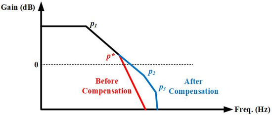
Figure 3.
Diagram of frequency compensation.
3.2. Digital Temperature Trimming
Figure 1 illustrates the digital temperature trimming technique proposed in this paper. The temperature regulation is accomplished by integrating a switch resistance array, Res_Switch, within the voltage stabilizing circuit. This system interfaces with a temperature sensor, control logic module, I2C control module, and off-chip EEPROM [22], all external to the LDO. The temperature sensor is based on a 16-bit Σ-Δ ADC architecture, and the data reading from the off-chip EEPROM is based on the I2C bus protocol [23,24,25]. The switch resistor array, Res_Switch, is governed by the four-bit binary signal S<3:0>. To balance system scale and output accuracy, the LDO’s output voltage is trimmed every 10 °C across the operating range of −40 °C to 130 °C, resulting in 18 trimming points. Prior to activation, a post-layout simulation of the LDO’s output voltage is performed. At each trimming point, S<3:0> is adjusted to minimize error, and these values are stored in separate units of the off-chip EEPROM. Upon activation, the temperature sensor outputs various control signals, Ku<15:0>, to the control logical module at different temperatures. When the control logical module receives the Ku<15:0> for a specific trimming point, it interfaces with the I2C control module. This module retrieves the corresponding S<3:0> from the off-chip EEPROM and writes it to its internal register. The S<3:0> is then sent to the switch resistor array to trim the output voltage according to temperature. It is noteworthy that the values of S<3:0> at the trimming points of 20 °C and 30 °C are identical, ensuring a unique S<3:0> value at the room temperature of 27 °C when all other conditions are identical.
Figure 4 illustrates the structure of the switch resistor array, Res_Switch. A 4-16 decoder translates S into a 16-bit thermometer code, where each bit, from the 1st to the 16th, maps to signals I0 through I15. When the control signal represents a decimal number n (0 ≤ n ≤ 15), the signal In transitions from low to high, activating the NMOS switch Mn. The series resistors R through Rn are then connected to the feedback loop, determining the total output resistance RS, as expressed in the formula
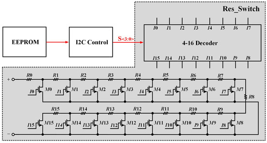
Figure 4.
Structure of the switch resistor array.
3.3. Loop Small-Signal Analysis
Figure 5 presents the small-signal equivalent circuit of the voltage regulator module loop. The output node of the first-stage amplifier features two cascaded two-stage amplifier branches. In the diagram, gm1 denotes the transconductance of the error amplifier, gm6 and gm7 represent the transconductance of M6 and M7, respectively, gmP is the transconductance of the power transistor, and gm11 is the transconductance of M11. The output resistances are Roa for the error amplifier, Ro6 for M6, Ro7 for M7, and Ro11 for M11. The output capacitances are Coa for the error amplifier, Co6 for M6, Co7 for M7, and Co11 for M11. RO and CL are the load resistance and capacitance at the output terminal. In the small-signal loop analysis, only the series branch of gm6 and gm7, which includes feedback, is considered.
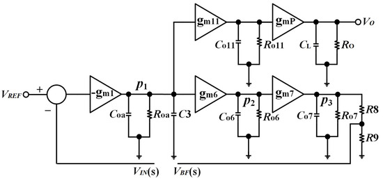
Figure 5.
The small-signal equivalent circuit diagram of the voltage stabilizing module.
Solving the nodal current equations yields the system transfer function as follows:
In Figure 3, three poles are depicted, which can be derived from the formula. With the addition of compensation capacitor C3, the first pole’s frequency shifts rightward on the coordinate axis, enhancing the phase margin and system stability. The system’s DC gain is
The gain-bandwidth product (GBW) of the system is given by the following formula:
4. Simulation Results and Discussion
The LDO circuit proposed in this paper is fabricated using the 180 nm 1P4M BCD process. The power transistor MP employs a deep P-well NMOS transistor to suppress parasitic effects. A photograph of the transmitter chip containing the proposed LDO is shown in Figure 6. The chip size is 5.88 mm2, and all on-chip digital modules are powered by the proposed LDO.
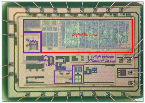
Figure 6.
Photo of transmitter chip containing LDO proposed in this paper.
Figure 7 and Figure 8 illustrate the loop stability of the voltage regulator circuit across different process corners and temperatures, with load currents from 0.1 mA to 100 mA and an input voltage of 60 V. Post-layout simulation results reveal that, irrespective of process variations and environmental conditions, the DC gain spans 80.5 dB to 100.3 dB, the minimum GBW is 875 kHz, and the phase margin is at least 61.5° (more than 60°), confirming superior loop stability. Figure 9 demonstrates that at load currents of 0.2 mA (light load), 1 mA (medium load), and 50 mA (heavy load), the PSRR ranges from 118.6 dB to 124.5 dB, underscoring the LDO’s robust power supply ripple rejection.
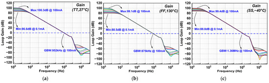
Figure 7.
Loop gains under different process corners, temperatures, and load currents. (a) TT, 27 °C; (b) FF, 130 °C; (c) SS, −40 °C.
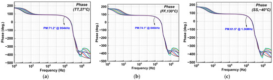
Figure 8.
Phase margins under different process corners, temperatures, and load currents. (a) TT, 27 °C; (b) FF, 130 °C; (c) SS, −40 °C.
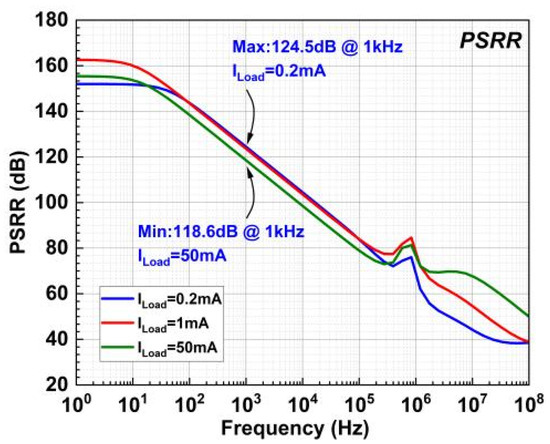
Figure 9.
PSRR under different load current levels.
Figure 10 illustrates the load and line regulation of the LDO, with a maximum line regulation of 44.2 mA and a maximum load regulation of 0.5 μV/V. Figure 11 demonstrates that across the temperature range of −40 °C to 130 °C, the maximum output voltage error decreases from 1.6% to 0.3% post-trimming, validating the effectiveness of the proposed digital trimming technique in mitigating temperature-induced voltage drift. Figure 12 depicts the LDO’s load transient response, showing an output overshoot of 32.7 mV and an undershoot of 47.2 mV when the load current changes from 0.1 mA to 100 mA at an input voltage of 6 V. At 60 V input, the loop maintains a rapid response, swiftly stabilizing the output. Figure 13 illustrates the quiescent current of the LDO across various input voltages and load currents. Across different process corners and operating temperatures, the maximum load current reaches 44.7 μA, while the minimum is 14.8 μA, highlighting its low quiescent power consumption. Figure 14 presents Monte Carlo simulation results of the LDO output voltage, aligning closely with test results under the TT process corner.
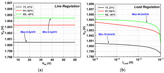
Figure 10.
(a) Line regulation of the LDO; (b) load regulation of the LDO.
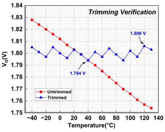
Figure 11.
Verification of the temperature trimming function of the LDO.
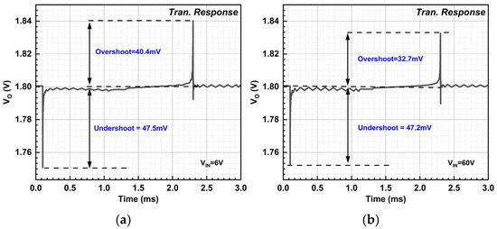
Figure 12.
Load transient response of the LDO: (a) input voltage is 6 V; (b) input voltage is 60 V.
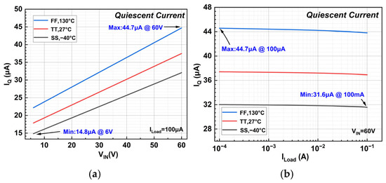
Figure 13.
The quiescent current of the LDO under different input voltages and load currents: (a) in the input voltage range of 6 V to 60 V; (b) in the load current range of 0.1 mA to 100 mA.
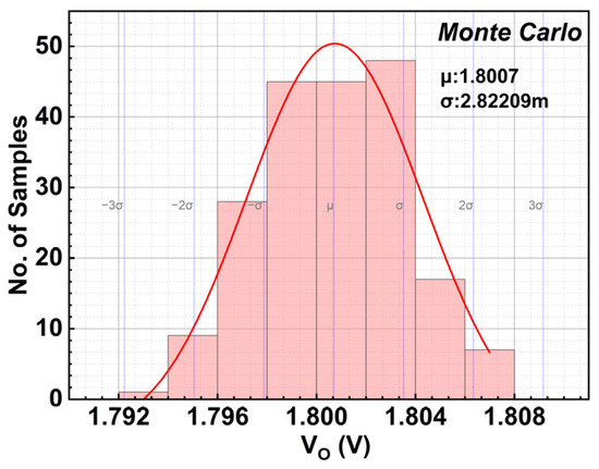
Figure 14.
Monte Carlo simulation of the output voltage of the LDO.
Table 1 presents the performance of the proposed LDO alongside comparable designs and products. The LDO demonstrates significant advantages in the input voltage range and PSRR compared to similar types. It effectively balances current driving capability and current efficiency and also includes a temperature trimming function.

Table 1.
Simulation performance of proposed LDO and comparison with other LDOs.
5. Conclusions
This paper proposes a low-dropout regulator (LDO) with digital temperature trimming, designed to meet the power supply needs of two-wire temperature transmitters. Fabricated using a 180 nm BCD process, the LDO provides a 1.8 V output. It features a two-stage design comprising the high-voltage control circuit and the voltage stabilization circuit. The high-voltage control circuit accommodates input voltages from 6 V to 60 V through dynamic mismatch compensation and a simplified Brokaw output stage. An RC low-pass filter at the output suppresses power supply ripple and enhances the power supply rejection ratio (PSRR). The voltage stabilization circuit includes a strong-drive buffer, supporting a maximum load current of 100 mA, and dynamically adjusts output impedance with the output transistor’s drain current to improve stability. A high-precision Cascode error amplifier further improves the PSRR to 124.5 dB. Digital trimming via a switched resistor array significantly reduces output voltage temperature drift. The LDO maintains a maximum output voltage error of just 0.3% across −40 °C to 130 °C, making it ideal for industrial temperature measurement circuits.
Author Contributions
Conceptualization, H.W.; methodology, H.W.; software, H.W.; validation, H.W., J.R. and M.L.; formal analysis, H.W.; investigation, J.R.; resources, J.R.; data curation, H.W.; writing—original draft preparation, H.W.; writing—review and editing, J.R. and M.L.; visualization, H.W.; supervision, J.R. and M.L.; project administration, J.R., B.L. and M.L.; funding acquisition, B.L., J.X. and W.Z. All authors have read and agreed to the published version of the manuscript.
Funding
Key Program of National Natural Science Foundation of China (No. 62531017); General Program of National Natural Science Foundation of China (No. 62371315); General Program of National Natural Science Foundation of China (No. 62571348); Liaoning Provincial Natural Science Foundation (No. 2025-MS-117).
Data Availability Statement
The data that support the findings of this study are available from the corresponding author upon reasonable request.
Conflicts of Interest
The authors declare no conflicts of interest.
References
- Prakosa, J.A.; Purwowibowo; Larassati, D. Development of Simple Method for Quality Testing of PT100 Sensors Due to Temperature Coefficient of Resistance Measurement. In Proceedings of the 2021 International Symposium on Electronics and Smart Devices (ISESD), Bandung, Indonesia, 29–30 June 2021; IEEE: New York, NY, USA, 2021; pp. 1–5. [Google Scholar]
- Arumun, J.; Eronu, E. Low-Cost 4-20 mA Loop Calibrator. J. Flow Control Meas. Amp Vis. 2023, 11, 49–63. [Google Scholar] [CrossRef]
- Park, H.; Jung, W.; Kim, M.; Lee, H.-M. A Wide-Load-Range and High-Slew Capacitor-Less NMOS LDO with Adaptive-Gain Nested Miller Compensation and Pre-Emphasis Inverse Biasing. IEEE J. Solid-State Circuits 2023, 58, 2696–2708. [Google Scholar] [CrossRef]
- Mao, X.; Lu, Y.; Martins, R.P. A scalable high-current high-accuracy dual-loop four-phase switching LDO for microprocessors. IEEE J. Solid-State Circuits 2021, 57, 1841–1853. [Google Scholar] [CrossRef]
- Li, Y.; Jiang, J.; Qu, P.; Zhao, Y.; Luo, F.; Xiao, Z. An Ultra-Low Noise and Wide Output Range LDO with BJT Input Stage and Base Current Cancellation Technique. IEEE Trans. Circuits Syst. Regul. Pap. 2025, 72, 3038–3047. [Google Scholar] [CrossRef]
- Li, W.; Chen, B.; Feng, J. An Improved Frequency Compensation Scheme for a Low Quiescent Current Low Dropout Voltage Regulator with Wide Input Voltage and Load Current Range. In Proceedings of the 2023 IEEE 15th International Conference on ASIC (ASICON), Nanjing, China, 24–27 October 2023; IEEE: New York, NY, USA, 2023; pp. 1–4. [Google Scholar] [CrossRef]
- Li, X.; Sun, J.; Qiu, M.; Wei, T.; Chen, N. Invited Paper: A 3∼45 V Input and 3.1μ A Quiescent Current LDO with Fast Transient Response for Automotive Electronics Application. In Proceedings of the 2024 IEEE International Conference on Integrated Circuits, Technologies and Applications (ICTA), Hangzhou, China, 25–27 October 2024; IEEE: New York, NY, USA, 2024; pp. 37–39. [Google Scholar] [CrossRef]
- Wei, X.; Liu, W.; Zhang, Z.; Yu, Z. A Wide Input Voltage Range LDO with Fast Transient Response. In Proceedings of the 2023 6th International Conference on Electronics Technology (ICET), Chengdu, China, 12–15 May 2023; IEEE: New York, NY, USA, 2023; pp. 114–119. [Google Scholar] [CrossRef]
- Pereira-Rial, O.; Lopez, P.; Carrillo, J.M. 0.6-V-V IN 7.0-nA-I Q 0.75-mA-I L CMOS Capacitor-Less LDO for Low-Voltage Micro-Energy-Harvested Supplies. IEEE Trans. Circuits Syst. Regul. Pap. 2022, 69, 599–608. [Google Scholar] [CrossRef]
- Xu, D.; Zhang, Y.; Luo, X.; Li, Z.; Pan, Q. A 0.96–0.9-V Fully Integrated FVF LDO with Two-Stage Cross-Coupled Error Amplifier. IEEE Trans. Circuits Syst. II Express Briefs 2023, 70, 3757–3761. [Google Scholar] [CrossRef]
- Li, Y.; Wang, L.; Wang, Y.; Wang, S.; Cui, M.; Guo, M. A Low-Power, Fast-Transient FVF-Based Output-Capacitorless LDO with Push–Pull Buffer and Adaptive Resistance Unit. Electronics 2023, 12, 1285. [Google Scholar] [CrossRef]
- He, Z.; Luo, P.; Wang, H.; Chen, J.; Song, H. A Wide-Input-Range, Low Quiescent Current LDO with E/D Reference for Piezoelectric Energy Harvesting. AEU Int. J. Electron. Commun. 2022, 157, 154419. [Google Scholar] [CrossRef]
- Li, L.; Lai, X.; Jin, D.; Shi, L.; Xu, S. An Input Up to 100-V High Voltage LDO Based a Novel Pre-Regulation and a Simple Clamp Current Circuit. Electronics 2023, 12, 3257. [Google Scholar] [CrossRef]
- Van Dorpe, P.; Liu, Z.; Van Roy, W.; Motsnyi, V.F.; Sawicki, M.; Borghs, G.; De Boeck, J. Very High Spin Polarization in GaAs by Injection from a (Ga,Mn)As Zener Diode. Appl. Phys. Lett. 2004, 84, 3495–3497. [Google Scholar] [CrossRef]
- Wang, Y.; Zhu, Z.; Yao, J.; Yang, Y. A 0.45-V, 14.6-nW CMOS Subthreshold Voltage Reference with No Resistors and No BJTs. IEEE Trans. Circuits Syst. II Express Briefs 2015, 62, 621–625. [Google Scholar] [CrossRef]
- Rincon-Mora, G.A. Analog IC Design with Low-Dropout Regulators, 2nd ed.; McGraw Hill LLC: New York, NY, USA, 2014; pp. 272–273. [Google Scholar]
- Krolak, D.; Plojhar, J.; Horsky, P. An Automotive Low-Power EMC Robust Brokaw Bandgap Voltage Reference. IEEE Trans. Electromagn. Compat. 2020, 62, 2277–2284. [Google Scholar] [CrossRef]
- Krolak, D.; Horsky, P. An EMI Susceptibility Improved, Wide Temperature Range Bandgap Voltage Reference. IEEE Trans. Electromagn. Compat. 2024, 66, 801–808. [Google Scholar] [CrossRef]
- Park, C.-J.; Onabajo, M.; Silva-Martinez, J. External Capacitor-Less Low Drop-Out Regulator with 25 dB Superior Power Supply Rejection in the 0.4–4 MHz Range. IEEE J. Solid-State Circuits 2014, 49, 486–501. [Google Scholar] [CrossRef]
- Jeon, I.; Guo, T.; Roh, J. 300 mA LDO Using 0.94 μA IQ with an Additional Feedback Path for Buffer Turn-off Under Light-Load Conditions. IEEE Access 2021, 9, 51784–51792. [Google Scholar] [CrossRef]
- Lavalle-Aviles, F.; Torres, J.; Sanchez-Sinencio, E. A High Power Supply Rejection and Fast Settling Time Capacitor-Less LDO. IEEE Trans. Power Electron. 2019, 34, 474–484. [Google Scholar] [CrossRef]
- Wang, D.-M.; Cai, J.-H.; Wu, J.; Li, D.-Z.; Hu, J.-G.; Zhong, Q.-H. A 3 Kbits of Low-Cost, Low-Power EEPROM Integrated into RFID Tag Integrated Circuits Available for Bio-Consumer Electronics. IEEE Trans. Consum. Electron. 2025, 71, 5437–5445. [Google Scholar] [CrossRef]
- Kantor, M.; Molinazzi, N.; Shmilovich, T.; Krylov, S. Low-Cost Polymeric Energy Harvester as Vibration Intensity Sensor. IEEE Sens. Lett. 2025, 9, 1–4. [Google Scholar] [CrossRef]
- Deng, C.; Sheng, Y.; Wang, S.; Hu, W.; Diao, S.; Qian, D. A CMOS Smart Temperature Sensor with Single-Point Calibration Method for Clinical Use. IEEE Trans. Circuits Syst. II Express Briefs 2016, 63, 136–140. [Google Scholar] [CrossRef]
- Albalooshi, A.; Jallad, A.-H.M.; Marpu, P.R. Fault Analysis and Mitigation Techniques of the I2C Bus for Nanosatellite Missions. IEEE Access 2023, 11, 34709–34717. [Google Scholar] [CrossRef]
- Guo, T.; Kang, W.; Roh, J. A 0.9-μA Quiescent Current High PSRR Low Dropout Regulator Using a Capacitive Feed-Forward Ripple Cancellation Technique. IEEE J. Solid-State Circuits 2022, 57, 3139–3149. [Google Scholar] [CrossRef]
- Texas Instruments. TPS7B88-Q1 500-mA, 40-V, Low-Dropout Regulator. Available online: https://www.ti.com.cn/product/cn/TPS7B88-Q1 (accessed on 26 September 2025).


Disclaimer/Publisher’s Note: The statements, opinions and data contained in all publications are solely those of the individual author(s) and contributor(s) and not of MDPI and/or the editor(s). MDPI and/or the editor(s) disclaim responsibility for any injury to people or property resulting from any ideas, methods, instructions or products referred to in the content. |
© 2025 by the authors. Licensee MDPI, Basel, Switzerland. This article is an open access article distributed under the terms and conditions of the Creative Commons Attribution (CC BY) license (https://creativecommons.org/licenses/by/4.0/).