Article

Design of High-Efficiency Concurrent Dual-Band Power Amplifier Based on Baseband and Harmonic Load Impedance Control for Wireless Communication

1
State Grid Sichuan Electric Power Research Institute, Chengdu 610041, China
2
School of Microelectronics and Communication Engineering, Chongqing University, Chongqing 400044, China
*
Author to whom correspondence should be addressed.
Electronics 2025, 14(21), 4242; https://doi.org/10.3390/electronics14214242
Submission received: 17 September 2025 / Revised: 30 September 2025 / Accepted: 29 October 2025 / Published: 30 October 2025

Abstract

The concurrent performance of a dual-band power amplifier (DBPA) is significantly influenced by baseband and harmonic load impedances. This paper presents a design methodology for high-efficiency concurrent DBPAs by controlling baseband and harmonic load impedances. An output matching network (OMN) that incorporates baseband and harmonic impedance control circuits is proposed to realize concurrent DBPAs. This OMN provides the active device with low baseband and third harmonic impedances, while simultaneously ensuring a high second harmonic load impedance. A 1.8/2.6 GHz concurrent DBPA is implemented in this paper. When evaluated using a single-tone continuous-wave (CW) signal, the fabricated PA exhibits an output power of 42.5 dBm and 41.8 dBm with drain efficiencies (DEs) of 74.2% and 77.8% at 1.8 and 2.6 GHz, respectively. Moreover, when the DBPA is measured using a balanced concurrent 1.8/2.6 GHz two-tone CW signal, the measured maximum output power is 39.9 dBm and the measured DE is 67.4%.

1. Introduction

In the 5G/6G era, the fragmentation of spectrum resources and the increasing demand for high-frequency applications have made traditional single-band power amplifiers (PAs) unable to meet the needs of multi-band parallel processing [1,2]. In contrast, concurrent dual-band PAs (DBPAs) play a pivotal role in enabling multi-band coverage and achieving high spectral efficiency [3]. Moreover, these concurrent DBPAs offer significant advantages in reducing hardware complexity and lowering deployment costs [4]. Consequently, research on concurrent DBPAs not only drives innovation in RF device design but also provides crucial technical support for enhancing spectrum sharing and improving energy efficiency [5].
While numerous studies have been conducted on high-efficiency DBPAs, the majority of them have concentrated on evaluating the performance of these DBPAs at two distinct frequency points, rather than assessing their concurrent performance capabilities [6,7,8,9]. Specifically, the concurrent performance of these DBPAs was overlooked during the design phase, despite the fact that some of these studies did incorporate concurrent two-tone signal measurements for evaluation purposes [10,11].
It has been demonstrated in many previous works that baseband load impedance has a significant effect on the concurrent performance of a DBPA [12,13,14]. In [15], the authors demonstrated that baseband load impedance is the dominant factor causing concurrent efficiency degradation. In [16], they also investigated the effect of the input baseband impedance on the efficiency of a concurrent DBPA. It can be summarized from [15,16] that even if a DBPA has excellent performance at two separate frequency points, its concurrent performance may decrease significantly due to imperfect control of the input and output baseband impedances. In [17], a baseband impedance tuning network was parallel-connected to the output matching network (OMN), enhancing the concurrent performances of a DBPA. In [18], a 2.7/3.5 GHz concurrent DBPA was implemented with baseband impedance control, achieving 40.1 dBm of saturation output power and 62.6% of saturation drain efficiency (DE) under a balanced concurrent operation mode.
In addition to baseband impedance, harmonic impedance is also crucial for improving the efficiency of a concurrent DBPA. Recently, some waveform-engineered concurrent dual-band PAs were investigated, including concurrent class-J, class-F and class-F2 PAs [18,19,20,21]. In [19], a thorough examination was conducted on the performance of the class-J PA when subjected to concurrent signal excitation. The study revealed that the concurrent class-J PA exhibits superior efficiency over its concurrent class-B counterpart. Furthermore, a concurrent dual-band class-J PA was developed, operating at 1.842 GHz and 2.35 GHz, and it attained a concurrent DE of 60%. In [20], the performance evaluation of a concurrent dual-band class-F PA was carried out, employing the same analytical approach as utilized in [19]. Meanwhile, in [22], the power series method was adopted to scrutinize the performances of a concurrent class-F2 PA. This analysis was subsequently validated through the implementation of a 1.8–2.2 GHz PA, which exhibited a concurrent output power of 40.0–40.6 dBm. Additionally, this PA achieved a concurrent DE ranging between 60.0% and 64.0% across a tone spacing of 0–400 MHz.
In this paper, we introduce an innovative design methodology aimed at implementing high-efficiency concurrent DBPAs. Recognizing the pivotal role of baseband and harmonic load impedances in enhancing concurrent efficiency [22,23], we developed an OMN that incorporates baseband and harmonic impedance control circuits. This OMN provides the active device with low baseband and third harmonic impedances, while simultaneously ensuring a high second harmonic load impedance. In this way, the concurrent DBPA operates in an inverse class-F mode at its two operational frequency points, thereby boosting its overall efficiency. We have successfully designed and fabricated a high-efficiency concurrent DBPA operating at 1.8/2.6 GHz. This PA delivers a concurrent output power of 39.9 dBm and attains a DE of 67.4% at its saturation power level.

2. Design Considerations of High-Efficiency Concurrent DBPA

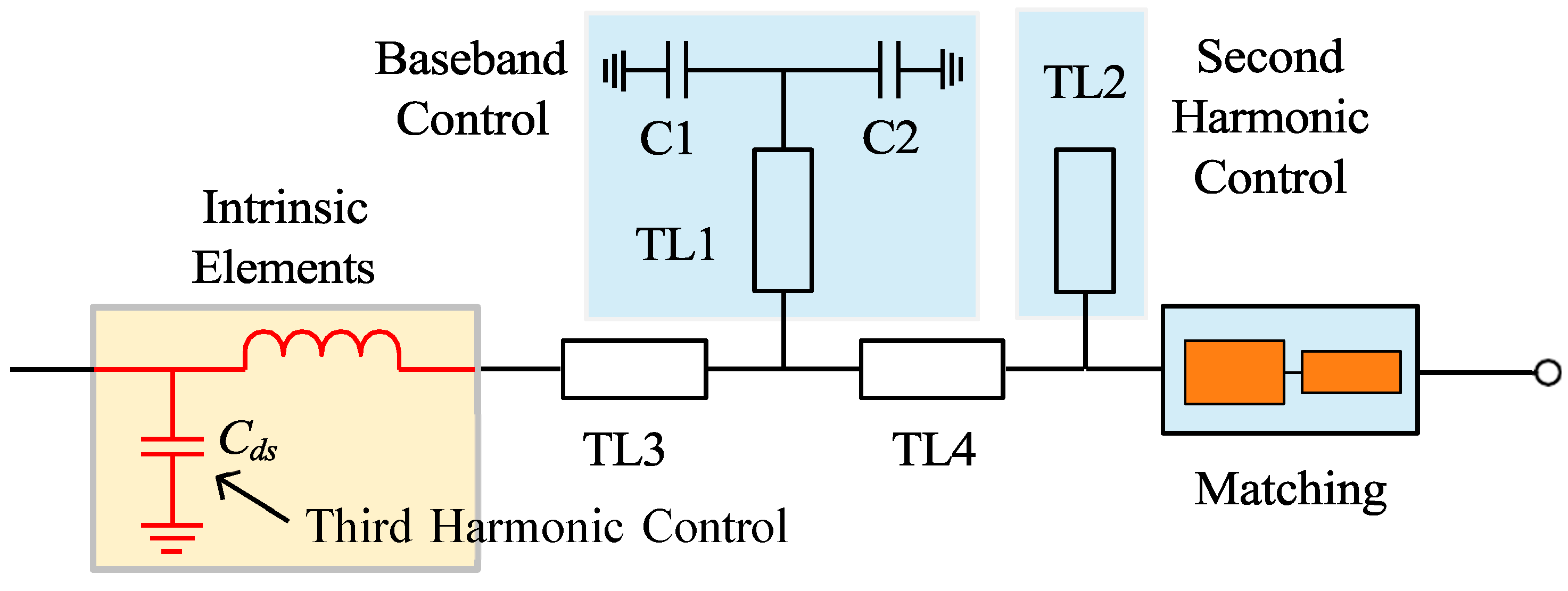
In this study, our focus is on designing a high-efficiency concurrent DBPA, with careful consideration given to both baseband and harmonic load impedances. Figure 1 presents the block diagram of the proposed concurrent DBPA. The active transistor is modeled as an ideal voltage-controlled current source, along with its intrinsic elements. Beyond the active device, the concurrent DBPA incorporates a dual-band input matching network (IMN) and an OMN to ensure optimal performance. Notice that a baseband control and harmonic control circuits are integrated into the OMN.
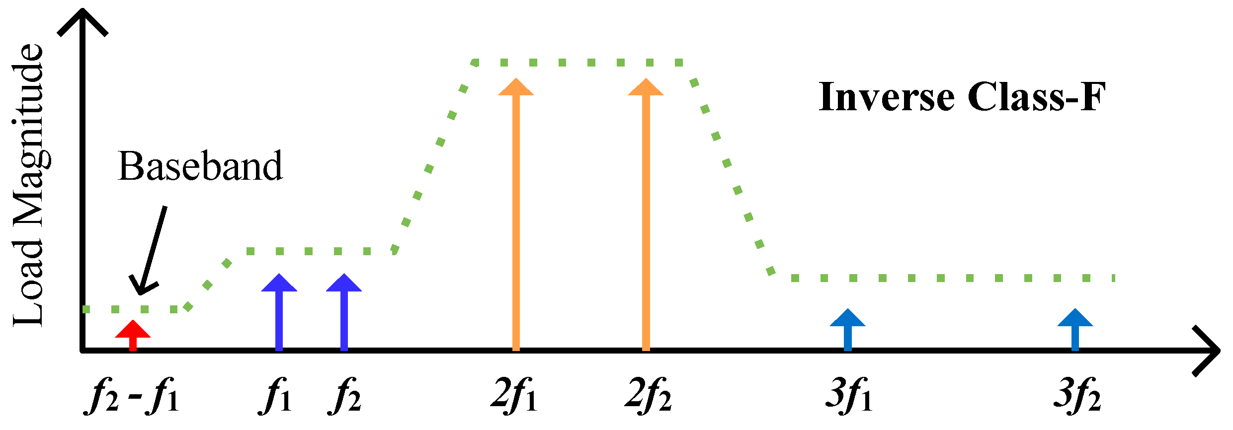
In our design, an OMN architecture shown in Figure 2 is utilized. A low baseband impedance is realized using the transmission line TL1 and the capacitors C1 and C2. This baseband impedance control circuit (BICC) presents low impedance at a low frequency band and high impedance at the fundamental frequency. Take note that the intrinsic elements and the transmission line TL3 have a negligible phase delay at the baseband frequency.
Therefore, the baseband impedance at the device intrinsic plane is mainly provided by the BICC. And this BICC has very little effect on the matching condition at the fundamental and harmonic frequencies.
To achieve an even greater improvement in concurrent efficiency, we have implemented precise control over the second and third harmonic load impedances, tailoring them to meet the specific harmonic requirements of the inverse class-F PA [24]. In other words, it is essential to attain high impedance for the second harmonic and low impedance for the third harmonic at the transistor intrinsic plane. The control of the second harmonic impedance is primarily achieved through the use of transmission line TL2, which creates a short circuit at the second harmonic frequency along the main path. Subsequently, the initially low second harmonic impedance is transformed into high impedance via the combined action of TL4, TL3, and the intrinsic elements of the transistor. Regarding the third harmonic load impedance, it is mainly controlled by the drain capacitor Cds of the transistors, as demonstrated in [25]. Following the meticulous control of the baseband, second, and third harmonic load impedances, an additional matching network was implemented to ensure proper fundamental impedance matching.
When designing the OMN, the optimization function in the Advanced Design System (ADS) software (version 2023) is utilized. The OMN is firstly constructed based on the architecture shown in Figure 2. Then, an initial value is assigned to the width and length of each transmission line. Finally, the widths and lengths of the transmission lines are optimized to meet the impedance requirements shown in Figure 3.

3. Design and Simulation of a Concurrent Dual-Band PA

Utilizing the aforementioned design methodology, this section details the design of a high-efficiency concurrent DBPA, which operates at 1.8/2.6 GHz. The active device is the CG2H40010F transistor from Wolfspeed. The concurrent DBPA is fabricated on a 4350B substrate form Rogers corporation, which features a thickness of 20 mil and a dielectric constant of 3.66. In this design, the transistor employed is biased with a gate voltage of −3.0 V and a drain voltage of 28 V.
Based on the theory of the inverse class-F PA, the fundamental impedance at the transistor intrinsic plane is set to 36 Ω [26]. Using this fundamental impedance, the OMN is designed and optimized using the ADS software.
The load impedances for the baseband and third harmonic frequencies are optimized to be as low as feasible, whereas the second harmonic load impedance is optimized to be as high as possible. Leveraging the structure illustrated in Figure 2, the schematic of the OMN designed for the concurrent DBPA is presented in Figure 4. This figure also includes the dimensions of all passive components. Additionally, an IMN is constructed and optimized using the ADS software. The primary purpose of this IMN is to ensure that the PA achieves high gain at the two desired frequency points. The schematic of the designed IMN, along with the dimensions of its passive elements, is also depicted in Figure 4.
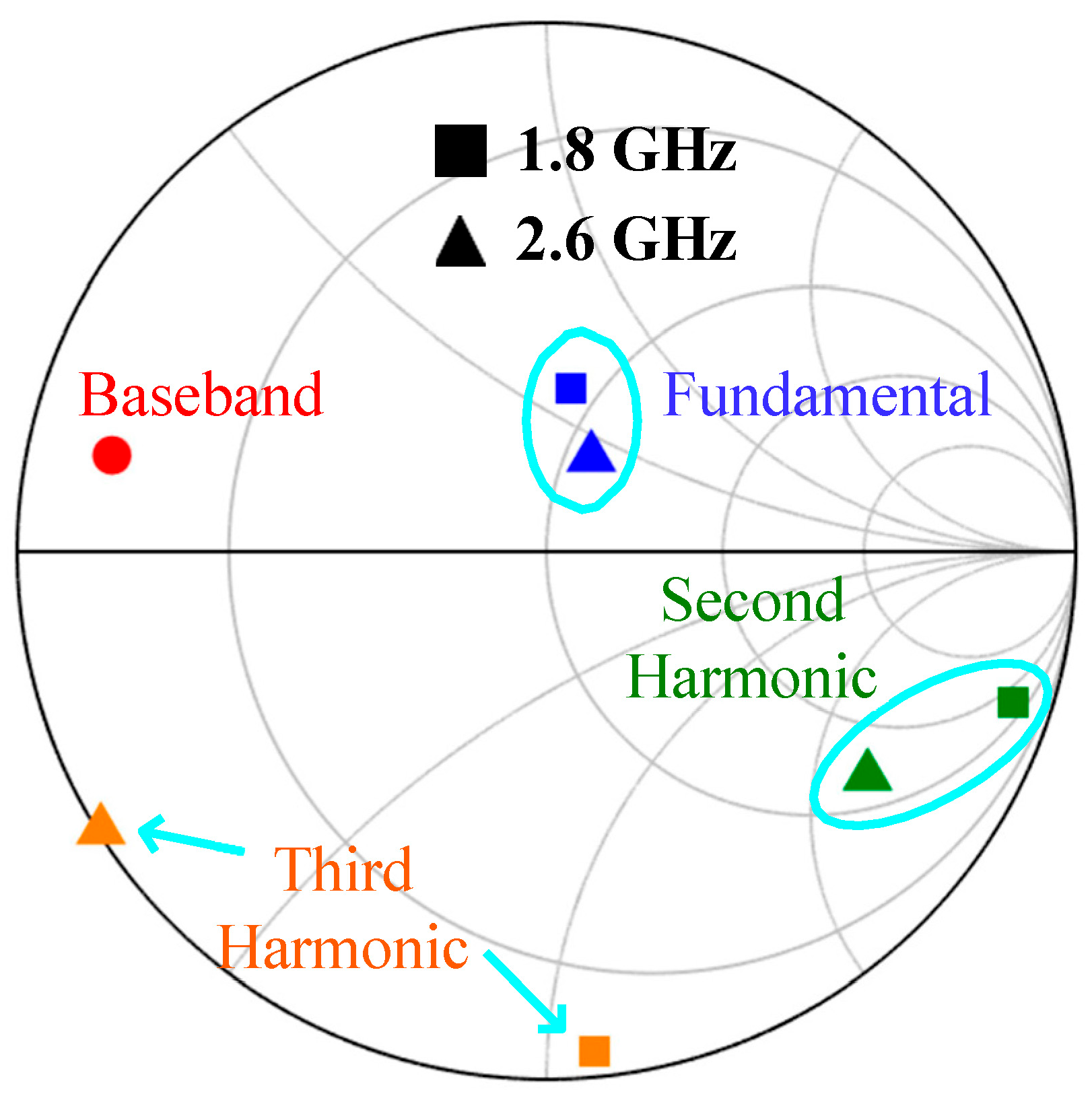
By employing the schematic of the concurrent DBPA depicted in Figure 4, the load impedance of the OMN is firstly simulated. Figure 5 displays the simulated load impedance of the designed concurrent DBPA at the intrinsic plane of the transistor (taking into account the intrinsic elements of the transistor during the simulation). The reference impedance of the Smith chart is 36 Ω. From Figure 5, it is evident that the concurrent DBPA exhibits a low impedance at both the baseband and third harmonic frequencies. Furthermore, the fundamental load impedance of the concurrent DBPA demonstrates positive reactive components at its two operational frequencies. Consequently, the second harmonic load impedance should exhibit negative reactive components at these same operational frequencies [26].
This observation is confirmed by the simulated second harmonic load impedance presented in Figure 5. Notice that the concurrent DBPA sees a slightly higher third harmonic load impedance at 1.8 GHz. This may affect the DE of the PA at 1.8 GHz.
Secondly, the designed concurrent DBPA undergoes simulation with a single-tone CW signal. At the saturation power level, the simulated waveforms of the drain voltage and current are illustrated in Figure 6. Examining Figure 6a, it is evident that the designed concurrent DBPA generates half-sinusoidal voltage and squared current waveforms at 1.8 GHz, meeting the criteria for an inverse class-F PA. Similarly, comparable voltage and current waveforms are also produced by the designed DBPA at 2.6 GHz, as depicted in Figure 6b.
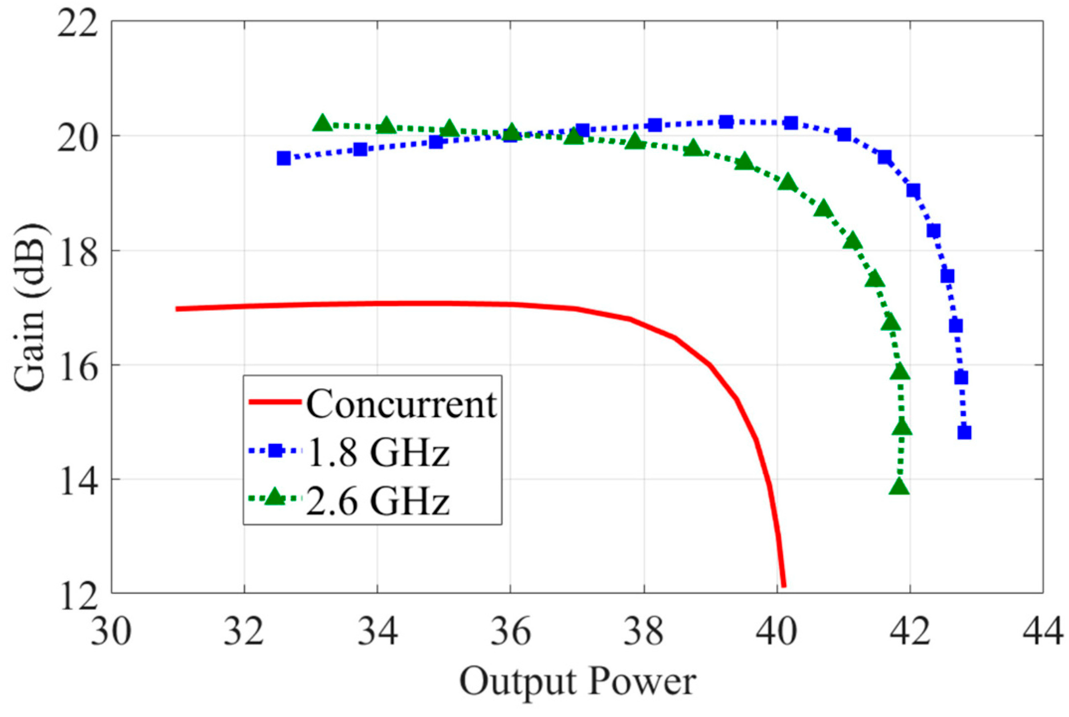
Upon exciting the designed PA with a single-tone CW signal, the simulated DEs as a function of output power at both 1.8 GHz and 2.6 GHz are presented in Figure 7. This figure reveals that the concurrent dual-band PA attains a peak output power of 42.8 dBm and a saturation DE of 76.0% at 1.8 GHz. Similarly, at 2.6 GHz, the simulated maximum output power and saturation DE for the concurrent dual-band PA are 41.9 dBm and 78.8%, respectively, as depicted in Figure 7. Furthermore, the simulated gains versus output power for the concurrent DBPA at these two frequencies are illustrated in Figure 8. The simulated saturation gains of the designed PA are 14.8 dB at 1.8 GHz and 13.9 dB at 2.6 GHz.
Thirdly, a concurrent CW signal operating at 1.8/2.6 GHz is employed to simulate the performance of the designed concurrent DBPA. The simulated concurrent DE as a function of concurrent output power is depicted in Figure 7. This figure demonstrates that the designed PA achieves a concurrent output power of 40.1 dBm, accompanied by a concurrent DE of 73.5%. Theoretically, the concurrent DE of a class-B PA is π/4 times that of its single-tone DE. Hence, the designed concurrent dual-band PA exhibits an improved concurrent DE through the control of baseband and harmonic load impedances. The simulated concurrent gain of the designed PA is presented in Figure 8. At the saturation power level, the simulated concurrent gain of the designed PA reaches 12.1 dB. Furthermore, the simulated output power at 1.8 GHz and 2.6 GHz under the balanced concurrent mode is shown in Figure 9.
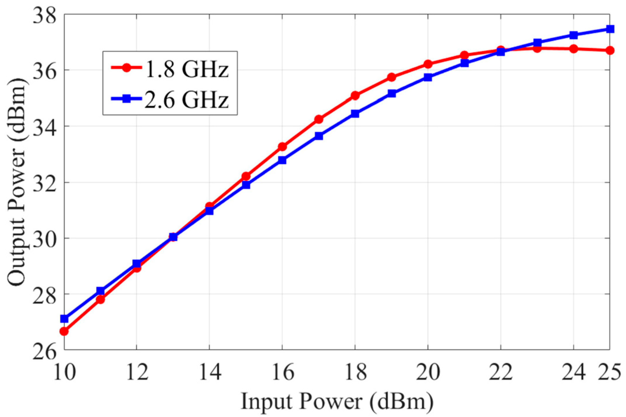
According to Figure 9, the concurrent PA delivers a maximum power of 36.7 dBm at 1.8 GHz and 37.5 dBm at 2.6 GHz. Notably, under the balanced concurrent mode, the output power of the designed concurrent DBPA remains nearly identical at both 1.8 GHz and 2.6 GHz.

4. Experimental Results

Figure 10 shows the photograph of the fabricated concurrent dual-band PA. The fabricated PA is biased with a gate voltage of −2.85 V and a drain voltage of 28 V.
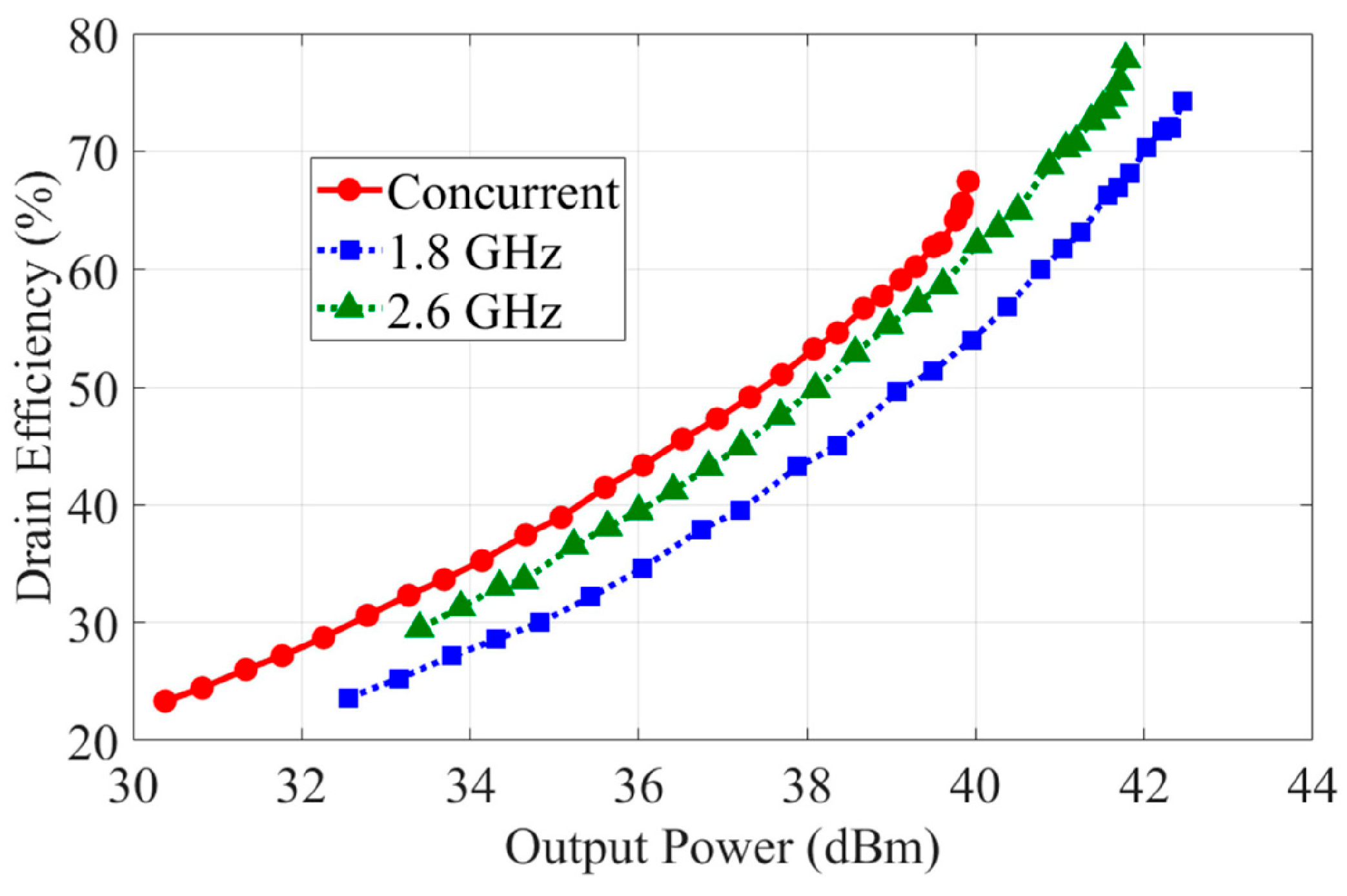
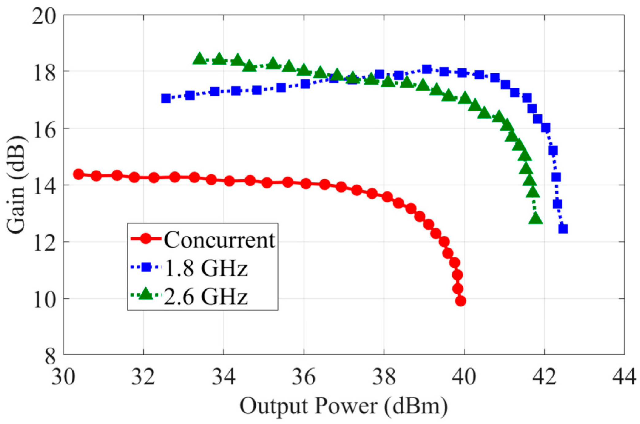
The fabricated concurrent DBPA is first tested using a single-tone CW signal. Figure 11 presents the measured DEs of the fabricated PA as a function of output power at both 1.8 GHz and 2.6 GHz. The results indicate that the fabricated concurrent DBPA achieves a maximum output power of 42.5 dBm at 1.8 GHz and 41.8 dBm at 2.6 GHz. Additionally, the measured saturation DEs of the fabricated PA are 74.2% at 1.8 GHz and 77.8% at 2.6 GHz. Figure 12 displays the measured gains versus output power for the fabricated concurrent DBPA at these two frequencies. This PA attains saturation gains of 12.5 dB at 1.8 GHz and 12.8 dB at 2.6 GHz.
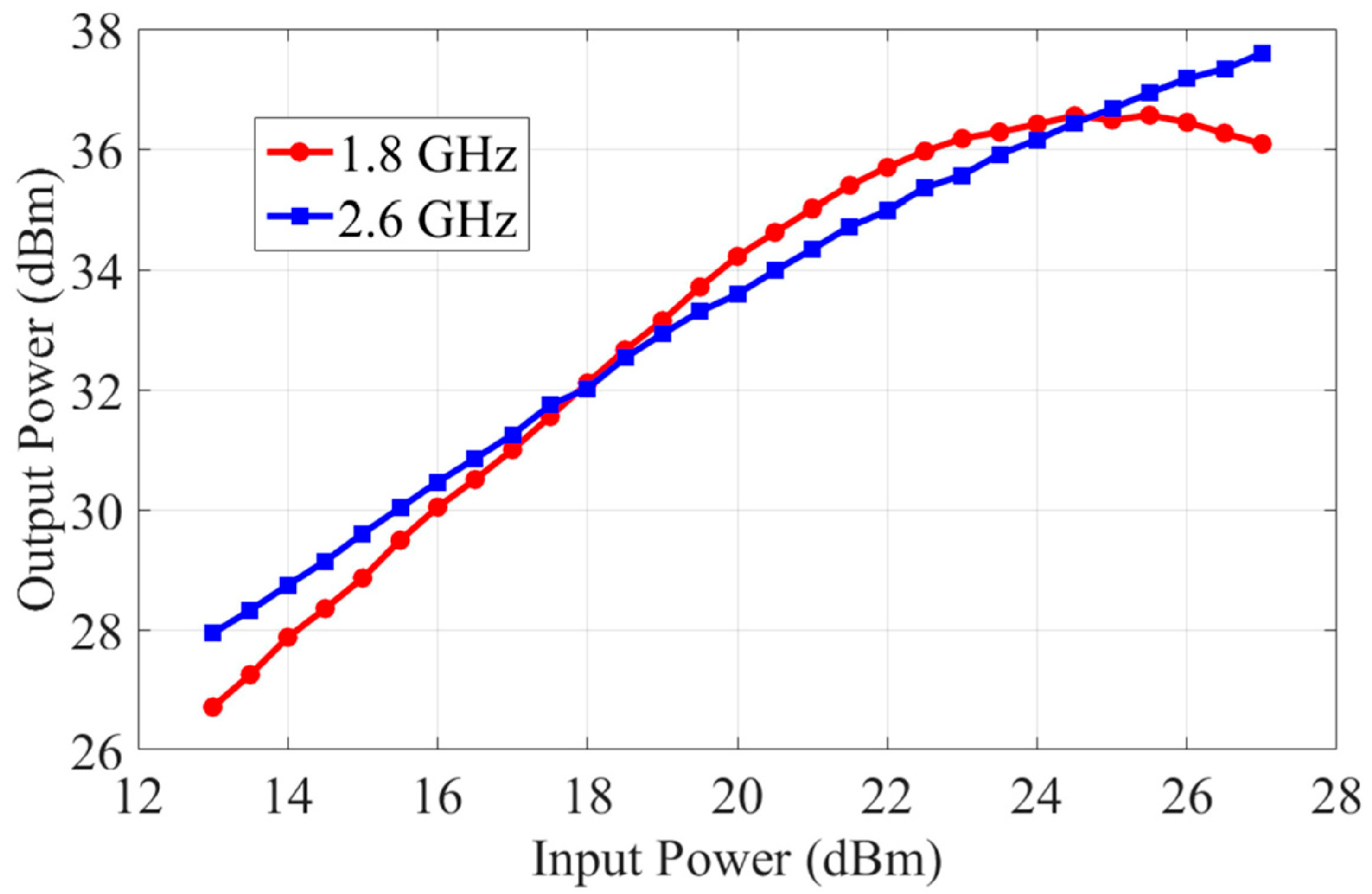
Secondly, the fabricated concurrent DBPA is tested using a balanced concurrent CW signal at 1.8/2.6 GHz. The measured concurrent DE as a function of output power is depicted in Figure 11. The results reveal that the fabricated PA attains a maximum concurrent output power of 39.9 dBm and a saturation concurrent DE of 67.4%. The measured concurrent gain of the designed PA is presented in Figure 12, indicating that the saturation concurrent gain of the fabricated DBPA is 9.9 dB. Under the balanced concurrent mode, the measured output power of the fabricated PA at 1.8 GHz and 2.6 GHz is illustrated in Figure 13. This figure demonstrates that the fabricated PA achieves a maximum power of 36.1 dBm at 1.8 GHz and 37.6 dBm at 2.6 GHz, respectively.
Compared with the simulation results, the measurement results have deteriorated to a certain extent. This may be caused by the actual passive elements having larger losses. Secondly, the utilized actual active and passive components may differ from their simulation models.
The measurement results of the fabricated concurrent DBPA are summarized in Table 1. Additionally, this table incorporates data from several concurrent DBPAs for comparative analysis. As evident from Table 1, the fabricated concurrent DBPA demonstrates a notably improved concurrent efficiency compared to other state-of-the-art works.

5. Conclusions

This paper introduces the design of a highly efficient concurrent DBPA that leverages baseband and harmonic load impedance control techniques. The baseband and harmonic control circuits are integrated within the OMN. This OMN is engineered to supply the active device with low impedances at the baseband and third harmonic frequencies, while simultaneously presenting a high impedance at the second harmonic frequency. Consequently, the dual-band PA operates in an inverse class-F mode across its two designated operating frequencies. A prototype of a high-efficiency concurrent DBPA, operating at 1.8 GHz and 2.6 GHz, has been successfully implemented. When excited by a balanced concurrent CW signal, the fabricated PA achieves a maximum output power of 39.9 dBm, coupled with a DE of 67.4%.

Author Contributions

Writing—original draft preparation, X.M., F.L. and S.F.; writing—review and editing, X.L. (Xi Liu), X.L. (Xiaojiang Liu) and W.S.; supervision, W.S. All authors have read and agreed to the published version of the manuscript.

Funding

This research was funded by the Science and Technology Project of State Grid Sichuan Electric Power Company “Multi-dimensional Collaborative Anomaly—Awakening Sensor Network Technology for Transmission Lines in Complex Environments” (52199723000S).

Data Availability Statement

Data are contained within the article.

Conflicts of Interest

Authors Xiaomin Ma, Fan Liu, Songhai Fan, Xi Liu and Xiaojiang Liu were employed by the company State Grid Sichuan Electric Power Research Institute. The remaining authors declare that the research was conducted in the absence of any commercial or financial relationships that could be construed as a potential conflict of interest. The authors declare that this study received funding from Science and Technology Project of State Grid Sichuan Electric Power Company. The funder was not involved in the study design, collection, analysis, interpretation of data, the writing of this article or the decision to submit it for publication.

References

  1. Wei, Z.; Liu, H.; Yang, X.; Jiang, W.; Wu, H.; Li, X.; Feng, Z. Carrier aggregation enabled integrated sensing and communication signal design and processing. IEEE Trans. Veh. Technol. 2024, 73, 3580–3596. [Google Scholar] [CrossRef]
  2. Wang, H.; Chen, Y.; Kong, W.; Qi, J.; Zheng, Z.; Xia, J. Design of wideband power amplifier using improved particle swarm optimization with output power and efficiency constraints. Electronics 2025, 14, 2813. [Google Scholar] [CrossRef]
  3. Barradas, F.M.; Nunes, L.C.; Louro, J.; Barros, D.R.; Cabral, P.M.; Pedro, J.C. The effect of IMD drain impedances in RF PA concurrent dual-band operation. IEEE Trans. Microw. Theory Tech. 2023, 71, 2920–2933. [Google Scholar] [CrossRef]
  4. Liu, K.; Shi, W.; Lu, N.; Li, Y.; Liu, J.; Zang, Y.; Hu, C.; Li, M. Broadband Doherty power amplifier with baseband impedance control for concurrent application. AEU-Int. J. Electron. Commun. 2025, 191, 155680. [Google Scholar] [CrossRef]
  5. Tao, M.; Chen, Y.; Kong, W.; Ni, S.; Zheng, Z.; Xia, J. Design of dual-mode multi-band Doherty power amplifier employing impedance-and-phase constrained optimization. Electronics 2025, 14, 2078. [Google Scholar] [CrossRef]
  6. Liu, W.; Liu, Q.; Du, G.; Li, G. Analytical dual-band matching approach for concurrent high-efficiency power amplifiers. IEEE Trans. Circuits Syst. II Express Briefs 2022, 69, 4769–4773. [Google Scholar] [CrossRef]
  7. Der, A.T.; Barton, T.W. C/Ka concurrent dual-band GaN MMIC based on shorted quarter-wavelength line topology. IEEE J. Microw. 2024, 4, 372–380. [Google Scholar] [CrossRef]
  8. Han, K.; Geng, L. Design of 0.6–0.8-GHz and 1.6–1.9-GHz dual-band PA with peak PAEs of over 70% by NPE method with dynamical continuous-mode criteria. IEEE Microw. Wirel. Compon. Lett. 2021, 31, 873–876. [Google Scholar] [CrossRef]
  9. Wei, L.; Chen, F.; Zhang, Z. Design of dual-band power amplifier based on microstrip coupled-line bandstop filter. AEU-Int. J. Electron. Commun. 2024, 183, 155381. [Google Scholar] [CrossRef]
  10. Cai, Q.; Che, W.; Ma, K.; Gu, L. A concurrent dual-band high-efficiency power amplifier with a novel harmonic control network. IEEE Microw. Wirel. Compon. Lett. 2018, 28, 918–920. [Google Scholar] [CrossRef]
  11. Yang, Z.; Yao, Y.; Li, M.; Jin, Y.; Li, T.; Geng, Z.; Yu, Z. A precise harmonic control technique for high efficiency concurrent dual-band continuous class-F power amplifier. IEEE Access 2018, 6, 51864–51874. [Google Scholar] [CrossRef]
  12. Ahn, K.H.; Jeong, Y.H.; Lee, S.H. Effects of source and load impedance on the intermodulation products of GaAs FETs. IEEE MTT-S Int. Microw. Symp. Dig. 2000, 1, 469–472. [Google Scholar]
  13. Brinkhoff, J.; Parker, A.E. Effect of baseband impedance on FET intermodulation. IEEE Trans. Microw. Theory Techn. 2003, 51, 1045–1051. [Google Scholar] [CrossRef]
  14. Chen, X.; Chen, W.; Ghannouchi, F.M.; Feng, Z.; Liu, Y. Enhanced analysis and design method of concurrent dual-band power amplifiers with intermodulation impedance tuning. IEEE Trans. Microw. Theory Techn. 2013, 61, 4544–4558. [Google Scholar] [CrossRef]
  15. Nunes, L.C.; Barros, D.R.; Cabral, P.M.; Pedro, J.C. Efficiency degradation analysis in wideband power amplifiers. IEEE Trans. Microw. Theory Techn. 2018, 66, 5640–5651. [Google Scholar] [CrossRef]
  16. Barros, D.R.; Nunes, L.C.; Cabral, P.M.; Pedro, J.C. Impact of the input baseband terminations on the efficiency of wideband power amplifiers under concurrent band operation. IEEE Trans. Microw. Theory Techn. 2019, 67, 5127–5138. [Google Scholar] [CrossRef]
  17. Li, J.; Chen, W.; Huang, F.; Feng, Z. Multiband and multimode concurrent PA with novel intermodulation tuning network for linearity improvement. IEEE Microw. Wirel. Compon. Lett. 2018, 28, 248–250. [Google Scholar] [CrossRef]
  18. Qi, T.; He, S.; Hu, B.; Liu, C.; Du, X.; Zhao, Y.; Helaoui, M.; Chen, W.; Ghannouchi, F.M. Efficiency analysis of concurrently driven power amplifiers. IEEE Access 2020, 8, 91379–91393. [Google Scholar] [CrossRef]
  19. Shariatifar, M.; Jalali, M.; Abdipour, A. Design of a high-efficiency dual-band class-J/J power amplifier considering concurrent mode input drive. Int. J. RF Microw. Comput. Aided Eng. 2019, 30, e22064. [Google Scholar] [CrossRef]
  20. Shariatifar, M.; Jalali, M.; Abdipour, A. A concurrent dual-band continuous Class-F power amplifier with intermodulation impedance tuning: Analysis and design technique. AEU-Int. J. Electron. Commun. 2019, 111, 152899. [Google Scholar] [CrossRef]
  21. Huang, H.; Yu, C.; Wu, Y.; Jin, Q.; Fan, C.; Gao, J.; Liu, Y. Analysis and design of a novel concurrent class B/J continuum power amplifier. Int. J. RF Microw. Comput. Aided Eng. 2020, 30, e22275. [Google Scholar] [CrossRef]
  22. Liu, J.; Shi, W.; Zang, Y.; Hua, J.; Xu, G.; Hu, C.; Liu, K.; Li, Y.; Li, M. Analysis and design of concurrent class-F2 power amplifier based on power-series technique. AEU-Int. J. Electron. Commun. 2025, 193, 155722. [Google Scholar] [CrossRef]
  23. Bunz, B.; Ahmed, A.; Kompa, G. Influence of envelope impedance termination on RF behaviour of GaN HEMT power devices. In Proceedings of the European Gallium Arsenide and Other Semiconductor Application Symposium, GAAS 2005, Paris, France, 3–4 October 2005; pp. 649–652. [Google Scholar]
  24. Dong, Y.; Mao, L.; Xie, S. Extended continuous inverse class-F power amplifiers with class-AB bias conditions. IEEE Microw. Wirel. Compon. Lett. 2017, 27, 368–370. [Google Scholar] [CrossRef]
  25. Sun, Y.; Zhu, X.W.; Zhai, J.; Zhang, L.; Meng, F. Highly efficient concurrent power amplifier with controllable modes. IEEE Trans. Microw. Theory Tech. 2015, 63, 4051–4060. [Google Scholar] [CrossRef]
  26. Song, K.; He, A.; Li, Q. Hybrid continuous inverse class-F high-efficiency power amplifier based on phase shift analysis. Microw. Opt. Technol. Lett. 2023, 65, 567–572. [Google Scholar] [CrossRef]
Figure 1. Block diagram of the proposed concurrent DBPA.
Electronics 14 04242 g001
Figure 2. Structure of the OMN for the concurrent DBPA.
Electronics 14 04242 g002
Figure 3. Load impedance trajectory of concurrent DBPA over baseband, fundamental and harmonic frequencies.
Electronics 14 04242 g003
Figure 4. Schematic of the designed concurrent DBPA.
Electronics 14 04242 g004
Figure 5. Simulated load impedance trajectory of the designed concurrent dual-band PA at the intrinsic plane.
Electronics 14 04242 g005
Figure 6. Simulated waveforms of the drain voltage and current at (a) 1.8 GHz and (b) 2.6 GHz.
Electronics 14 04242 g006
Figure 7. Simulated drain efficiencies of the designed concurrent DBPA versus output power.
Electronics 14 04242 g007
Figure 8. Simulated gains of the designed concurrent DBPA versus output power.
Electronics 14 04242 g008
Figure 9. Simulated output power of the designed concurrent DBPA at 1.8 and 2.6 GHz when it is driven by a balanced concurrent CW signal.
Electronics 14 04242 g009
Figure 10. Photograph of the fabricated concurrent DBPA.
Electronics 14 04242 g010
Figure 11. Measured DEs of the designed concurrent DBPA versus output power.
Electronics 14 04242 g011
Figure 12. Measured gains of the designed concurrent DBPA versus output power.
Electronics 14 04242 g012
Figure 13. Measured output power of the designed concurrent DBPA at 1.8 and 2.6 GHz when it is driven by a balanced concurrent CW signal.
Electronics 14 04242 g013
Table 1. Measurement results of the state-of-the art concurrent DBPAs.
Ref. (Year)Single-ToneConcurrent Two-Tone
Frequency (GHz)Power (dBm)ηD (%)Gain (dB)Tone Spacing (MHz)Power (dBm)ηD (%)Gain (dB)
[3] 20231.8/2.243.6/44.4 *67/70 *12/12.2 *40041.857 *N/A
[14] 20131.9/2.641.5/41.5 *75/70 *10.2/11 *70039.7 *63 *N/A
[15] 20181.8–2.249.5–50.5 *70–74 *N/A0–400N/A60–67 *N/A
[18] 20202.5/3.741.8/41.277.5/71.910.3/11.2 *120040.162.610.7 *
[20] 20191.842/2.65541/40.573.5/71.711/10.581339.5 *60N/A
[21] 20201.9/2.3543.7/43.173.9/60.312.3/10.645042.160.4N/A
[22] 20251.8–2.241.1–42.461.8–67.314.8–16.30–40040.0–40.660.0–64.014.9–17.8
This Work1.8/2.641.1–42.461.8–67.314.8–16.380039.967.4%9.9
* Read from graphs.
Disclaimer/Publisher’s Note: The statements, opinions and data contained in all publications are solely those of the individual author(s) and contributor(s) and not of MDPI and/or the editor(s). MDPI and/or the editor(s) disclaim responsibility for any injury to people or property resulting from any ideas, methods, instructions or products referred to in the content.