Abstract
To mitigate potential interference in a coexisting system, an ultra-wideband (UWB) antenna with triple-band-notched characteristics is proposed. Based on transmission line theory, three notched bands are achieved by utilizing the open- or short-circuited properties of microstrip line resonators and slot resonators. Each antenna element consists of a patch etched with three half-wavelength slots and a one-wavelength strip. Measurement results demonstrate that the antenna exhibits excellent rejection performance at the three designated frequency bands. Furthermore, the effects of array configuration and element deflection angle on mutual coupling are investigated using a 2 × 1 face-to-face multiple-in, multiple-out (MIMO) array. Finally, a two-element MIMO array with high isolation was fabricated and measured. Experimental results show that an isolation level better than 24.6 dB is maintained across the operating band.
1. Introduction
With the increasing performance demands of current and future wireless communication systems, antenna design is facing increasingly stringent challenges. UWB communication has emerged as a prominent research focus due to its capability for high-speed data transmission and inherently low spectral power density [1]. This growing interest has led to extensive investigations into a wide variety of UWB antenna configurations by researchers worldwide [2,3,4]. However, the broad frequency range covered by UWB systems overlaps several narrowband wireless communication standards, which have already been allocated and are in active use. These narrow bands include EMTC (1.43–1.444 GHz), N41 (2.515–2.675 GHz), and WiMAX service (3.3–3.6 GHz). This spectral coexistence inevitably introduces interference, degrading the communication performance of UWB systems. To mitigate such coexistence-induced interference without relying on external band-stop filters, it is essential to integrate band-notched functionalities directly into the UWB antenna structure [5]. This approach not only enhances the system’s interference immunity but also contributes to antenna miniaturization and improved system-level integration. An alternative approach involves integrating parasitic components to design a multi-band antenna, eliminating the need to specifically suppress certain undesired frequency bands [6,7]. However, this method is often challenging to implement in ultra-wideband (UWB) designs due to the complexity of managing broad frequency ranges.
To date, various UWB antennas with single-band-notched characteristics have been proposed [8,9,10,11,12,13]. Common techniques for realizing a single notched band include etching half-wavelength slots [8], incorporating spur-line structures [9], coupling rectangular metal strips [10], loading H-shaped metallic elements [11], introducing parasitic patches [12], and employing open-ended quarter-wavelength slots [13]. For instance, in [11], the authors presented an enhanced H-shaped conductor-backed plane, which exhibited significant band-notched performance in the 5.1–5.9 GHz range. This design also featured tunable notch center frequency and bandwidth.
To meet the increasing demand for suppressing multi-band interference in complex electromagnetic environments, UWB antennas with multi-band notch characteristics have been extensively studied and reported [14,15,16,17,18,19,20,21,22,23]. In the design of dual-band notched antennas, researchers have proposed a variety of structural solutions, such as loading dual C-shaped slots [14], combining T-shaped and U-shaped stubs [15], employing fork-shaped structure [16], introducing rectangular one-third wavelength metal strips and quarter-wavelength open-ended slots [17], utilizing quasi-complementary split-ring resonators (quasi-CSRRs) [18], and adopting two short-circuited folded stepped impedance resonators [19]. In [16], a fork-shaped parasitic structure was implemented, and, by exciting its dominant and second-order modes, effective dual-notch behavior was achieved at 3.8 GHz and 5.5 GHz. To further achieve triple-band notching, researchers have explored more complex geometries, such as combinations of elliptical CSRRs and rectangular SRRs [20], dual square slot structures [21], modified multi-mode electronic ring resonators (ERRs) [22], and enhanced H-shaped resonators [23]. In [22], a cascaded ERR design was proposed, utilizing three resonant modes to realize notched bands at 3.5 GHz, 5.8 GHz, and 7.5 GHz.
Furthermore, MIMO technology has been widely adopted in UWB communication systems due to its significant advantages in mitigating multipath fading, enhancing system capacity, and improving reliability [24]. Numerous studies have reported UWB MIMO systems based on multi-antenna configurations [25,26,27,28,29,30,31,32,33,34,35,36,37]. For instance, in [25], two antennas were arranged orthogonally with a narrow slot introduced in the ground plane to effectively suppress mutual coupling, achieving isolation greater than 15 dB across the entire 3.1–10.6 GHz band. In [26], a combination of T-shaped grounded stubs and vertical slots were utilized to obtain antenna isolation exceeding 15 dB. Meanwhile, in [30], a stepped dielectric resonator combined with an improved neutralization line structure and a square quarter-wavelength patch was designed to optimize isolation performance at both low and high frequencies, resulting in an overall isolation above 17 dB across the operating band. Although these methods have demonstrated excellent isolation for side-by-side antenna configurations, comparatively fewer studies have focused on MIMO antenna systems with symmetrical face-to-face layouts. Therefore, in-depth research on multi-band notch UWB antenna designs and their application in face-to-face dual-antenna MIMO systems is both theoretically significant and important for practical engineering.
In view of this, this paper proposes and reports a UWB antenna with tri-band-notched characteristics, along with its corresponding MIMO array design, simulation analysis, and experimental validation. By integrating a C-shaped slot, two U-shaped slots, and a C-shaped strip within the UWB patch antenna, tri-band-notched features are successfully realized over a wide impedance bandwidth, effectively filtering out specific frequency bands that may cause system interference. Furthermore, to address the requirements of MIMO communications, this study investigates a 2 × 1 MIMO array composed of two face-to-face-arranged antenna elements. The array performance under various rotational angles is analyzed to optimize inter-element isolation.
2. Tri-Band-Notched UWB Antenna Design
2.1. Band-Notched Mechanism
For a transmission line model, as shown in Figure 1a, the reflection coefficient at the load can be expressed as
where and represent the load and the characteristic impedance of transmission line, respectively. When the load impedance is either zero (short-circuited) or infinite (open-circuited), the reflection coefficient , as defined in Equation (1), becomes −1 and +1, respectively. In both cases, the incident electromagnetic energy is fully reflected back toward the source, preventing power transmission to the load. This principle is widely utilized in the design of transmission zeros in filters [38] and radiation nulls in filtering antennas [39]. In this work, it is applied to realize a notched band characteristic.
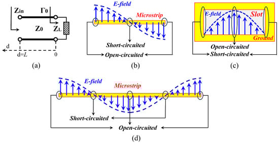
Figure 1.
(a) Transmission line model: the electric field distribution and circuit characteristics of the half-wavelength (b) microstrip line resonators, (c) slot resonators, and (d) one-wavelength microstrip line resonators.
Microstrip line resonators and slot resonators are investigated for their inherent open-circuit and short-circuit characteristics, which are leveraged to introduce notched bands at specific frequency ranges. Figure 1b–d illustrate the electric field distributions and equivalent circuit characteristics of a half-wavelength microstrip line resonator, a half-wavelength slot resonator, and a one-wavelength microstrip line resonator, respectively. For the half-wavelength microstrip line resonator, the electric field reaches its maximum at both ends, representing an open-circuit (high-impedance) condition, and drops to zero at the center, indicating a short-circuit (zero-impedance) condition. In contrast, the half-wavelength slot resonator exhibits zero electric field intensity at both ends (short-circuited behavior) and a peak at the center (open-circuited behavior). The one-wavelength microstrip line resonator presents open-circuit characteristics (high impedance) at both ends and the center while exhibiting short-circuit conditions (zero impedance) at the quarter-wavelength and three-quarter-wavelength positions. Based on these open-/short-circuited conditions, when a transmission signal passes through these resonant structures at their resonant frequencies, significant impedance mismatches occur, resulting in strong signal suppression and the formation of a notched band.
2.2. Evolution of the Proposed UWB Antenna
To clearly demonstrate the design methodology of the proposed ultra-wideband (UWB) antenna with triple-band-notched characteristics, Figure 2 presents four reference antennas along with their voltage standing wave ratio (VSWR) performance. The design process is summarized as follows: First, the baseline antenna, referred to as Ant. I, employs an elliptical patch as the radiating element and is excited through a coplanar waveguide (CPW) feed. The ground plane is chamfered to enhance impedance matching. This antenna achieves a VSWR below 2 across the frequency range of 0.78 GHz to 6.59 GHz. In Ant. II, the upper contour of the elliptical patch is reshaped into a right-angled profile to accommodate a C-shaped slot, which introduces the first notched band, effectively covering 1.02–1.68 GHz. Ant. III incorporates two oppositely oriented U-shaped slots etched beneath the existing C-shaped slot, resulting in the second notched band spanning 2.57–2.72 GHz. Finally, in Ant. IV, a C-shaped microstrip line resonator is loaded on the backside of the dielectric substrate, producing the third notched band within 3.39–3.77 GHz. Through this step-by-step evolution, a UWB antenna with triple-band-notch functionality is successfully realized.
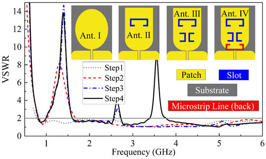
Figure 2.
Four reference antennas and their VSWR performance.
2.3. Analysis of Equivalent Circuit and
To further elucidate the band-notch mechanism of the proposed antenna (Ant. IV), an equivalent circuit model of the ultra-wideband (UWB) antenna is analyzed, as illustrated in Figure 3a. The broadband impedance matching of the UWB antenna can be interpreted as the superposition of multiple adjacent resonant elements, each of which can be modeled by a parallel resonant circuit [14]. The half-wavelength slot structure is equivalently modeled by two parallel-series and resonant circuits, whereas the one-wavelength microstrip line resonator is represented by a parallel-series resonant circuit. The corresponding impedance model is shown in Figure 3b, where the slot resonator behaves as a parallel short-circuit branch, and the microstrip line resonator is modeled as a series short-circuit branch [33]. In this model, denotes the antenna’s radiation resistance. When the antenna operates outside the notched resonance frequencies (i.e., in an open-circuit state), the three resonant branches exert minimal influence on the input signal, which can then propagate efficiently to the load for radiation.
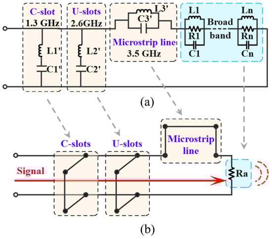
Figure 3.
(a) Equivalent circuits of UWB antenna; (b) impedance model of antenna at passband.
(1) and : Figure 4a,d depict the electric field distribution, the equivalent impedance model, and the signal flow of the antenna at the frequency of 1.3 GHz (). At this frequency, when the C-shaped slot is in resonance, the electric field is predominantly concentrated in the central region of the slot, while the electric field amplitudes at both ends approach zero. This results in the input impedance at the feed point dropping to zero (i.e., a short-circuit condition), causing complete reflection of the incident electromagnetic energy. Moreover, the operational principle of is analogous to that of . The electric field distribution and the corresponding equivalent circuit are shown in Figure 4b,e. These observations suggest that the resonance characteristics of are similar to those of , and their frequency can be expressed as
where c denotes the speed of light in free space, is the total length of the C-/U-shaped slot, and represents the effective dielectric constant. It is important to note that corresponds to half the guided wavelength at the notched frequency .
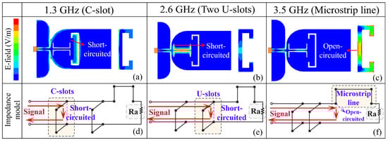
Figure 4.
The electric field distribution at (a) 1.3 GHz, (b) 2.6 GHz, (c) 3.5 GHz; equivalent impedance model and signal flow of the antenna at (d) 1.3 GHz, (e) 2.6 GHz, (f) 3.5 GHz.
(2) : Figure 4c,f illustrate the electric field distribution, equivalent impedance model, and signal flow of the antenna at 3.5 GHz. When the microstrip line resonator is excited at its resonant frequency, the electric field is primarily concentrated along the resonator, with peak values appearing at the center and both ends, as shown in Figure 1d. At this point, the input impedance at the feed location becomes extremely high (in simulation, it exceeds 500 ; for simplicity, it is not explicitly shown). As a result, the incident energy is effectively blocked, leading to the formation of the third notched frequency . The notched frequency can be expressed as
where denotes the total length of the microstrip line. It corresponds to one guided wavelength at the third notched frequency .
2.4. Parametric Studies
A systematic study was conducted on the influence of the total lengths of the three band-notch structures on their respective notch frequencies. As shown in Figure 5a, when the total length of the C-shaped slot varies from 84 mm to 91.5 mm, with the second and third notch frequencies held constant, the first notch frequency shifts significantly toward lower frequencies, demonstrating its dominant role in controlling this notch band. Figure 5b illustrates that as the total length of the U-shaped slot increases from 64.6 mm to 68.6 mm, while the first and third notch frequencies remain unchanged, the second notch frequency also exhibits a downward frequency shift. Meanwhile, variations in the parameter have slight effects on impedance matching around 5 GHz, which requires proper adjustment to optimize antenna performance. As shown in Figure 5c, the total length of the C-shaped microstrip line has a pronounced impact on the third notch frequency. With increasing , the third notch frequency clearly shifts toward lower frequencies, while the first two notch frequencies remain largely unaffected. This indicates the structure enables the independent tuning of specific notch bands.
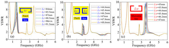
Figure 5.
Effect of (a) , (b) , and (c) on band-notched frequency.
3. Simulation and Measurement Results of the Element
3.1. Antenna Prototype and Reflection Coefficient
To validate the performance of the proposed UWB antenna, a prototype incorporating triple-band-notched structures was fabricated. The detailed dimensions of the UWB antenna are provided in Table 1. Photographs of both the simulated and fabricated antennas are shown in Figure 6. The antenna’s reflection coefficient was measured using a vector network analyzer. As depicted in Figure 7, the measured impedance bandwidths with dB are 0.85–1.02 GHz, 1.59–2.50 GHz, 2.70–3.29 GHz, and 3.66–7.00 GHz. The three notched bands are 1.02–1.59 GHz, 2.50–2.70 GHz, and 3.29–3.66 GHz, which show good agreement with the simulated results.

Table 1.
The detailed dimensions of the proposed UWB antenna (unit: mm).
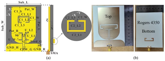
Figure 6.
(a) Simulated and (b) fabricated antenna configurations.
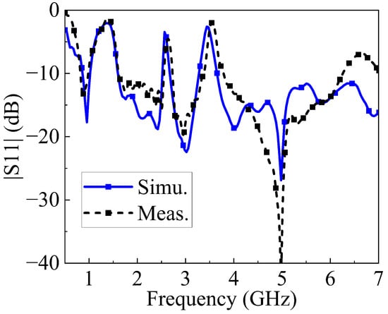
Figure 7.
Simulated and measured reflection coefficients.
3.2. Gain and Efficiency
Figure 8 presents the results for peak realized gain and efficiency. The measured gain shows excellent agreement with the simulation results. It can be observed that the peak gain in the medium and high-frequency ranges remains stable, exceeding 4 dBi. However, at the three notch frequencies, the gain drops to approximately −2 dBi. Meanwhile, the efficiency within the passband is consistently greater than 80%, while it significantly decreases at the three notch frequencies.
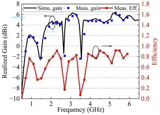
Figure 8.
Simulated and measured peak realized gain and efficiency.
3.3. Radiation Pattern
Figure 9 illustrates the simulated three-dimensional radiation pattern at seven specific frequency points. Among these, three frequencies, 1.2 GHz, 2.5 GHz, and 3.4 GHz, are located near the notch frequency bands. At frequencies of 0.9 and 1.2 GHz, the radiation pattern demonstrates ideal omnidirectional characteristics. At 2.1 GHz, 2.5 GHz, 3.1 GHz, 3.4 GHz, and 5.1 GHz, the presence of higher-order modes causes varying degrees of distortion in the radiation pattern. This distortion can be mitigated by adjusting the current distribution corresponding to these higher-order modes. The results indicate that the directional pattern near the notch frequencies remains unaffected by the notch structure. Figure 10 shows the measured two-dimensional radiation pattern at 0.9, 2.1, 3.1, and 5.1 GHz. Notably, on the YOZ plane, the proposed UWB antenna exhibits excellent omnidirectional radiation characteristics, making it well-suited for UWB communication systems.
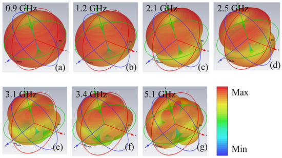
Figure 9.
Simulated 3D radiation patterns of UWB antenna at (a) 0.9, (b) 1.2, (c) 2.1, (d) 2.5, (e) 3.1, (f) 3.4, (g) 5.1 GHz.
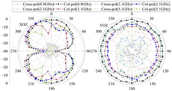
Figure 10.
Measured patterns of UWB antenna at 0.9, 2.1, 3.1, 5.1 GHz.
4. Highly Isolated 2 × 1 MIMO Array Design
Here, this section presents the design methodology of a triple-band-notch UWB MIMO antenna array, coupling suppression strategies.
4.1. Analysis of Element Rotation
As illustrated in Figure 8, two antenna elements are arranged in a face-to-face configuration with a bottom-edge spacing of 112 mm. Without employing any additional decoupling structures, the mutual coupling behavior between the antennas was investigated under various deflection angles. Figure 11a,b show four placement configurations (Cases 1–4) and their corresponding S-parameter results, respectively. In Case 1, the antennas are placed face-to-face in a forward-facing configuration, with both deflection angles and set to 90°. Under this setup, significant mutual coupling is observed, particularly at 0.8 GHz, where the coupling coefficient reaches −11.6 dB, indicating strong inter-element coupling. In Case 2 through Case 4, the antennas are placed vertically in a face-to-face arrangement. In Case 2, the antennas are positioned close to each other, and, despite the vertical orientation, mutual coupling remains high. Note that in Case 2, the bottom spacing between the two antennas is extended to 129 mm to ensure that reaches 180 degrees. However, in Case 3 and Case 4, the antenna spacing is significantly increased compared to Case 1, and, combined with the vertical placement, this effectively suppresses mutual coupling. Simulation results show that both configurations achieve better than 20 dB isolation across the operating band, which is approximately 8.4 dB higher than that in Case 1. The decoupling method with in isolation achieved through the physical rotation of elements is universally applicable to UWB antennas of different shapes. Finally, the configuration from Case 3 was ultimately selected for fabrication and measurement of the 2 × 1 MIMO antenna array. It is evident that the mutual coupling at the three resonant frequencies is extremely low. This phenomenon arises from the fact that the three notched structures reflect signals back to the ports, thereby preventing effective radiation.
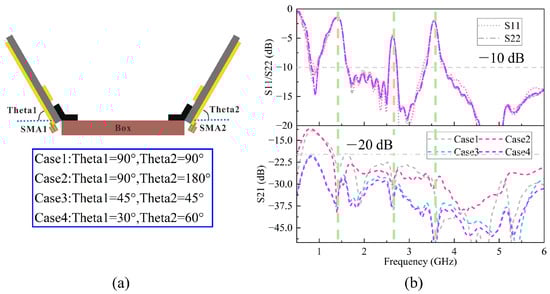
Figure 11.
(a) Four cases with different deflection angles and (b) their performance.
4.2. Effect of Element Spacing
In Case 3, the influence of the distance between the elements on the mutual coupling was investigated, as shown in Figure 12. It can be clearly observed that, as the element spacing increases, the mutual coupling value decreases. Furthermore, the mutual coupling at high frequencies is significantly lower than that at low frequencies. This is because, compared to high frequencies, the wavelength at low frequencies is relatively larger.
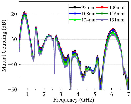
Figure 12.
Mutual coupling between different units at different distances.
5. The 2 × 1 MIMO Experiments and Discussion
5.1. Antenna Prototype and Reflection Coefficient
A prototype of Case 3 was fabricated and characterized. The fabricated antenna is shown in Figure 13, where 3D-printed material was used to support the placement of the two antenna elements. The measured scattering parameters are presented in Figure 14. For Antenna 1, the dB impedance bandwidths are 0.82–1.02 GHz, 1.57–2.50 GHz, 2.68–3.29 GHz, and 3.66–7.00 GHz, with notched frequencies observed at 1.38, 2.56, and 3.44 GHz. Throughout the entire passband, the mutual coupling remains below −24.6 dB, indicating that the mutual coupling between the antennas is significantly suppressed. At the three notched frequencies, the mutual coupling shows the corresponding decoupling nulls. The significant improvement in isolation is attributed to the fact that the antenna cannot radiate normally at these frequencies. Minor differences in the amplitude of the reflection coefficient are observed, which may be due to fabrication errors, measurement setup issues (such as the coaxial line used), and soldering inaccuracies.
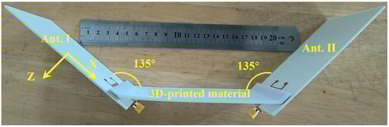
Figure 13.
Fabricated antenna configuration.
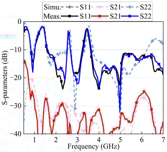
Figure 14.
Simulated and measured S-parameters of MIMO array.
5.2. Envelope Correlation Coefficient (ECC)
In MIMO systems, the ECC (channel correlation coefficient) is a key metric for assessing the similarity of channel characteristics between different antenna elements. A lower ECC value indicates a higher degree of channel independence, which allows MIMO to fully exploit the benefits of spatial diversity and spatial multiplexing. Ideally, the ECC value should be zero. The ECC can be calculated using Equation (4).
Here, and represent port numbers. Figure 15 shows the ECC data from both simulation and measurement. It can be observed that the measured ECC value obtained is less than 0.02 within the passband.
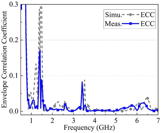
Figure 15.
Simulated and measured ECC of MIMO array.
5.3. Diversity Gain (DG)
In MIMO systems, the primary significance of diversity gain is to mitigate the random fading of wireless channels, thereby enhancing the reliability and stability of link transmission. The ideal value is 10. It can be calculated using the following formula:
The ECC values calculated from Figure 16 are used to compute the DG. Within the passband, both the simulation and test results are close to 10. However, at the first notch frequency band, the DG value drops to 8.7. Overall, the test results are in good agreement with the simulation results.
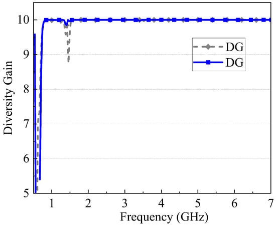
Figure 16.
Simulated and measured DG of MIMO array.
5.4. Total Active Reflection Coefficient (TARC)
In MIMO systems, the core significance of the total active reflection coefficient (TARC) is to quantify the overall impedance matching performance of a multi-antenna array under practical operating conditions. It directly affects the signal transmission efficiency, reception sensitivity, and inter-antenna interference level of MIMO systems, making it a crucial indicator for evaluating the effectiveness of multi-antenna designs. For a two-element MIMO system, TARC can be calculated using S11, S12, S21, and S22. The following formula can be used for estimation:
Figure 17 shows the corresponding TARC values for ranging from 0 to 180 degrees, with a step size of 30 degrees. At different phases, the TARC values exhibit convergence with minor variations.
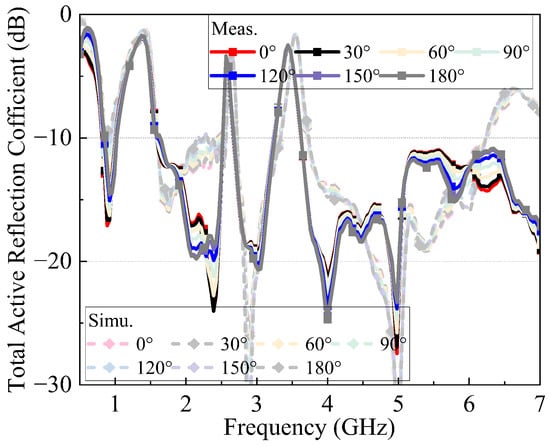
Figure 17.
Simulated and measured TARC of MIMO array.
5.5. Mean Effective Gain (MEG)
In MIMO systems, the core significance of the mean effective gain (MEG) is to quantify the effective signal reception/transmission capability of a single antenna under practical propagation environments. It can be expressed by the following formula:
As shown in Figure 18, throughout the entire passband, both the simulation and test results are close to −3 dB, with a noticeable decrease at the three notch frequency bands. The simulated MEG difference is nearly zero, whereas the measured MEG difference exhibits significant variations only at the notched frequency bands. This discrepancy may be attributed to fabrication errors.
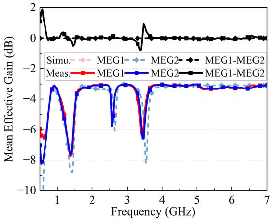
Figure 18.
Simulated and measured MEGs of MIMO array.
5.6. Channel Capacity Loss (CCL)
In MIMO systems, the primary significance of channel capacity loss (CCL) is to quantify the extent to which deviations between practical and ideal channel conditions degrade the maximum transmission capability of the system. It can be expressed using the following formulas:
The expected value of the CCL is less than 0.4 Bits/Sec/Hz. Figure 19 shows the simulated and measured CCL results. Within the passband, its value is less than 0.3 Bits/Sec/Hz. At the three notch frequencies, the values of CCL are as high as 3.11, 1.78, and 2.36 Bits/Sec/Hz, respectively.
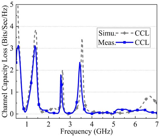
Figure 19.
Simulated and measured CCL of MIMO array.
5.7. Gain and Percentage Efficiency
Since both antenna structures are identical and symmetrically positioned, only element 1 was tested. The measured gain shows good agreement with the simulation results, as shown in Figure 20, with a significant decrease in gain at the three notch frequencies. Similarly, the measured efficiency also exhibits a notable drop at the three notch frequencies.
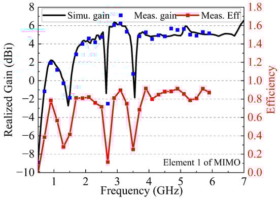
Figure 20.
Simulated and measured realized gain and efficiency of MIMO array.
5.8. Radiation Patterns
Figure 21 presents the three-dimensional radiation patterns at frequencies of 0.9, 1.2, 2.1, 2.5, 3.1, 3.4, and 5.1 GHz, which are consistent with the previously presented simulated unit radiation patterns. This consistency is due to the higher-order modes at higher frequencies, which cause some distortion in the radiation pattern. Such distortion can be mitigated by adding structures like slots to modify the current distribution. Figure 22 shows the measured two-dimensional radiation pattern, where, on the YOZ plane, it exhibits excellent omnidirectional characteristics.
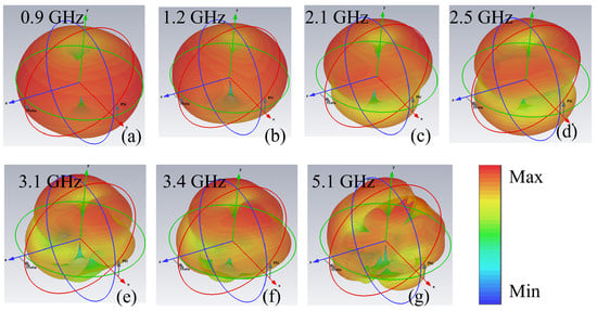
Figure 21.
Simulated 3D radiation patterns of element 1 at (a) 0.9, (b) 1.2, (c) 2.1, (d) 2.5, (e) 3.1, (f) 3.4, (g) 5.1 GHz.
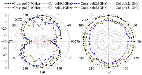
Figure 22.
Measured gain of element 1 at 0.9, 2.1, 3.1, 5.1 GHz.
5.9. Comparisons
Table 2 presents a comparison of the key parameters of the antenna proposed in this work with those of previous studies. It can be observed that the antenna proposed in this work has the following advantages:
Table 2.
Comparison among the proposed antenna with previous methods.
- The proposed antenna features a wide impedance bandwidth.
- It exhibits triple-band notch characteristics, effectively mitigating interference from other applications.
- High isolation is achieved without any decoupling structures, and the self-decoupling method based on element rotation is applicable to UWB antennas of various shapes.
- It demonstrates excellent diversity performance parameters.
6. Conclusions
This paper presents the design, analysis, and experimental validation of a UWB antenna incorporating three distinct notch structures. By integrating a C-shaped slot, two U-shaped slots, and a C-shaped microstrip into the antenna element, three independently tunable notch bands are achieved. The notch mechanisms are thoroughly investigated from both the structural evolution and equivalent circuit modeling perspectives. Building upon the optimized single antenna unit, a 2 × 1 multiple-input, multiple-output (MIMO) antenna array with a face-to-face layout was developed, achieving high inter-element isolation. Across the entire operational bandwidth, the MIMO array exhibits mutual coupling levels better than −24.6 dB. The measured S-parameters closely match the simulated results, confirming the accuracy and feasibility of the proposed design.
Author Contributions
Conceptualization, J.L.; methodology, J.L.; software, J.L. and X.Y.; validation, J.L. and X.Y.; formal analysis, J.L. and F.W.; investigation, J.L. and J.W.; resources, F.W. and Q.Y.; data curation, J.L. and J.W.; writing—original draft preparation, J.L. and Q.Y.; writing—review and editing, J.L., F.W., and Q.Y.; visualization, J.L.; supervision, J.L. and F.W.; project administration, J.L. and F.W.; funding acquisition, F.W. and Q.Y. All authors have read and agreed to the published version of the manuscript.
Funding
This research was supported by the National Natural Science Foundation of China (grant No. 62471128) and Fundamental Research Funds for the Central Universities (2242025F10006 and 2242025RCB0006).
Data Availability Statement
Data is contained within the article.
Conflicts of Interest
The authors declare no conflicts of interest.
Abbreviations
The following abbreviations are used in this manuscript:
| MIMO | Multiple-Input, Multiple-Output |
| UWB | Ultra-Wideband |
| R-L-C | Resistor-Inductor-Capacitor |
| ECC | Envelope Correlation Coefficient |
| DG | Diversity Gain |
| TARC | Total Active Reflection Coefficient |
| MEG | Mean Effective Gain |
| CCL | Channel Capacity Loss |
References
- Zhu, F.; Gao, S.; Ho, A.T.; Abd-Alhameed, R.A.; See, C.H.; Brown, T.W.C.; Li, J.; Wei, G.; Xu, J. Multiple Band-Notched UWB Antenna with Band-Rejected Elements Integrated in the Feed Line. IEEE Trans. Antennas Propag. 2013, 61, 3952–3960. [Google Scholar] [CrossRef]
- Gautam, A.K.; Yadav, S.; Kanaujia, B.K. A CPW-Fed Compact UWB Microstrip Antenna. IEEE Antennas Wirel. Propag. Lett. 2013, 12, 151–154. [Google Scholar] [CrossRef]
- Guo, Z.; Tian, H.; Wang, X.; Luo, Q.; Ji, Y. Bandwidth Enhancement of Monopole UWB Antenna with New Slots and EBG Structures. IEEE Antennas Wirel. Propag. Lett. 2013, 12, 1550–1553. [Google Scholar] [CrossRef]
- Tang, M.C.; Shi, T.; Ziolkowski, R.W. Planar Ultrawideband Antennas with Improved Realized Gain Performance. IEEE Trans. Antennas Propag. 2016, 64, 61–69. [Google Scholar] [CrossRef]
- Lin, C.C.; Jin, P.; Ziolkowski, R.W. Single, Dual and Tri-Band-Notched Ultrawideband (UWB) Antennas Using Capacitively Loaded Loop (CLL) Resonators. IEEE Trans. Antennas Propag. 2012, 60, 102–109. [Google Scholar] [CrossRef]
- Wang, S.; Kong, F.; Li, K.; Du, L. A planar triple-band monopole antenna loaded with an arc-shaped defected ground plane for WLAN/WiMAX applications. Int. J. Microw. Wirel. Technol. 2021, 13, 381–389. [Google Scholar] [CrossRef]
- Abdulzahra, D.H.; Alnahwi, F.; Abdullah, A.S.; Al-Yasir, Y.I.A.; Abd-Alhameed, R.A. A Miniaturized Triple-Band Antenna Based on Square Split Ring for IoT Applications. Electronics 2022, 11, 2818. [Google Scholar] [CrossRef]
- Qu, S.w.; Li, J.l.; Xue, Q. A Band-Notched Ultrawideband Printed Monopole Antenna. IEEE Antennas Wirel. Propag. Lett. 2006, 5, 495–498. [Google Scholar] [CrossRef]
- Lee, C.H.; Wu, J.H.; Hsu, C.I.G.; Chan, H.L.; Chen, H.H. Balanced Band-Notched UWB Filtering Circular Patch Antenna with Common-Mode Suppression. IEEE Antennas Wirel. Propag. Lett. 2017, 16, 2812–2815. [Google Scholar] [CrossRef]
- Liu, H.W.; Ku, C.H.; Wang, T.S.; Yang, C.F. Compact Monopole Antenna with Band-Notched Characteristic for UWB Applications. IEEE Antennas Wirel. Propag. Lett. 2010, 9, 397–400. [Google Scholar] [CrossRef]
- Zaker, R.; Ghobadi, C.; Nourinia, J. Novel Modified UWB Planar Monopole Antenna with Variable Frequency Band-Notch Function. IEEE Antennas Wirel. Propag. Lett. 2008, 7, 112–114. [Google Scholar] [CrossRef]
- Kim, K.H.; Cho, Y.J.; Hwang, S.H.; Park, S.O. Band-notched UWB planar monopole antenna with two parasitic patches. Electron. Lett. 2005, 42, 278–280. [Google Scholar] [CrossRef]
- Abbosh, A.; Bialkowski, M.; Mazierska, J.; Jacob, M. A planar UWB antenna with signal rejection capability in the 4–6 GHz band. IEEE Microw. Wirel. Components Lett. 2006, 16, 278–280. [Google Scholar] [CrossRef]
- Chu, Q.X.; Yang, Y.Y. A Compact Ultrawideband Antenna with 3.4/5.5 GHz Dual Band-Notched Characteristics. IEEE Trans. Antennas Propag. 2008, 56, 3637–3644. [Google Scholar] [CrossRef]
- Jiang, W.; Che, W. A Novel UWB Antenna with Dual Notched Bands for WiMAX and WLAN Applications. IEEE Antennas Wirel. Propag. Lett. 2012, 11, 293–296. [Google Scholar] [CrossRef]
- Zaker, R.; Ghobadi, C.; Nourinia, J. Bandwidth Enhancement of Novel Compact Single and Dual Band-Notched Printed Monopole Antenna with a Pair of L-Shaped Slots. IEEE Trans. Antennas Propag. 2009, 57, 3978–3983. [Google Scholar] [CrossRef]
- Li, J.F.; Chu, Q.X.; Li, Z.H.; Xia, X.X. Compact Dual Band-Notched UWB MIMO Antenna with High Isolation. IEEE Trans. Antennas Propag. 2013, 61, 4759–4766. [Google Scholar] [CrossRef]
- Li, W.T.; Hei, Y.Q.; Feng, W.; Shi, X.W. Planar Antenna for 3G/Bluetooth/WiMAX and UWB Applications with Dual Band-Notched Characteristics. IEEE Antennas Wirel. Propag. Lett. 2012, 11, 61–64. [Google Scholar] [CrossRef]
- Sung, Y. UWB Monopole Antenna with Two Notched Bands Based on the Folded Stepped Impedance Resonator. IEEE Antennas Wirel. Propag. Lett. 2012, 11, 500–502. [Google Scholar] [CrossRef]
- Sarkar, D.; Srivastava, K.V.; Saurav, K. A Compact Microstrip-Fed Triple Band-Notched UWB Monopole Antenna. IEEE Antennas Wirel. Propag. Lett. 2014, 13, 396–399. [Google Scholar] [CrossRef]
- Cai, Y.Z.; Yang, H.C.; Cai, L.Y. Wideband Monopole Antenna with Three Band-Notched Characteristics. IEEE Antennas Wirel. Propag. Lett. 2014, 13, 607–610. [Google Scholar] [CrossRef]
- Vendik, I.B.; Rusakov, A.; Kanjanasit, K.; Hong, J.; Filonov, D. Ultrawideband (UWB) Planar Antenna with Single-, Dual-, and Triple-Band Notched Characteristic Based on Electric Ring Resonator. IEEE Antennas Wirel. Propag. Lett. 2017, 16, 1597–1600. [Google Scholar] [CrossRef]
- Sung, Y. Triple Band-Notched UWB Planar Monopole Antenna Using a Modified H-Shaped Resonator. IEEE Trans. Antennas Propag. 2013, 61, 953–957. [Google Scholar] [CrossRef]
- Srivastava, G.; Mohan, A. Compact MIMO Slot Antenna for UWB Applications. IEEE Antennas Wirel. Propag. Lett. 2016, 15, 1057–1060. [Google Scholar] [CrossRef]
- Ren, J.; Hu, W.; Yin, Y.; Fan, R. Compact Printed MIMO Antenna for UWB Applications. IEEE Antennas Wirel. Propag. Lett. 2014, 13, 1517–1520. [Google Scholar] [CrossRef]
- Liu, L.; Cheung, S.W.; Yuk, T.I. Compact MIMO Antenna for Portable UWB Applications with Band-Notched Characteristic. IEEE Trans. Antennas Propag. 2015, 63, 1917–1924. [Google Scholar] [CrossRef]
- Li, Z.; Yin, C.; Zhu, X. Compact UWB MIMO Vivaldi Antenna with Dual Band-Notched Characteristics. IEEE Access 2019, 7, 38696–38701. [Google Scholar] [CrossRef]
- Jiang, Z.H.; Zhang, L.; Zhang, Y.; Yu, C.; Cai, L.; Zheng, S.; Hong, W. A Compact Triple-Band Antenna with a Notched Ultra-Wideband and Its MIMO Array. IEEE Trans. Antennas Propag. 2018, 66, 7021–7031. [Google Scholar] [CrossRef]
- Kang, L.; Li, H.; Wang, X.; Shi, X. Compact Offset Microstrip-Fed MIMO Antenna for Band-Notched UWB Applications. IEEE Antennas Wirel. Propag. Lett. 2015, 14, 1754–1757. [Google Scholar] [CrossRef]
- Kumari, P.; Gangwar, R.K.; Chaudhary, R.K. An Aperture-Coupled Stepped Dielectric Resonator UWB MIMO Antenna with AMC. IEEE Antennas Wirel. Propag. Lett. 2022, 21, 2040–2044. [Google Scholar] [CrossRef]
- Khan, M.S.; Capobianco, A.D.; Asif, S.M.; Anagnostou, D.E.; Shubair, R.M.; Braaten, B.D. A Compact CSRR-Enabled UWB Diversity Antenna. IEEE Antennas Wirel. Propag. Lett. 2017, 16, 808–812. [Google Scholar] [CrossRef]
- Bazil Taha Ahmed, I.F.R. Compact high isolation UWB MIMO antennas. Wirel. Netw. 2000, 28, 1977–1999. [Google Scholar] [CrossRef]
- Lee, W.S.; Kim, D.Z.; Kim, K.J.; Yu, J.W. Wideband planar monopole antennas with dual band-notched characteristics. IEEE Trans. Microw. Theory Tech. 2006, 54, 2800–2806. [Google Scholar] [CrossRef]
- Khandekar, R.; Sipal, D. Design and Analysis of mm-Wave MIMO Antenna with a UWB AMC. IEEE Antennas Wirel. Propag. Lett. 2025, 24, 2944–2948. [Google Scholar] [CrossRef]
- Li, Y.; Feng, Q. Ultra-Wideband Conformal MIMO Antenna with Ferrite-Based Modified Inverted-F Structure for Wireless Capsule Endoscopy Applications. IEEE Antennas Wirel. Propag. Lett. 2025, 24, 2854–2858. [Google Scholar] [CrossRef]
- Li, K.; Zhang, Y.; Li, Y. Hepta-Mode Terminal Microstrip Antenna for Mobile Wi-Fi 6/6E and UWB Channels 5–11 MIMO Applications. IEEE Trans. Antennas Propag. 2024, 72, 7048–7056. [Google Scholar] [CrossRef]
- Yao, Y.; Shao, Y.; Zhang, J.; Zhang, J. A Transparent Antenna Using Metal Mesh for UWB MIMO Applications. IEEE Trans. Antennas Propag. 2023, 71, 3836–3844. [Google Scholar] [CrossRef]
- Feng, W.; Che, W. Novel Wideband Differential Bandpass Filters Based on T-Shaped Structure. IEEE Trans. Microw. Theory Tech. 2012, 60, 1560–1568. [Google Scholar] [CrossRef]
- Zhang, Y.; Zhang, X.Y.; Pan, Y.M. Low-Profile Planar Filtering Dipole Antenna with Omnidirectional Radiation Pattern. IEEE Trans. Antennas Propag. 2018, 66, 1124–1132. [Google Scholar] [CrossRef]
- Tighilt, Y.; Bensid, C.; Sayad, D.; Mekki, S.; Zegadi, R.; Bouknia, M.L.; Elfergani, I.; Singh, P.; Rodriguez, J.; Zebiri, C. Low-Profile UWB-MIMO Antenna System with Enhanced Isolation Using Parasitic Elements and Metamaterial Integration. Electronics 2023, 12, 4852. [Google Scholar] [CrossRef]
- Kiani, S.H.; Savci, H.S.; Munir, M.E.; Sedik, A.; Mostafa, H. An Ultra-Wide Band MIMO Antenna System with Enhanced Isolation for Microwave Imaging Applications. Micromachines 2023, 14, 1732. [Google Scholar] [CrossRef] [PubMed]
- Altaf, A.; Iqbal, A.; Smida, A.; Smida, J.; Althuwayb, A.A.; Hassan Kiani, S.; Alibakhshikenari, M.; Falcone, F.; Limiti, E. Isolation Improvement in UWB-MIMO Antenna System Using Slotted Stub. Electronics 2020, 9, 1582. [Google Scholar] [CrossRef]


Disclaimer/Publisher’s Note: The statements, opinions and data contained in all publications are solely those of the individual author(s) and contributor(s) and not of MDPI and/or the editor(s). MDPI and/or the editor(s) disclaim responsibility for any injury to people or property resulting from any ideas, methods, instructions or products referred to in the content. |
© 2025 by the authors. Licensee MDPI, Basel, Switzerland. This article is an open access article distributed under the terms and conditions of the Creative Commons Attribution (CC BY) license (https://creativecommons.org/licenses/by/4.0/).