Abstract
To suppress the thermal stress in high-power semiconductor laser array packaging, the classic asymmetric heat dissipation structure of the array packaging was transformed into a symmetric one by incorporating microchannel heat sinks. This effectively reduced the maximum temperature, maximum thermal stress, thermal resistance, and maximum vertical displacement of the semiconductor laser array. Using the response surface methodology, mathematical models were established to correlate the maximum temperature, maximum thermal stress, and maximum vertical displacement of the semiconductor laser array with the radius, height, and spacing of circular micro-pin fins. A genetic algorithm was then employed to perform multi-objective optimization of these parameters. The results demonstrate that, compared to the original packaging configuration, the optimized semiconductor laser array exhibits a maximum temperature reduction of 16.56 °C, a maximum thermal stress decrease of 24.01 MPa, and a reduction in the maximum vertical displacement of the chip by 0.77 μm.
1. Introduction
High-power semiconductor lasers are extensively utilized in industrial applications such as laser cutting, welding, and marking, requiring stable high-power output. Stacked array packaging represents a critical technical approach for achieving high-power semiconductor lasers, significantly enhancing output power [1]. However, high-power operation inevitably generates substantial waste heat, elevating device temperatures and consequently degrading the output power, wavelength stability, and reliability [2]. Research indicates that the optimal junction temperature for laser operation should remain below 40 °C, with the maximum operational temperature not exceeding 60 °C [3,4]. Significant mismatches in the coefficients of thermal expansion (CTE) between semiconductor laser materials and their packaging substrates generate thermal stresses when temperature fluctuates, owing to differential expansion and contraction [5]. This stress not only accelerates device degradation and reliability reduction but also causes substantial displacement of bar chips along the fast-axis direction [6]. Consequently, the near-field laser output exhibits pronounced nonlinear distribution in this orientation [7,8]. Such nonlinear effects severely constrain beam collimation, shaping, beam combining, and fiber-coupling efficiency, emerging as critical bottlenecks for device performance and application viability [9,10]. Therefore, developing effective thermal management solutions for high-power semiconductor laser arrays is imperative.
Currently, researchers have conducted in-depth studies on the thermal stress in bar packaging through theoretical analysis, simulation, and experimental validation. In 2009, Chaparala et al. [11] investigated the thermal stress and deformation in semiconductor laser packaging caused by CTE mismatch. In 2015, Anna et al. [12] introduced glass microchannels into copper cooler channels, reducing the cooler’s dimension perpendicular to the junction plane, providing a reference for cooling high-power laser arrays. In 2020, Zhen Wu [13] simulated the influence of beam positional and directional errors on spectral beam combining output. The results indicated that directional errors in the fast and slow axes have a greater impact on the output beam quality. In 2022, Gordeev et al. [14] compared the thermal stress of bars assembled on CuW and AlN substrates, revealing significant differences in the maximum thermal stress of laser arrays on different substrate materials. Most current studies focus on the temperature rise, thermal stress, and chip displacement of individual bars, while fewer address the operational state of microchannel water-cooled semiconductor laser arrays.
Accordingly, this study investigates the thermo-mechanical response of semiconductor laser arrays packaged with microchannel heatsinks. A three-dimensional model of the microchannel heatsink-packaged laser stack was developed to comprehensively evaluate the temperature distribution, thermal stress fields, and vertical chip displacement under actual operating conditions through numerical simulation. Symmetrically packaged microchannel heatsinks were implemented to enhance the thermal dissipation capacity of the semiconductor laser arrays. Building upon this foundation, the Box–Behnken Design (BBD) methodology was systematically employed to examine the influence of key geometric parameters (radius, height, spacing) of the micro-pin fins on microchannel heatsink performance. Furthermore, a multi-objective optimization framework integrating a Genetic Algorithm (GA) and Response Surface Methodology (RSM) was implemented to globally optimize micro-pin fin structural parameters. This approach concurrently minimizes the maximum temperature, peak thermal stress, and maximum chip vertical displacement, aiming to achieve a comprehensive optimal heatsink design that improves thermal efficiency, device reliability, and beam quality. Collectively, this research provides a novel approach to addressing thermal stress and beam nonlinear distribution challenges in stacked laser arrays.
2. Numerical Models and Theoretical Analysis
2.1. Physical Geometric Model
A single microchannel water-cooled packaged semiconductor laser bar is shown in Figure 1, which consists of a micro-channel cooling (MCC) heat sink, solder layer, semiconductor laser bar, insulating film, electrode, and copper foil [2]. The P-side of the bar is soldered onto the heat sink. The microchannel heat sink is fabricated by welding five layers of oxygen-free high-conductivity copper, with dimensions of 27 mm × 10.8 mm × 1.5 mm. The semiconductor laser bar emits at a wavelength of 808 nm, with a cavity length of 1 mm, a fill factor of 30%, and a total of 19 emission points. The operating power of a single bar is 60 W, and due to an electro-optical conversion efficiency of 60%, the thermal load during operation is 40 W. To achieve higher laser output power, multiple MCC-packaged semiconductor laser bars are typically stacked along the fast-axis direction to form a semiconductor laser array, with rubber O-rings used for sealing. Five MCC laser bars are vertically stacked, as shown in Figure 2. The semiconductor laser array employs a parallel cooling circuit with an inlet water velocity of 6 m/s and a temperature of 25 °C for heat dissipation. During operation, heat dissipation in semiconductor laser arrays is primarily achieved through forced cooling via microchannel heatsinks, while radiative heat loss and air convection are considered negligible [15]. Table 1 summarizes the material properties of each layer in the semiconductor laser array, assuming temperature-independent properties.
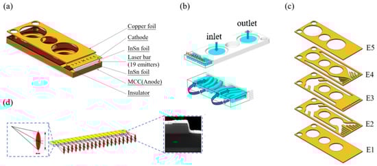
Figure 1.
Schematic diagrams of laser packaging. (a) Schematic diagram of the laser structure; (b) schematic diagram of microchannel heat dissipation; (c) internal structure diagram of the microchannel heat sink; (d) laser bar and its partial enlarged view.
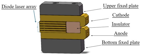
Figure 2.
Schematic diagram of a vertical stacked semiconductor laser array.

Table 1.
Material properties of each layer in the arrayed semiconductor laser package.
2.2. Mesh Independence Verification
To ensure the reliability and stability of the finite element analysis results while optimizing computational costs and balancing accuracy with efficiency, a mesh independence verification was performed on the finite element model of the MCC semiconductor laser array under identical operating conditions. Table 2 presents the numerical solutions for the maximum temperature, maximum thermal stress, and maximum vertical displacement of the chips in the MCC-cooled semiconductor laser array under varying mesh densities. When the mesh count reached 5,097,286, the maximum discrepancy with the benchmark mesh was only 1.55%, with all errors below 2%, satisfying the mesh independence criterion. Considering the mesh quality, the accuracy of the numerical solution, and the computational cost, a mesh count of 5,097,286 was ultimately selected for the semiconductor laser array model.
Table 2.
Simulated package properties vs. mesh count.
2.3. Mathematical Analysis of Heat Generation and Thermal Stress in Semiconductor Lasers
2.3.1. Heat Generation Mechanism in Semiconductor Lasers
Currently, the limited electro-optical conversion efficiency of semiconductors under room-temperature conditions results in significant waste heat generation during operation. A failure to dissipate this heat promptly and effectively leads to a substantial temperature rise in the laser, directly impacting its performance parameters and severely compromising the reliability of semiconductor lasers [16,17]. The heat generated in semiconductor lasers primarily originates from two aspects:
- (1)
- During the normal operation of semiconductor lasers, the injected current causes electrons and holes to recombine in the active region, producing laser emission. This process generates substantial heat due to absorption associated with spontaneous radiation, stimulated radiation, and non-radiative processes. The Joule heating produced in the active region can be expressed as follows [18]:
- (2)
- The Joule heat generated in the non-active region semiconductor materials and Ohmic contact resistance can be expressed as follows [18]:
In the equation, represents the heat power density in the non-active region, and denotes the total resistance in the non-active region.
2.3.2. Theoretical Analysis of Thermal Stress in Semiconductor Lasers
Thermal expansion and contraction are inherent material properties characterized by the CTE. When the temperature changes, inconsistent temperature distribution within the semiconductor laser causes differential displacement among material points or restricts free expansion/contraction due to external constraints. This generates thermal stress within the device. The corresponding elastic thermal strain is given by:
In the equation, represents the CTE of the thin film, and denotes the CTE of the substrate. According to Hooke’s law, the thermal stress is expressed as:
where is the elastic modulus of the thin film, and is Poisson’s ratio.
Semiconductor lasers feature complex structures with multiple material types. To conveniently describe the stress and strain induced by temperature rise during operation, the equivalent stress and equivalent strain—based on the von Mises yield criterion—are used to characterize the internal stress and strain of the laser array. The equivalent stress is expressed as:
The equivalent strain is:
2.3.3. Thermal Resistance in Semiconductor Lasers
Thermal resistance reflects a material’s inherent ability to impede heat transfer. It is a critical parameter for thermal analysis in semiconductor lasers, as it directly reveals the device’s heat dissipation capability and indicates the quality of device packaging. The calculation formula for thermal resistance is as follows [19]:
where represents the operating junction temperature of the semiconductor laser array, denotes its initial temperature, and is the thermal power generated by the semiconductor laser array.
3. Simulation Results and Analysis
3.1. Effect of Symmetric Microchannel Heatsink Packaging on Thermal Stress in Semiconductor Laser Arrays
Semiconductor laser arrays are formed by stacking bars along the fast-axis direction with integrated microchannel heat sinks beneath each bar to mitigate thermal effects, where Figure 2 illustrates a typical five-bar configuration employing five independent microchannel heat sinks. Figure 3a reveals a maximum operational temperature of 56.47 °C localized at the uppermost bar—significantly exceeding optimal laser diode operating temperatures and approaching the upper reliability threshold, thereby compromising long-term operational stability—while a maximum thermal stress of 44.14 MPa concurrently occurs at this position. Subsequently, Figure 3b demonstrates thermally induced vertical displacement perpendicular to the PN junction across all chip layers, designated Chip 1 through Chip 5 from top to bottom, with the bottom-most laser chip exhibiting a maximum displacement of 1.67 μm.
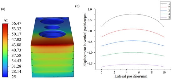
Figure 3.
Temperature rise of typical semiconductor laser stack arrays and displacement distribution of laser chips. (a) Temperature rise; (b) displacement distribution of chips.
In a typical semiconductor laser array configuration, the topmost laser chip dissipates heat solely through a single MCC, while chips at other positions utilize both upper and lower MCCs to remove thermal energy from the bars. Consequently, the temperature rise, thermal stress, and vertical displacement of this top-layer chip exhibit the most pronounced effects. To address this, an additional structurally identical microchannel heat sink was integrated at the uppermost position, creating a symmetric MCC configuration to enhance thermal management capabilities. Figure 4a illustrates the temperature distribution in the symmetrically packaged laser array, revealing maximum thermal metrics at the central bar: a maximum temperature of 43.88 °C, a thermal resistance of 0.47 °C/W, and a maximum thermal stress of 25.35 MPa. Figure 4b displays the vertical displacement across chip layers in this symmetric configuration, with the maximum chip displacement measuring 1.12 μm.
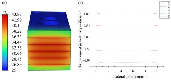
Figure 4.
Thermal and displacement distribution in symmetrically microchannel-cooled semiconductor laser arrays. (a) Temperature rise; (b) displacement distribution of chips.
The comprehensive analysis demonstrates that the symmetrically packaged microchannel heatsink enhances the thermal dissipation capacity of the semiconductor laser array. This results in a 12.59 °C reduction in maximum temperature, a thermal resistance decrease from 1.05 °C/W to 0.47 °C/W representing a 55% improvement, an 18.79 MPa reduction in maximum thermal stress, and a 0.54 μm decrease in maximum vertical chip displacement. These improvements collectively mitigate the temperature rise, thermal stress, and interlayer displacement. Additionally, the maximum temperature difference between chips decreases by 12.34 °C, confirming substantially enhanced cooling uniformity through the novel configuration. However, the operational temperature of the laser array remains above the optimal range, resulting in suboptimal performance conditions.
3.2. Multi-Objective Optimization of Microchannel Heat Sinks
Mutual thermal interference among emitter units in semiconductor laser arrays induces non-uniform heat dissipation. Existing research predominantly focuses on modifying heatsink structures to enhance thermal performance. However, these investigations typically examine single structural parameters’ impacts on heat transfer capacity, employing oversimplified evaluation metrics. This approach disregards the interaction effects between multiple factors, the misleading nature of singular evaluation criteria, and experimental efficiency considerations. Consequently, these limitations prevent substantial improvements in the thermal reliability of laser arrays.
Multi-objective optimization of the microchannel heat sink’s internal structure was achieved by integrating circular micro-pin fins with RSM and genetic algorithms. The primary procedure begins with defining design variables and objective functions. A BBD subsequently performs response surface analysis on these variables. Regression models are then constructed using the data generated by the BBD, followed by statistical validation of their significance through analysis of variance. The optimization process culminates using genetic algorithms to identify Pareto-optimal solutions, thereby determining the optimal parameter combination under specified constraints [20,21]. As a classical response surface methodology, BBD efficiently constructs quadratic polynomial models between factors and responses with minimal experiments, enabling multiphysics relationship analysis and optimal parameter identification.
3.2.1. Design Variables and Objective Functions
The primary objective of multi-objective optimization for microchannel heat sinks is to efficiently dissipate waste heat generated by semiconductor laser arrays, thereby reducing the temperature rise, thermal stress, and chip displacement while enhancing device reliability. Circular micro-pin fins function as discretely implanted cylindrical micro-cooling columns within microchannels, achieving high-efficiency thermal management by enhancing the local turbulent intensity and heat transfer surface area without significantly increasing the pressure drop. Studies demonstrate that the radius R, height H, and spacing B of circular micro-pin fins significantly impact the thermal performance of microchannel heat sinks, as illustrated in Figure 5 [22]. Consequently, these three parameters—radius, height, and spacing—were selected as design variables. The maximum temperature, maximum thermal stress, and maximum vertical chip displacement of the semiconductor laser array served as objective functions. The parametric ranges for R, H, and B were determined based on internal microchannel dimensions and prior research, with optimized parameters listed in Table 3. The values −1, 0, and 1 represent dimensionless coded levels corresponding to the low, center, and high levels of each design variable after standardization.
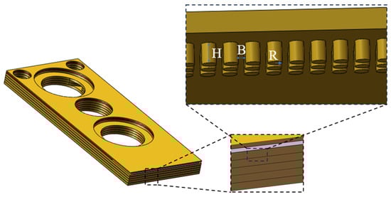
Figure 5.
Schematic diagram of radius, density, and spacing of circular micro-pin fins.
Table 3.
Design variable parameters.
3.2.2. Response Surface Regression Models
RSM is an optimization approach grounded in statistics and experimental design. It quantifies nonlinear relationships between multiple factors and response values through rational experimental design and mathematical modeling with minimal experimental iterations, efficiently analyzes factor interactions, and identifies optimal conditions. Its core components encompass experimental design, model fitting, and variance analysis. Table 4 presents the design matrix and finite element simulation results obtained via the BBD methodology.
Table 4.
Design and results of the BBD scheme.
Based on the BBD experimental design and results presented earlier, the response surface models correlating objective functions—maximum temperature of the semiconductor laser array (Y1), maximum thermal stress (Y2), and maximum vertical chip displacement (Y3)—with design variables R, H, and B were fitted via the least squares method. The mathematical expressions are given by Equations (8)–(10):
Figure 6 shows the predicted and experimental values of the maximum temperature, maximum thermal stress, and maximum vertical displacement of the chips in the semiconductor laser array. All data points distribute near the diagonal line, confirming good consistency between the predicted and experimental values at design points, with maximum errors of 0.32% for temperature, 1.07% for thermal stress, and 0.853% for chip displacement. This demonstrates small prediction errors and an accurate model representation of physical phenomena.
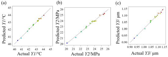
Figure 6.
Comparison between actual values and predicted values in the response surface regression model. (a) Maximum temperature of the semiconductor laser stack array; (b) maximum thermal stress of the semiconductor laser stack array; (c) maximum vertical displacement of the chip.
3.2.3. Response Surface Analysis
In the integrated RSM-GA multi-objective optimization framework, model validation serves as the critical step for ensuring the reliability of response surface models, directly determining the accuracy of subsequent optimization results. Consequently, analysis of variance must be conducted on the response surface models corresponding to the semiconductor laser array’s maximum temperature, maximum thermal stress, and maximum vertical chip displacement.
The ANOVA results for the maximum temperature regression equation (as presented in Supplementary Table S1: Analysis of the maximum temperature model equation) indicate the following: The model term shows a p-value < 0.0001, indicating statistical significance at an extremely high level. The lack-of-fit term yields a p-value = 0.1165 (>0.05), confirming its insignificance. This validates the model’s goodness of fit and establishes the effectiveness of the maximum temperature regression equation. Significant factors influencing the maximum temperature response include R, H, B, RH, RB, HB, R2, H2, and B2. ANOVA results (as shown in Supplementary Tables S2 and S3) confirm the effectiveness of both the maximum thermal stress response surface model and the maximum vertical displacement response surface model. Significant factors for thermal stress comprise R, H, B, R H, R2, H2, and B2, while factors R, H, B, RH, RB, R2, H2, and B2 significantly influence the vertical displacement response.
The reliability analysis (see Supplementary Table S4: Correlation coefficients of the target model) indicates that the closer the model’s correlation coefficient R2 is to 1, the stronger the correlation significance of the response surface model. The R2 values for the semiconductor laser array’s maximum temperature, maximum thermal stress, and maximum vertical chip displacement are 99.31%, 98.68%, and 99.04%, respectively. Differences between R2 (Predicted) and R2 (Adjusted) for these parameters measure 0.0833, 0.1465, and 0.1036, all below 0.2. These results confirm a high model correlation, demonstrating an effective representation of relationships between responses and independent variables. The regression models thus serve as effective mathematical tools for predicting maximum temperature, maximum thermal stress, and maximum vertical chip displacement in semiconductor laser arrays.
3.2.4. Genetic Algorithm Optimization
Building on the established response surface models Y1, Y2, and Y3, GA optimization was applied to minimize the semiconductor laser array’s maximum temperature, maximum thermal stress, and maximum vertical chip displacement. GAs, computational models simulating biological evolution, exhibit robust applicability for nonlinear, non-convex problems with multiple constraints. Through crossover, mutation, and natural selection mechanisms, they iteratively evolve superior approximate solutions. This approach enables a global search within the solution space, effectively avoiding premature convergence to local optima.
The multi-objective optimization model is expressed as follows:
The mathematical formulation defines Y1, Y2, and Y3 as response surface models correlating design variables R, H, and B to the maximum temperature, maximum thermal stress, and maximum vertical chip displacement in the semiconductor laser array. The multi-objective genetic algorithm employed a population size of 100 evolved over 500 generations, with crossover probability fixed at 0.9. Adaptive mutation dynamically balanced global exploration and local exploitation, while retaining 30% of Pareto-optimal solutions. Figure 7 illustrates the uniformly distributed Pareto frontier after 500 generations, confirming algorithmic convergence. Point A corresponds to minimized temperature and vertical displacement, while Point B minimizes thermal stress. Considering the manufacturing difficulty of circular micro-pin fins and the small differences in temperature, thermal stress, and displacement between Points A and B, Point A was selected as the optimal solution. This configuration yields a predicted maximum temperature of 39.66 °C, maximum thermal stress of 19.38 MPa, and maximum vertical displacement of 0.89 μm. The corresponding micro-pin fin parameters are radius R = 0.1 mm, height H = 0.3 mm, and spacing B = 0.1 mm.
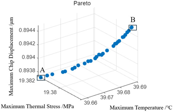
Figure 7.
Changes in the distribution of the Pareto optimal front after 500 iterations.
3.2.5. Simulation Validation
Given the predictive nature of optimization results, simulation verification was performed to confirm the effectiveness of the Pareto-optimal solution. Figure 8a presents the temperature distribution of the optimized semiconductor laser array, indicating a maximum temperature of 39.91 °C with a 0.6% prediction error. The maximum thermal stress measured 20.13 MPa, exhibiting a 3.7% relative error. Figure 8b illustrates the displacement distribution across chip layers under optimal parameters, showing a maximum vertical displacement of 0.90 μm with a 1.1% prediction discrepancy. Compared to conventional packaging configurations, the optimized array demonstrates significant improvements: a 16.56 °C reduction in maximum temperature, a 24.01 MPa decrease in maximum thermal stress, and a 0.77 μm reduction in maximum vertical chip displacement. Post-optimization results maintain the maximum chip temperature below 40 °C, ensuring operation within the optimal thermal range and enhancing reliability under service conditions.
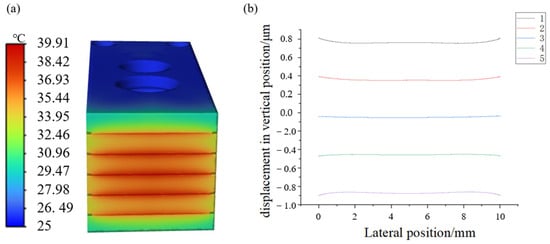
Figure 8.
Temperature rise of semiconductor laser stack arrays and displacement distribution of chips under optimal parameter combination. (a) Temperature rise; (b) displacement distribution of chips.
This study establishes a portable closed-loop design methodology integrating surrogate modeling with multi-objective optimization. The core workflow initiates with constructing high-fidelity quadratic response surface surrogate models using limited initial experimental data to efficiently map complex multiphysics responses. Subsequently, genetic algorithm-driven multi-objective optimization performs global Pareto front exploration within the continuous solution space generated by the surrogate model. The process concludes by validating results through minimal high-confidence solutions for iterative refinement. Maintaining prediction errors strictly below 3.7%, this methodology reduces experimental iterations by over 44% compared to conventional approaches while systematically eliminating the subjective bias inherent in trial-and-error methods.
4. Conclusions
To enhance the thermal reliability of semiconductor laser arrays in service environments, this study establishes a thermo-fluidic-mechanical multiphysics coupling model to numerically evaluate the impact of symmetrically packaged microchannel heatsinks on thermal performance. Concurrently, we propose a transferable closed-loop design methodology integrating surrogate modeling and multi-objective optimization. This approach employs RSM to derive explicit mathematical relationships between circular micro-pin fin structural parameters in microchannel heatsinks and the laser array’s maximum temperature, peak thermal stress, and maximum chip displacement. GA optimization then identifies the optimal parameter combination through multi-objective criteria. Key conclusions are as follows:
- (1)
- Symmetric microchannel packaging significantly enhances the thermal management capacity of semiconductor laser arrays. Transitioning from asymmetric to symmetric microchannel heatsink packaging reduces the peak laser temperature by 12.59 °C, decreases the thermal resistance by 55% (from 1.05 °C/W to 0.47 °C/W), lowers the maximum thermal stress by 18.79 MPa, and reduces the maximum vertical displacement of laser bars by 0.55 μm. Concurrently, the maximum temperature differential between chips decreases by 12.34 °C, demonstrating substantially improved cooling uniformity through symmetric microchannel packaging.
- (2)
- Optimization of circular micro-pin fin structures within the microchannel heatsink was conducted using RSM to establish polynomial regression models between the pin-fin radius (R), height (H), and spacing (B), and the laser array’s maximum temperature, peak thermal stress, and maximum chip displacement. Model goodness-of-fit and reliability were rigorously validated. Genetic Algorithm multi-objective optimization determined the optimal parameter combination as R = 0.1 mm, H = 0.3 mm, and B = 0.1 mm. The predicted results closely align with simulation data, with a maximum error of merely 3.7%.
- (3)
- After optimization, the microchannel heatsink demonstrates significantly enhanced thermal performance, maintaining the semiconductor laser array at an operating temperature of 39.91 °C within the optimal working range. Compared to conventional packaging configurations, the optimized design achieves a 16.56 °C reduction in the peak temperature, a 24.01 MPa decrease in the maximum thermal stress, and a 0.77 μm reduction in the maximum vertical chip displacement, representing a breakthrough advancement in thermal management capabilities.
This study investigates thermal effects in semiconductor laser arrays during operation and proposes strategies to mitigate thermal loading. The findings demonstrate that optimized packaging configurations significantly enhance array reliability under thermal stress conditions. This research provides valuable insights for enhancing the performance stability of semiconductor laser arrays in operational environments.
Supplementary Materials
The following supporting information can be downloaded at: https://www.mdpi.com/article/10.3390/electronics14163336/s1, Table S1: Analysis of the maximum temperature model; Table S2: Variance analysis of the maximum thermal stress model equation; Table S3: Variance analysis of the maximum vertical displacement model; Table S4: Correlation coefficients of the target model.
Author Contributions
Conceptualization, L.C. and B.W.; methodology, L.C.; software, B.W.; validation, L.C. and X.D.; formal analysis, H.S.; investigation, B.W.; resources, L.C.; data curation, X.D.; writing—original draft preparation, B.W.; writing—review and editing, B.W. and L.C.; visualization, Y.B.; supervision, X.D.; project administration, L.C.; funding acquisition, L.C. All authors have read and agreed to the published version of the manuscript.
Funding
This research was supported by the 2022 Shanxi Provincial Major Science and Technology Special Project (NO. 202201030201009); Jincheng Key Research and Development Program (High-tech Field) Project (NO. 20240120).
Data Availability Statement
The original contributions presented in this study are included in the article; further inquiries can be directed to the corresponding authors.
Conflicts of Interest
The authors declare no conflicts of interest.
Abbreviations
The following abbreviations are used in this manuscript:
| CTE | Coefficient of Thermal Expansion |
| BBD | Box–Behnken Design |
| GA | Genetic Algorithm |
| RSM | Response Surface Methodology |
| MCC | Micro-Channel Cooling |
References
- Liu, J.; Wang, M.; Wang, Y.; Zhou, X.; Fu, T.; Qi, A.; Qu, H.; Xing, X.; Zheng, W. High maximum power density and low mechanical stress photonic-band-crystal diode laser array based on non-soldered packaging technology. Chin. Opt. Lett. 2022, 20, 071403. [Google Scholar] [CrossRef]
- Cheng, L.; Sun, H.; Dai, X.; Wei, B. Optimization of Heat-Dissipation Structure of High-Power Diode Laser in Space Environments. Micromachines 2024, 15, 968. [Google Scholar] [CrossRef] [PubMed]
- Zhang, P.; Wang, J.W.; Hou, D.; Wang, Z.F.; Xiong, L.L.; Liu, H.; Nie, Z.Q.; Liu, X.S.; Zhang, P.; Wang, J.; et al. A 3000W 808 Nm QCW G—Stack Semiconductor Laser Array. In Proceedings of the XX International Symposium on High Power Laser Systems and Applications; International Society for Optics and Photonics: Bellingham, WA, USA, 2015; p. 92550W–1-7. [Google Scholar]
- Wu, S.; Li, T.; Wang, Z.; Chen, L.; Zhang, J.; Zhang, J.; Liu, J.; Zhang, Y.; Deng, L. Study of Temperature Effects on the Design of Active Region for 808 nm High-Power Semiconductor Laser. Crystals 2023, 13, 85. [Google Scholar] [CrossRef]
- Hasler, K.; Frevert, C.; Crump, P.; Erbert, G.; Wenzel, H. Numerical study of high-power semiconductor lasers for operation at subzero temperatures. Semicond. Sci. Technol. 2017, 32, 045004. [Google Scholar] [CrossRef]
- Wang, M.P.; Zhang, P.; Nie, Z.Q.; Liu, H.; Sun, Y.B.; Wu, D.H.; Zhao, Y.L. Analysis of Cryogenic Characteristics of High Power Semiconductor Lasers. Acta Phtonica Sin. 2019, 48, 0914002. [Google Scholar] [CrossRef]
- Nie, Z.; Lu, Y.; Chen, T.; Zhang, P.; Wu, D.; Wang, M.; Xiong, L.; Li, X.; Wang, Z.; Liu, X. Thermomechanical Behavior of Conduction-Cooled High-Power Diode Laser Arrays. IEEE Trans. Compon. Pack. Manuf. Technol. 2018, 8, 818–829. [Google Scholar] [CrossRef]
- Lin, C.; Lin, J.; Tai, P.; Wang, T.; Feng, B.; Chou, C.; Han, P. Design and Experimental Study of Wavelength Beam Combining System Using Full-Bar Diode Laser Stacks. IEEE Photonics Technol. Lett. 2024, 36, 535–538. [Google Scholar] [CrossRef]
- Zhang, H.; Hu, Y.; Peng, S.; Liu, Y. The SMILE Effect in the Beam Propagation Direction Affects the Beam Shaping of a Semiconductor Laser Bar Array. Photonics 2024, 11, 161. [Google Scholar] [CrossRef]
- Zhang, Q.; Feng, P.; Yang, C.; Zhuang, Y.; Cai, W.; Wu, Z. Spectral analysis of beam-combining-systems based on laser array with smile effect. Opt. Commun. 2024, 550, 130018. [Google Scholar] [CrossRef]
- Chaparala, S.C.; Hughes, L.C.; Kwak, J. Thermo-Mechanical Analysis of a Laser Diode Chip in an Opto-Electronic Package. In Proceedings of the ASME 2009 InterPACK Conference, San Francisco, CA, USA, 19–23 July 2009. IPACK2009-89108. [Google Scholar]
- Kozlowska, A.; Lapka, P.; Seredynski, M.; Teodorczyk, M.; Dabrowska-Tumanska, E. Experimental study and numerical modeling of micro-channel cooler with micro-pipes for high-power diode laser arrays. Appl. Therm. Eng. 2015, 91, 279–287. [Google Scholar] [CrossRef]
- Wu, Z.; You, S.; Du, Q.; Huang, Y. Influence of smile effect on beam properties of spectrally combined beams based on diode laser stacks. Opt. Commun. 2020, 471, 126031. [Google Scholar] [CrossRef]
- Gordeev, V.; Oleshchenko, V.; Bezotosnyi, V. Thermoelastic stresses in high-power CW diode laser arrays assembled on CuW and AlN submounts. Quantum Electron. 2022, 52, 443. [Google Scholar] [CrossRef]
- Qu, W.; Mudawar, I. Experimental and numerical study of pressure drop and heat transfer in a single-phase micro-channel heat sink. Int. J. Heat Mass Transf. 2002, 45, 2549–2565. [Google Scholar] [CrossRef]
- Jing, H.; Zhong, L.; Ni, Y.; Zhang, J.; Liu, S.; Ma, X. Design and simulation of a novel high-efficiency cooling heat-sink structure using fluid-thermodynamics. J. Semicond. 2015, 36, 37–42. [Google Scholar] [CrossRef]
- Rapp, S.; Piprek, J.; Streubel, K.; Andre, J.; Wallin, J. Temperature sensitivity of 1.54-mu m vertical-cavity lasers with an InP-based Bragg reflector. IEEE J. Quantum Electron. 1997, 33, 1839–1845. [Google Scholar] [CrossRef]
- Camps, I.; Gonzalez, J.; Sanchez, M. Calculation of the thermal resistance and temperature distribution in blue-green semiconductor lasers. Semicond. Sci. Technol. 1997, 12, 1574–1578. [Google Scholar] [CrossRef]
- Choi, J.H.; Shin, M.W. Thermal Analysis of the Open Type of Laser Diode. In Proceedings of the IEEE International Workshop on Thermal Investigations of ICs & Systems, Paris, France, 27–29 September 2011; pp. 1–5. [Google Scholar]
- Tang, Z.; Sun, R.; Lu, K.; Cheng, J.; Zhou, P. Multi-objective optimization of flow boiling heat transfer in a manifold microchannel heat sink with curved corners. Int. J. Heat Mass Transf. 2025, 247, 127182. [Google Scholar] [CrossRef]
- Shao, X.; Marzban, A.; Pourfattah, F.; Akbari, O.; Ahmadi, G.; Emami, N.; Salahshour, S. Optimization of the flow guiding fins configuration and tube arrangements in a shell and tube heat exchanger: Coupling response surface methodology and CFD. Case Stud. Therm. Eng. 2025, 72, 106279. [Google Scholar] [CrossRef]
- Zhang, S.; Wu, J.; Gong, B.; Yu, S.; Qiao, Z.; Liu, Q.; Su, Z.; Sun, J.; Wang, X.; Sun, H. Performance enhancement of cyclone deoiling for oily sludge based on BP neural network model and genetic algorithm. Powder Technol. 2025, 460, 121029. [Google Scholar] [CrossRef]


Disclaimer/Publisher’s Note: The statements, opinions and data contained in all publications are solely those of the individual author(s) and contributor(s) and not of MDPI and/or the editor(s). MDPI and/or the editor(s) disclaim responsibility for any injury to people or property resulting from any ideas, methods, instructions or products referred to in the content. |
© 2025 by the authors. Licensee MDPI, Basel, Switzerland. This article is an open access article distributed under the terms and conditions of the Creative Commons Attribution (CC BY) license (https://creativecommons.org/licenses/by/4.0/).