
Impact of Charge Carrier Trapping at the Ge/Si Interface on Charge Transport in Ge-on-Si Photodetectors

 ,
, 
Abstract
1. Introduction
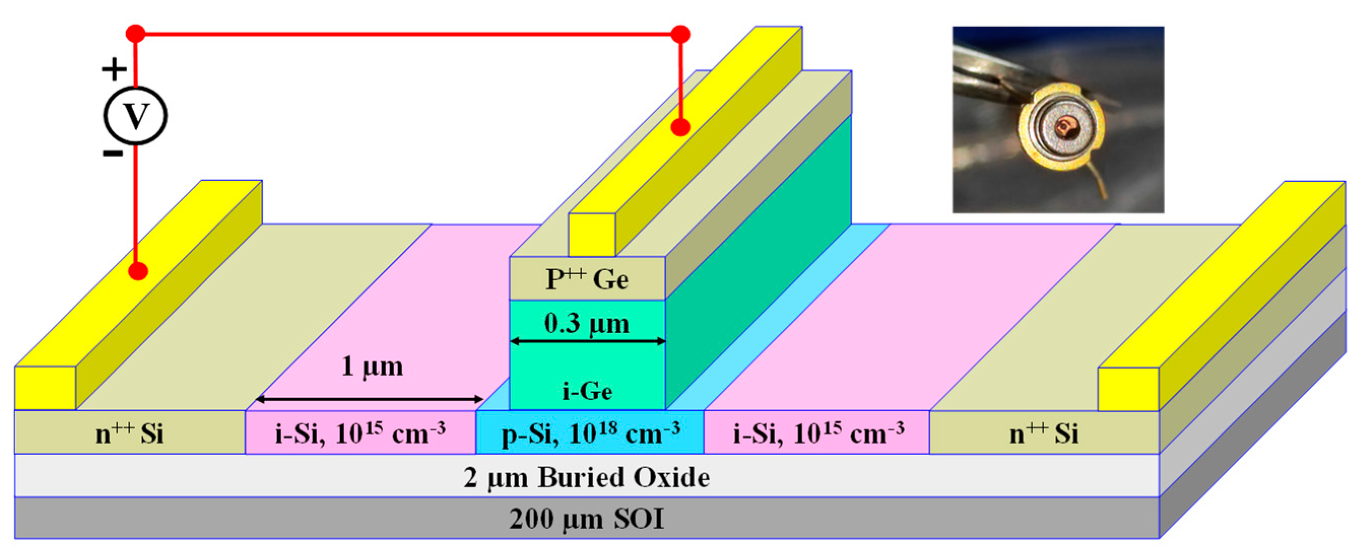
2. Experimental Details
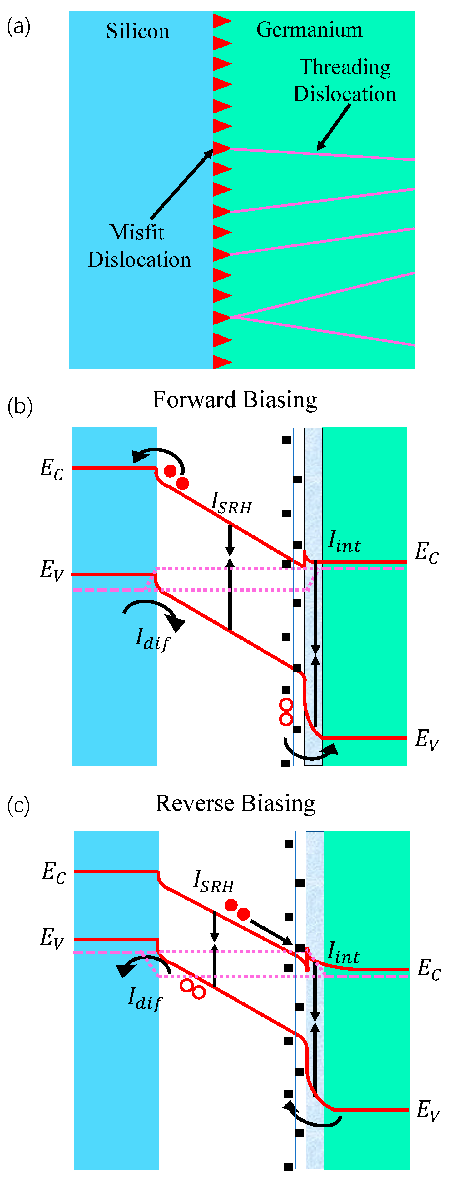
3. Physical Mechanisms
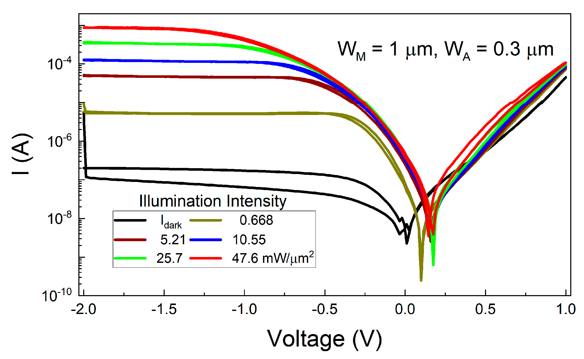
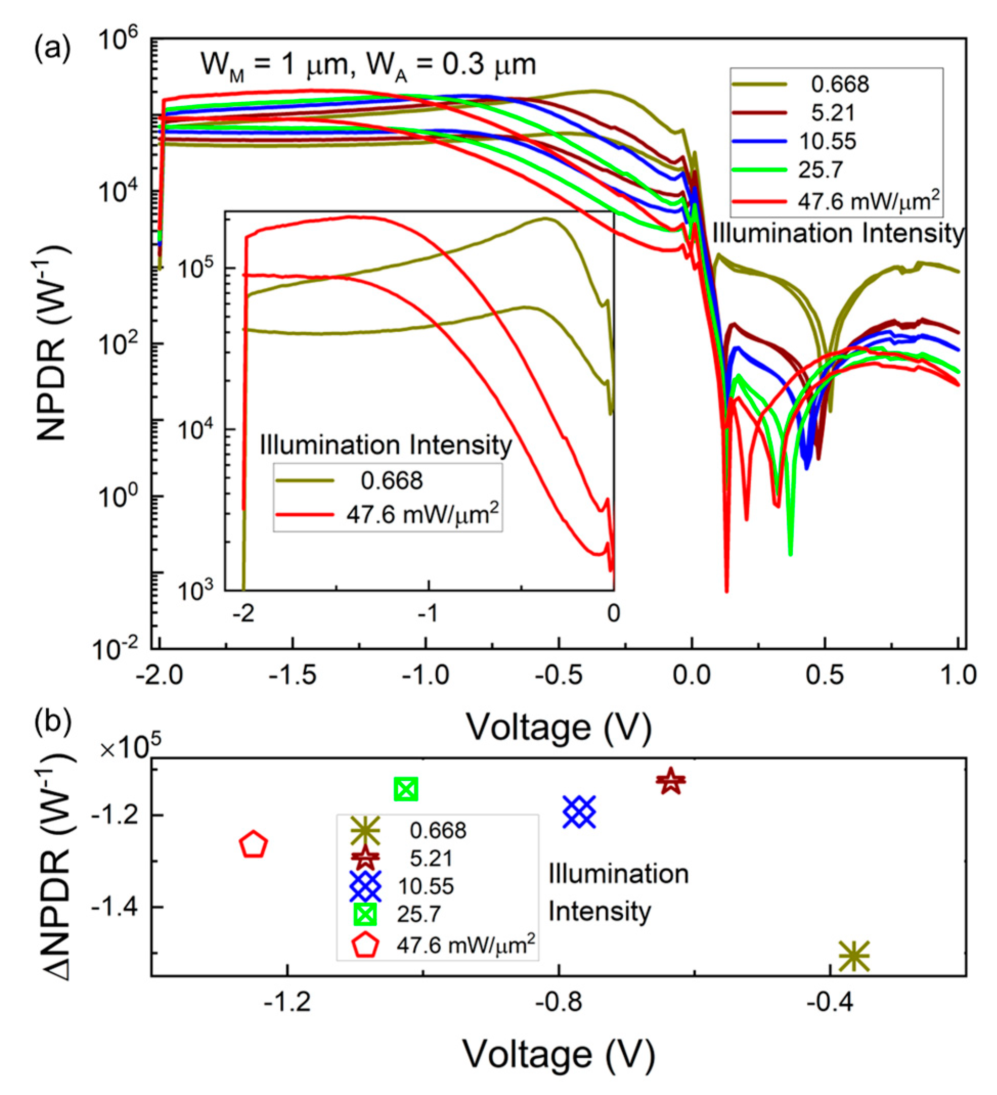
4. Results and Discussion
5. Conclusions
Author Contributions
Funding
Data Availability Statement
Conflicts of Interest
References
- Fleming, F.; Yi, X.; Mirza, M.M.A.; Jin, X.; Kirdoda, J.; Dumas, D.C.S.; Saalbach, L.; Modak, M.; Muir, D.A.S.; Smith, C.; et al. Surface-normal illuminated pseudo-planar Ge-on-Si avalanche photodiodes with high gain and low noise. Opt. Express 2024, 32, 19449–19457. [Google Scholar] [CrossRef]
- Yuan, Y.; Tossoun, B.; Huang, Z.; Zeng, X.; Kurczveil, G.; Fiorentino, M.; Liang, D.; Beausoleil, R.G. Avalanche photodiodes on silicon photonics. J. Semicond. 2022, 43, 021301. [Google Scholar] [CrossRef]
- Liu, X.; Li, X.; Li, Y.; Li, Y.; Zhi, Z.; Tao, M.; Chen, B.; Zhang, L.; Guo, P.; Lo, G.; et al. Three-terminal germanium-on-silicon avalanche photodiode with extended p-charge layer for dark current reduction. Photonics Res. 2022, 10, 1956. [Google Scholar] [CrossRef]
- Li, Y.; Liu, X.; Li, X.; Wang, S.; Ye, H.; Zhang, L.; Li, Y.; Sun, S.; Chen, B.; Ma, Y.; et al. Surface illuminated interdigitated Ge-on-Si photodetector with high responsivity. Opt. Express 2021, 29, 16346–16361. [Google Scholar] [CrossRef]
- Yi, X.; Greener, Z.; Fleming, F.; Kirdoda, J.; Dumas, D.C.S.; Saalbach, L.; Muir, D.A.S.; Ferre-Llin, L.; Millar, R.W.; Paul, D.J.; et al. After pulsing in Ge-on-Si single-photon avalanche diodes. IEEE Photonics Technol. Lett. 2023, 35, 959–962. [Google Scholar] [CrossRef]
- Jang, K.-S.; Kim, S.; Kim, I.G.; Oh, J.H.; Kim, S.A.; Joo, J.; Kim, G. High performance Ge-on-Si avalanche photodetector. In Proceedings of the Optical Interconnects XVI, San Francisco, CA, USA, 13–18 February 2016; Volume 9753, pp. 227–232. [Google Scholar]
- Kang, Y.; Liu, H.-D.; Morse, M.; Paniccia, M.J.; Zadka, M.; Litski, S.; Sarid, G.; Pauchard, A.; Kuo, Y.-H.; Chen, H.-W.; et al. Monolithic germanium/silicon avalanche photodiodes with 340 GHz gain–bandwidth product. Nat. Photonics 2009, 3, 59–63. [Google Scholar] [CrossRef]
- Li, Y.; Liu, X.; Li, X.; Zhang, L.; Chen, B.; Zhi, Z.; Li, X.; Zhang, G.; Ye, P.; Huang, G.; et al. Germanium-on-silicon avalanche photodiode for 1550 nm weak light signal detection at room temperature. Chinese Opt. Lett. 2022, 20, 062501. [Google Scholar] [CrossRef]
- Shi, B.; Qi, F.; Cai, P.; Chen, X.; He, Z.; Duan, Y.; Hou, G.; Su, T.; Li, S.; Chen, W.; et al. 106 Gb/s normal-incidence Ge/Si avalanche photodiode with high sensitivity. In Proceedings of the 2020 Optical Fiber Communications Conference and Exhibition (OFC), San Diego, CA, USA, 8–12 March 2020; pp. 1–3. [Google Scholar]
- Royo, S.; Ballesta-Garcia, M. An overview of LiDAR imaging systems for autonomous vehicles. Appl. Sci. 2019, 9, 4093. [Google Scholar] [CrossRef]
- Hadfield, R.H.; Leach, J.; Fleming, F.; Paul, D.J.; Tan, C.H.; Ng, J.S.; Henderson, R.K.; Buller, G.S. Single-photon detection for long-range imaging and sensing. Optica 2023, 10, 1124–1141. [Google Scholar] [CrossRef]
- Wallace, A.M.; Halimi, A.; Buller, G.S. Full waveform LiDAR for adverse weather conditions. IEEE Trans. Veh. Technol. 2020, 69, 7064–7077. [Google Scholar] [CrossRef]
- Srinivasan, S.A.; Lambrecht, J.; Guermandi, D.; Lardenois, S.; Berciano, M.; Absil, P.; Bauwelinck, J.; Yin, X.; Pantouvaki, M.; Campenhout, J.V. 56 Gb/s NRZ O-band hybrid BiCMOS-silicon photonics receiver using Ge/Si avalanche photodiode. J. Lightwave Technol. 2021, 39, 1409–1415. [Google Scholar] [CrossRef]
- Yuan, Y.; Huang, Z.; Zeng, X.; Liang, D.; Sorin, W.V.; Fiorentino, M.; Beausoleil, R.G. High responsivity Si-Ge waveguide avalanche photodiodes enhanced by loop reflector. IEEE J. Sel. Top. Quant. 2022, 28, 1–8. [Google Scholar] [CrossRef]
- Osten, H.J. Modification of growth modes in lattice-mismatched epitaxial systems: Si/Ge. Phys. Status Solidi A 1994, 145, 235–245. [Google Scholar] [CrossRef]
- Roland, C.; Gilmer, G.H. Growth of germanium films on Si(001) substrates. Phys. Rev. B 1993, 47, 16286–16298. [Google Scholar] [CrossRef]
- Lee, K.H.; Bao, S.; Wang, B.; Wang, C.; Yoon, S.F.; Michel, J.; Fitzgerald, E.A.; Tan, C.S. Reduction of threading dislocation density in Ge/Si using a heavily As-doped Ge seed layer. AIP Adv. 2016, 6, 025028. [Google Scholar] [CrossRef]
- Ye, H.; Yu, J. Germanium epitaxy on silicon. Sci. Technol. Adv. Mater. 2014, 15, 024601. [Google Scholar] [CrossRef]
- Endres, J.; Daniš, S.; Bauer, G. The misfit dislocation density profile in graded SiGe/Si(001) layers prepared at different temperatures. J. Phys. Condens. Matter. 2013, 25, 175802. [Google Scholar] [CrossRef]
- Langdo, T.A.; Leitz, C.W.; Currie, M.T.; Fitzgerald, E.A.; Lochtefeld, A.; Antoniadis, D.A. High quality Ge on Si by epitaxial necking. Appl. Phys. Lett. 2000, 76, 3700–3702. [Google Scholar] [CrossRef]
- Klinger, S.; Berroth, M.; Kaschel, M.; Oehme, M.; Kasper, E. Ge-on-Si p-i-n photodiodes with a 3-dB bandwidth of 49 GHz. IEEE Photonics Technol. Lett. 2009, 21, 920–922. [Google Scholar] [CrossRef]
- Yi, L.; Liu, D.; Li, D.; Zhang, P.; Tang, B.; Li, B.; Wang, W.; Yang, Y.; Li, Z. Waveguide-integrated Ge/Si avalanche photodiode with vertical multiplication region for 1310 nm detection. Photonics 2023, 10, 750. [Google Scholar] [CrossRef]
- Hong, C.; Shi, B.; Qi, F.; Cai, P.; Duan, Y.; Hou, G.; Su, T.; Chiu, T.; Li, S.; Chen, W.; et al. High speed Ge/Si avalanche photodiode with high sensitivity for 50Gbit/s and 100Gbit/s optical access systems. In Proceedings of the 2022 Optical Fiber Communications Conference and Exhibition (OFC), San Diego, CA, USA, 6–10 March 2022; pp. 1–3. [Google Scholar]
- Li, Y.; Liu, X.; Li, X.; Zhang, L.; Li, Y.; Chen, B.; Zhi, Z.; Gao, F.; Li, X.; Guo, P.; et al. Lateral separate absorption charge multiplication Ge-on-Si avalanche photodiode with low dark current in linear mode. Opt. Commun. 2022, 518, 128343. [Google Scholar] [CrossRef]
- Deeb, H.; Khomyakova, K.; Kokhanenko, A.; Douhan, R.; Lozovoy, K. Dependence of Ge/Si avalanche photodiode performance on the thickness and doping concentration of the multiplication and absorption layers. Inorganics 2023, 11, 303. [Google Scholar] [CrossRef]
- Song, J.; Bin, S.; Zhou, C.; Qin, B. High-performance normal-incidence Ge/Si meta-structure avalanche photodetector. Photonics 2023, 10, 780. [Google Scholar] [CrossRef]
- Chen, H.; Verheyen, P.; De Heyn, P.; Lepage, G.; De Coster, J.; Balakrishnan, S.; Absil, P.; Yao, W.; Shen, L.; Roelkens, G.; et al. −1 V bias 67 GHz bandwidth Si-contacted germanium waveguide p-i-n photodetector for optical links at 56 Gbps and beyond. Opt. Express 2016, 24, 4622–4631. [Google Scholar] [CrossRef]
- Zhang, D.; Xue, C.; Cheng, B.; Su, S.; Liu, Z.; Zhang, X.; Zhang, G.; Li, C.; Wang, Q. High-responsivity GeSn short-wave infrared p-i-n photodetectors. Appl. Phys. Lett. 2013, 102, 141111. [Google Scholar] [CrossRef]
- Shim, J.; Kang, D.H.; Yoo, G.; Hong, S.T.; Jung, W.S.; Kuh, B.J.; Lee, B.; Shin, D.; Ha, K.; Kim, G.S.; et al. Germanium p-i-n avalanche photodetector fabricated by point defect healing process. Opt. Lett. 2014, 39, 4204–4207. [Google Scholar] [CrossRef]
- Kim, I.G.; Jang, K.-S.; Joo, J.; Kim, S.; Kim, S.; Choi, K.-S.; Oh, J.H.; Kim, S.A.; Kim, G. High-performance photoreceivers based on vertical-illumination type Ge-on-Si photodetectors operating up to 43 Gb/s at λ~1550nm. Opt. Express 2013, 21, 30716–30723. [Google Scholar] [CrossRef]
- Alam, M.S.; Rahman, M.S.; Islam, M.R.; Bhuiyan, A.G.; Yamada, M. Refractive index, absorption coefficient, and photoelastic constant: Key parameters of ingaas material relevant to ingaas-based device performance. In Proceedings of the 2007 IEEE 19th International Conference on Indium Phosphide & Related Materials, Matsue, Japan, 14–18 May 2007; pp. 343–346. [Google Scholar]
- Li, C.; Xue, C.; Li, C.; Liu, Z.; Cheng, B.; Wang, Q. High bandwidth surface-illuminated InGaAs/InP uni-travelling-carrier photodetector. Chin. Phys. B 2013, 22, 118503. [Google Scholar] [CrossRef]
- Li, C.; Li, B.; Qin, S.; Su, J.; He, X.; Guo, X. Effects of interface states on Ge-On-SOI photodiodes. IEEE J. Electron Devices Soc. 2019, 7, 7–12. [Google Scholar] [CrossRef]
- Gity, F.; Hayes, J.M.; Corbett, B.; Morrison, A.P. Modeling the effects of interface traps on the static and dynamic characteristics of Ge/Si avalanche photodiodes. IEEE J. Quantum Electron. 2011, 47, 849–857. [Google Scholar] [CrossRef]
- DeRose, C.T.; Trotter, D.C.; Zortman, W.A.; Starbuck, A.L.; Fisher, M.; Watts, M.R.; Davids, P.S. Ultra compact 45 GHz CMOS compatible Germanium waveguide photodiode with low dark current. Opt. Express 2011, 19, 24897–24904. [Google Scholar] [CrossRef]
- Eaglesham, D.J.; Cerullo, M. Dislocation-free Stranski-Krastanow growth of Ge on Si(100). Phys. Rev. Lett. 1990, 64, 1943–1946. [Google Scholar] [CrossRef]
- LeGoues, F.K.; Copel, M.; Tromp, R.M. Microstructure and strain relief of Ge films grown layer by layer on Si(001). Phys. Rev. B 1990, 42, 11690–11700. [Google Scholar] [CrossRef]
- Forrest, S.R.; Leheny, R.F.; Nahory, R.E.; Pollack, M.A. In0.53Ga0.47As photodiodes with dark current limited by generation-recombination and tunneling. Appl. Phys. Lett. 1980, 37, 322–325. [Google Scholar] [CrossRef]
- Chen, Z.; Jie, B.B.; Sah, C.-T. Effects of energy distribution of interface traps on recombination dc current-voltage line shape. J. Appl. Phys. 2006, 100, 114511. [Google Scholar] [CrossRef]
- Miyasaka, Y.; Hiraki, T.; Okazaki, K.; Takeda, K.; Tsuchizawa, T.; Yamada, K.; Wada, K.; Ishikawa, Y. Ge/graded-SiGe multiplication layers for low-voltage and low-noise Ge avalanche photodiodes on Si. Jpn. J. Appl. Phys. 2016, 55, 04EH10. [Google Scholar] [CrossRef]
- Hsin, C.-L.; Chou, C.-H. Buffer-free Ge/Si by rapid melting growth technique for separate absorption and multiplication avalanche photodetectors. IEEE Electron Device Lett. 2019, 40, 945–948. [Google Scholar] [CrossRef]
- Wanitzek, M.; Schulze, J.; Oehme, M. Ge-on-Si single-photon avalanche diode using a double mesa structure. Opt. Lett. 2024, 49, 6345–6348. [Google Scholar] [CrossRef]
- Lee, K.; Jandl, A.; Tan, Y.; Fitzgerald, E.; Tan, C. Growth and characterization of germanium epitaxial film on silicon (001) with germane precursor in metal organic chemical vapour deposition (MOCVD) chamber. AIP Adv. 2013, 3, 092123. [Google Scholar] [CrossRef]
- Lee, K.H.; Tan, Y.H.; Jandl, A.; Fitzgerald, E.A.; Tan, C.S. Comparative studies of the growth and characterization of germanium epitaxial film on silicon (001) with 0° and 6° offcut. J. Electron. Mater. 2013, 42, 1133–1139. [Google Scholar] [CrossRef]
- Michel, J.; Camacho-Aguilera, R.E.; Cai, Y.; Patel, N.; Bessette, J.T.; Romagnoli, M.; Dutt, B.; Kimerling, L.C. An Electrically pumped Ge-on-Si laser. In Proceedings of the OFC/NFOEC, Angeles, CA, USA, 4–8 March 2012; pp. 1–3. [Google Scholar]
- Marković, L.; Knežević, T.; Nanver, L.K.; Attariabad, A.; Azizur-Rahman, K.M.; Mah, J.J.; Wang, K.L.; Suligoj, T. Impact of the Ge-Si interfacial barrier on the temperature-dependent performance of pureGaB Ge-on-Si p + n photodiodes. Opt. Express 2024, 32, 35542–35550. [Google Scholar] [CrossRef]
- Pan, R.; Yuan, Z.; Zhang, K.; Yao, J.; Li, C.; Lu, M.; Lu, H.; Chen, Y.-F. Annealing induced carrier activation and PL enhancement in Ge-on-Si grown by low temperature MBE. J. Cryst. Growth 2022, 588, 126668. [Google Scholar] [CrossRef]
- Wei, Y.; Cai, X.; Ran, J.; Yang, J. Analysis of dark current dependent upon threading dislocations in Ge/Si heterojunction photodetectors. Microelectron. Int. 2012, 29, 136–140. [Google Scholar] [CrossRef]
- Huang, Z.; Oh, J.; Banerjee, S.K.; Campbell, J.C. Effectiveness of SiGe buffer layers in reducing dark currents of Ge-on-Si photodetectors. IEEE J. Quantum Electron. 2007, 43, 238–242. [Google Scholar] [CrossRef]
Disclaimer/Publisher’s Note: The statements, opinions and data contained in all publications are solely those of the individual author(s) and contributor(s) and not of MDPI and/or the editor(s). MDPI and/or the editor(s) disclaim responsibility for any injury to people or property resulting from any ideas, methods, instructions or products referred to in the content. |
© 2025 by the authors. Licensee MDPI, Basel, Switzerland. This article is an open access article distributed under the terms and conditions of the Creative Commons Attribution (CC BY) license (https://creativecommons.org/licenses/by/4.0/).
Share and Cite
Zhao, D.; Shao, Y.; Zhang, S.; Li, T.; Chi, B.; Zhu, Y.; Liu, F.; Liang, Y.; Du, S. Impact of Charge Carrier Trapping at the Ge/Si Interface on Charge Transport in Ge-on-Si Photodetectors. Electronics 2025, 14, 2982. https://doi.org/10.3390/electronics14152982
Zhao D, Shao Y, Zhang S, Li T, Chi B, Zhu Y, Liu F, Liang Y, Du S. Impact of Charge Carrier Trapping at the Ge/Si Interface on Charge Transport in Ge-on-Si Photodetectors. Electronics. 2025; 14(15):2982. https://doi.org/10.3390/electronics14152982
Chicago/Turabian StyleZhao, Dongyan, Yali Shao, Shuo Zhang, Tanyi Li, Boming Chi, Yaxing Zhu, Fang Liu, Yingzong Liang, and Sichao Du. 2025. "Impact of Charge Carrier Trapping at the Ge/Si Interface on Charge Transport in Ge-on-Si Photodetectors" Electronics 14, no. 15: 2982. https://doi.org/10.3390/electronics14152982
APA StyleZhao, D., Shao, Y., Zhang, S., Li, T., Chi, B., Zhu, Y., Liu, F., Liang, Y., & Du, S. (2025). Impact of Charge Carrier Trapping at the Ge/Si Interface on Charge Transport in Ge-on-Si Photodetectors. Electronics, 14(15), 2982. https://doi.org/10.3390/electronics14152982