Abstract
Electromagnetic interference (EMI) has become a significant issue as electronic devices become more integrated and achieve high performance. In order to operate at high performance in an integrated system, a high-frequency clock signal is essential to enhance processing speed. However, the harmonic component of the clock signal or gate signal is one of the major EMI sources that can cause peripheral devices to malfunction and affect their stability and reliability. In this paper, harmonic component analysis of the MOSFET gate signal which depends on gate resistance is conducted. Based on theoretical analysis using Fourier series expansion, gate resistance contributes to harmonic components that are determined by the rising and falling times of a gate signal. Simulation and measurement are conducted using a buck converter as a practical application. The theoretical analysis is validated by simulation and experimental results demonstrate that the magnitude of the harmonics is reduced because increasing the gate resistance extends the rising and falling times.
1. Introduction
Recently, electronic devices have been increasingly integrated and designed for enhanced performance. For example, the rated power, number of transistors, and clock frequency of microprocessors which are widely used in electronic devices have been gradually increasing [,]. Specifically, high-frequency clock signals, one of the major electromagnetic interference (EMI) sources, cause EMI problems in peripheral devices.
Typically, EMI can affect communication between the transmitter and receiver, resulting in a malfunction of devices. For a practical case of an EMI effect in communication, ambient noise in the image around unshielded magnetic resonance imaging (MRI) was investigated, where the noise components generated by external EMI coils interfere with the receiver coil of the MRI, leading to distorted images [,].
In practical power electronics applications, EMI is a critical concern due to the frequent variations in voltage and current caused by switching operations and relatively high-power operating conditions. Controlling EMI is essential in power electronics. For this reason, many studies have been conducted to reduce the EMI generated by power conversion systems. For example, studies have been conducted not only on EMI reduction in wireless charging electric vehicles [,], but also on the effects of EMI and corresponding mitigation strategies in unmanned aerial vehicles [,].
Common approaches include the use of additional filters in power conversion circuits [,] and spread spectrum techniques, which employ variable clock frequency signals to drive switches [,,,,,]. In particular, since the switching device itself is a major source of noise, research has focused on analyzing the noise generated by switching operations and on developing gate drivers to suppress such noise [,,,,]. Additionally, some research groups have focused on optimizing the power delivery network (PDN). However, effective EMI control often requires careful consideration during the initial PCB layout and component selection stages [,]. Post-layout strategies, such as implementing shielding or increasing the spatial separation from noise sources, are generally less effective and tend to increase design complexity and cost. As a result, due to the complexity and relatively high cost of these conventional methods, it is essential to explore simplified analysis techniques and design approaches for EMI reduction.
One solution is to control the switching transition time. Although increasing the transition time of the MOSFET introduces additional switching losses, adjusting the transition time can enhance system robustness and reduce harmonic noise that may affect nearby systems. Therefore, since the transition time can be determined by the circuit model, theoretical analysis of the transition model of the MOSFET is significant for power electronics modules.
In this study, a practical technique to reduce EMI by modifying a single resistor value within an existing circuit topology is analyzed. The switching noise at the MOSFET gate is theoretically evaluated, and harmonic reduction by controlling the gate resistance is proposed. Theoretical analysis confirms that gate resistance (RG) and the parasitic capacitances of the MOSFET are the primary parameters influencing the magnitude of harmonic components. This analysis can contribute to reducing radiated emissions with minimal impact on overall system design, providing a low-cost and compact solution for EMI control. Because the parasitic parameters are practically uncontrollable due to their physical structure and manufacturing process [], this research mainly focuses on the effects of gate resistance. For this reason, the analysis is conducted at the MOSFET device level, considering parasitic capacitances and gate resistance which affect the turn-on and turn-off behavior of the MOSFET. In addition, to confirm the tendency of switching noise in practical applications, the switch in the power conversion system is designed. In order to validate in power conversion system, a low-side DC-DC buck converter is selected, as the low-side buck converter is widely used due to the advantages of the low-side topology explained in [,,].
2. Theoretical Modeling Based on MOSFET Device
In order to investigate the effect of RG on the harmonic components, switching noise modeling is performed under the device level of the MOSFET and a no-load condition to decrease the complexity of the analysis. In this work, the definitions of the symbols are listed in Table 1.

Table 1.
Definition of Symbols.
An equivalent circuit for theoretical modeling is illustrated in Figure 1a. As illustrated, the drain of the MOSFET is shorted to ground to represent the no-load condition.
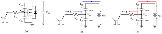
Figure 1.
Equivalent circuit of a MOSFET for theoretical modeling: (a) MOSFET model including gate resistance and parasitic capacitance under a no-load condition; (b) parasitic capacitance (CGS) charging stage model representing the turn-on state, (c) parasitic capacitance discharging stage model representing the turn-off state.
Here, the parasitic capacitance between the gate and source terminals, and the parasitic capacitance between the gate and drain terminals are denoted as CGS and CGD, respectively. In order to assume the operating condition of the MOSFET, a driving circuit consisting of VG, RG, and VDS which represent the gate signal high level, gate resistance, and drain-source voltage, respectively, is considered. Also, in this research, the switching noise is focused on gate-source voltage (VGS) that determines turn-on and -off states of the MOSFET. The turn-on and -off states are represented in Figure 1b and Figure 1c, respectively, with a modified equivalent circuit for simplicity. Specifically, Figure 1b shows that the IG, driven by the VG, is divided into IGS and IGD. When CGS is charged by the current IGS, the VGS increases above the threshold voltage of the MOSFET (Vth), and the MOSFET turns on. On the other hand, as illustrated in Figure 1c, when the VG becomes zero, the charge stored in CGS and CGD introduces IGS and IGD, discharging both capacitors. As a result, when the VGS drops below Vth, the MOSFET turns off.
2.1. Transient Response of Gate-Source Voltage
To evaluate switching noise, Kirchhoff’s current law (KCL) is applied to the VGS node. Additionally, the duration of the turn-on and -off states is assumed to be equal. Equation (1) represents the relationship between input and output currents at the VGS node, and can be expressed in terms of the node voltages.
Each current term can be represented as stated in the following equations.
Assuming a constant VDS, as the differential of VDS becomes zero, IGD(t) can be modified as in Equation (5).
By utilizing Equations (2), (3) and (5), Equation (1) can be written as
The turn-on transient response can be obtained by solving the differential equation in Equation (6), which is given as
By using Equation (7), the transient response of the MOSFET turn-on state can be obtained.
In the case of a turn-off state, as VG is zero, the CGS and CGD begin to discharge, resulting in the VGS becoming zero.
Due to the discharge of the parasitic capacitances during the turn-off state with a constant VDS, Equation (9) is rewritten as
By applying a similar procedure to that in Equation (6) to the turn-off state, the following equation is derived as
As a result, the turn-off transient response is formulated as
Here, VG in the turn-on state is substituted by VGS,on,max since the turn-off state follows the turn-on state.
Based on Equations (7) and (12), it is revealed that transient responses are dominantly determined by RG, CGS, and CGD. This means that appropriate values for RG, CGS, and CGD are significant for operating the MOSFET under desirable transient conditions. However, considering that the parasitic capacitances (CGS, CGD) are difficult to control due to their dependence on the physical structure, the effect of RG, which is more conveniently controllable, is analyzed.
In order to verify the theoretical analysis, circuit simulation results obtained by using OrCAD PSpice are compared with the transient responses. The simulation conditions correspond to Figure 1a, and the circuit parameters are listed in Table 2.
Table 2.
Circuit parameters of equivalent circuits.
Because of uncontrollable parasitic elements, the comparison results for the variation in RG are presented in Figure 2.
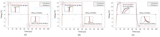
Figure 2.
Calculation and simulation results of transient response under no-load condition: (a) RG = 1 Ω; (b) RG = 100 Ω; (c) RG = 1 kΩ.
To clearly observe the effect of RG, the values of RG were chosen as 1 Ω, 100 Ω, and 1 kΩ, corresponding to cases 1, 2, and 3, respectively. As shown in Figure 2a–c, the rising time and falling time increase as RG increases. Also, the similarity in the slope, which is depicted near the points of full turn-on and turn-off, supports Equations (7) and (12).
2.2. Frequency Component Calcaulted by Fourier Coefficient
Based on Equations (7) and (12), it is essential to identify the frequency components using Fourier series expansion derived as Equation (13). The magnitude of the frequency components in the transient responses is determined by the cn which is calculated through an and bn, as expressed in Equations (14)–(16). The a0 represents the average of the transient response, while an and bn are defined as the Fourier coefficients of the cosine and sine terms, respectively, with a period of T and a harmonic order of n. Here, the coefficients an and bn are given by Equations (17) and (18) in terms of circuit parameters, with the gate signal high level VG and rising and falling times (τ) defined in Equation (19). The theoretical analysis of harmonic components is demonstrated by the Fast Fourier Transform (FFT) result of the transient responses.
The comparison was conducted under the same condition as the transient response with respect to RG, and frequency components are depicted from the fundamental frequency (10 kHz) up to the 11th harmonic. The comparison results between the calculated frequency components using Fourier coefficients and the FFT of the transient simulation are illustrated in Figure 3.
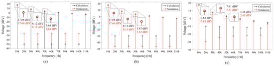
Figure 3.
Calculation and simulation results of frequency component under no-load condition: (a) RG = 1 Ω; (b) RG = 100 Ω; (c) RG = 1 kΩ.
As shown in Figure 3a–c, frequency components decrease as RG increases and similarity between theoretical analysis and simulation results are observed. These results support that the Fourier coefficients are dominant in τ and that variations in τ determine harmonic components, as given in Equations (17) and (18). When focusing on the odd harmonic components, the calculation and simulation results correspond for RG = 1 Ω and RG = 100 Ω. However, for RG = 1 kΩ, an error rate of less than 16% is observed. The error comes from the differences between the circuit model and the SPICE model, which incorporates a dynamic capacitance model. Specifically, the Miller plateau can be observed in the SPICE model, whereas it is not considered in the circuit model to reduce complexity [].
2.3. Determination of RG Considering Switching Loss
Though the increasing RG reduces EMI-related harmonic components, which are generated by the harmonic components of VGS which are mathematically derived and confirmed by simulation, it also leads to increased switching losses (PLoss), which can be calculated as the integral of the product of the drain-source voltage and the channel current (ich) during the switching process, and are proportional to the switching frequency (fsw), as described in Equation (20) [,].
In this research, regarding the transition time, the rising/falling time is denoted as τ, which is the product of RG and CGS + CGD, and RG is directly proportional to τ and, consequently, to the rising time. In practice, determining an exact RG value is challenging because the parasitic capacitance of MOSFETs varies depending on the manufacturer. Therefore, it is advisable to refer to the datasheets given by manufacturers, which typically include experimental data. Although the optimal RG value may vary depending on the characteristics of the MOSFET, it is generally selected to be below a few hundred ohms [,,,]. The focus of this research is the theoretical evaluation and observation of the harmonic reduction trend depending on different RG values, ranging from 1 Ω to 1 kΩ in simulation and from 1 Ω to 300 Ω in experimentation.
3. Low-Side Buck Converter with RG Control
In order to demonstrate the proposed idea, a buck converter is considered. In general, a buck converter composed of an auxiliary circuit such as a bootstrap, charge pump, or pulse transformer is necessary because the source voltage of the N-type MOSFET is floating from the ground. In this research, not only to avoid additional components but also to observe switching noise in VGS with respect to the ground, the low-side buck converter topology is employed which utilizes an N-type MOSFET on the low side.
3.1. Configuration of the Low-Side Buck Converter
A circuit diagram for simulation is shown in Figure 4, and the IRF530N (Infineon) is selected for the MOSFET.
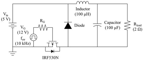
Figure 4.
The low-side buck converter used for simulation. Ideal inductor, capacitor, and diode components from the PSpice library were utilized.
In order to consider practical characteristics, the internal SPICE model in PSpice is used for the IRF530N, with CGS and CGD corresponding to 0.89 nF and 0.45 nF, respectively. For the gate signal, a pulse voltage source with a trapezoidal waveform due to its rising and falling time was used. Regarding the capacitor, inductor and diode, ideal components from the PSpice library were utilized. The DC input voltage is restricted to 5 V to emphasize the effect of switching noise caused by VGS. The gate resistance is set to 1 Ω, 100 Ω, and 1 kΩ, similar to the previous simulation at the device level of switch, and the detailed circuit parameters are shown in Figure 4. Additionally, simulations were conducted using a transient solver in the PSpice and the maximum time step was set to 10 ns to enable fine time resolution during the rising and falling transitions of the VGS. In this case, the VGS is monitored at the observation point using a voltage probe and the frequency components are extracted through the FFT function in the simulation.
3.2. Simulation Results
The observed transient responses of VGS in the low-side buck converter are represented in Figure 5.
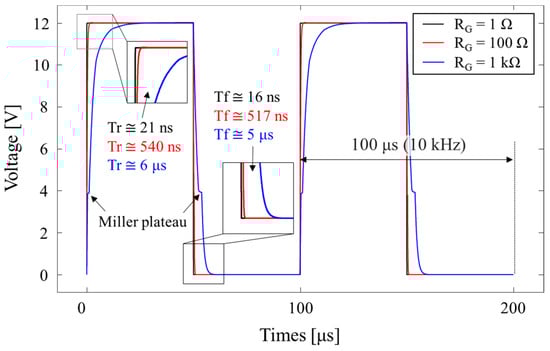
Figure 5.
Transient response of low-side buck converter for simulation.
Consistent with results at the device level, the rising and falling times of VGS increase as RG increases, whereas they decrease as RG decreases. In the case of an RG equal to 1 kΩ, the VGS remains at approximately 4 V for a certain duration, which is known as a Miller plateau []. This Miller plateau also extends both the rising and falling times.
In Figure 6, frequency components are confirmed from 10 kHz up to 300 kHz to investigate the effect of switching noise in a power conversion system.
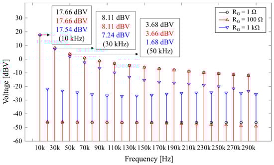
Figure 6.
FFT result of low-side buck converter for simulation.
Here, the dBV unit was utilized to facilitate the observation of fine frequency components. Although frequency components are irregular with an RG value of 1 kΩ due to the Miller plateau, the magnitudes of harmonics follow a consistent trend that is similar to the device-level results. From the results, the magnitudes of the high-frequency harmonics were reduced, except for the even-order components, which are relatively negligible.
4. Experimental Validation
In order to verify harmonic reduction by increasing RG, experiments with various RG values were conducted. The switching noise in VGS is measured under similar conditions as the simulation in a low-side buck converter.
4.1. Fabricated Low-Side Buck Converter and Measurement Setup
The fabricated low-side buck converter for measurement was built on a perfboard as shown in Figure 7.
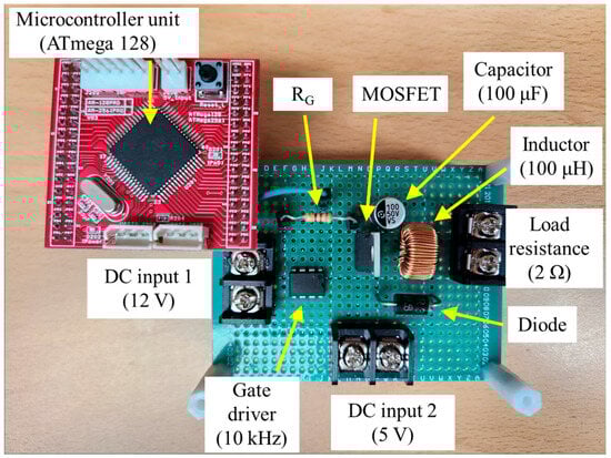
Figure 7.
Fabricated low-side buck converter for transient response and frequency component measurements.
The ATmega128 module, used as the microcontroller unit (MCU), is placed in the upper left corner to provide the gate signal through the RG and the gate driver. For the gate driver, the IR2184 (Infineon) is used to boost a 5 V pulse to 12 V and is supplied by DC input 1. As in the simulation, the IRF530N is used as the MOSFET with its parasitic capacitance varying depending on the drain-source voltage and being given as a range in the datasheet, unlike the theoretical and simulation results []. Thus, the measured value of CGS is in the range of 0.86–0.90 nF and CGD is in the range of 0.30–0.45 nF. The DC input 2 and load resistance are connected to the DC input and the electronic load of the low-side buck converter, respectively.
The experimental setup is illustrated in Figure 8, consisting of power supplies, an oscilloscope (Keysight DSOX4024A) for waveform monitoring, measurement probes including a passive probe (Keysight N2894A), a differential probe (Keysight N2791A), and current probes (Keysight N2782B), and an electronic load (Kikusui PLZ1205W) functioning as a load resistor.
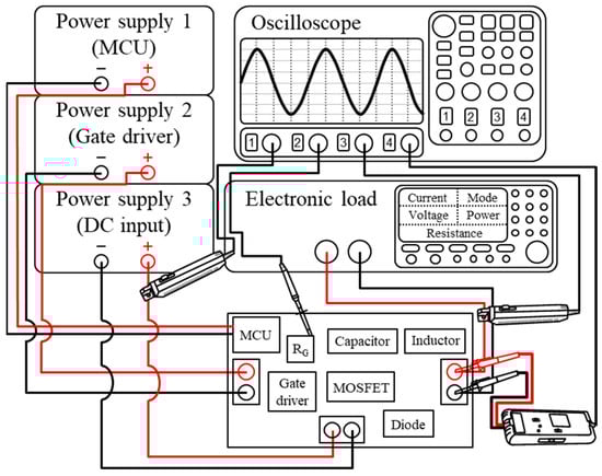
Figure 8.
Measurement setup for transient response and frequency components.
The DC output voltage is measured using the differential probe, while the DC input current and DC output current are measured using the current probes. In addition, the transient response of VGS is measured by the passive probe, and frequency components are extracted through the internal FFT function in the oscilloscope. The load resistance is set to 2 Ω via the constant resistance function in the electronic load, and the rest of the detailed experimental parameters are represented in Figure 7. In order to ensure stable power delivery and minimize interference, three power supplies are employed in the experiment. The ATmega128, IR2184, and the DC input of the low-side buck converter are powered by power supplies 1, 2, and 3, respectively. Since a 1 kΩ gate resistance is rarely used for practical applications, the measurement is conducted with RG values of 1 Ω, 10 Ω, and 300 Ω.
4.2. Expermental Results
The experimental results are also compared with the simulation results for various RG. Figure 9 shows the measured VGS on an oscilloscope. Since the MCU is designed to generate a 10 kHz switching frequency, it is observed consistently in all cases. Also, as discussed in Section 2 with Equation (19), as the RG increases, the rising time and falling time increases. This phenomenon is also verified in the simulated results. Specifically, when the RG varies from 1 Ω, to 10 Ω, to 300 Ω, the measured rising time changes from 18ns, to 71 ns, to 1.5 µs, respectively. The measured falling time is 17 ns, 74, ns and 1 µs as the RG increases. These results correspond with the simulation results, which is attributed to the use of an identical component spice model.
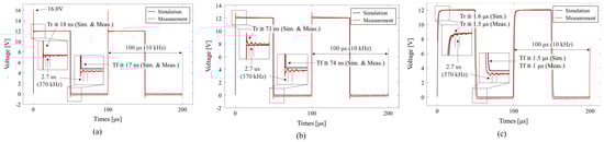
Figure 9.
Transient response of low-side buck converter for measurement and simulation: (a) RG = 1 Ω; (b) RG = 10 Ω; (c) RG = 300 Ω.
While the rising time and falling time correspond to each other, ringing is observed in the experimental results. As illustrated in Figure 9a,b, ringing is more prevalent when the RG is 1 Ω and 10 Ω compared to when the RG is 300 Ω, as shown in Figure 9c. Specifically, when RG is equal to 1 Ω, the overshoot reaches nearly 16 V, and the frequency of the ringing is approximately 370 kHz. These phenomena are due to the unexpected internal parasitic components in the fabricated low-side buck converter. Practically, a resistance that is used for a gate resistance also includes parasitic inductance and capacitance. Also, the input and output terminals have parasitic capacitance in practice, and even solder joints and wires connecting the electronic components introduce parasitic inductance. These parasitic components are inevitably present when fabricating the buck converter. However, the parasitic components on the board are beyond the scope of this research, as the focus was to confirm the reduction of harmonic components by varying the gate resistance. Thus, except for the effect of parasitic components, the relationship between the rising and falling times and switching noise in practical applications is validated.
Figure 10 represents the comparison of the magnitudes of frequency components, from fundamental frequency (10 kHz) up to the 11th harmonic (110 kHz). As expected from previous results, the magnitude of frequency components decreases as RG increases, which follows the consistent trend. Specifically, the 5th harmonic decreased by approximately 0.2 dB at most, while the fundamental frequency component remained nearly constant despite the increase in RG. The measurement and simulation errors in fundamental and harmonic components are due to the gate driver, IRS2184, which is designed to provide low-side and high-side gate signals simultaneously and includes an internal 500 ns dead time to prevent shoot-through []. The internal dead time leads to errors in the duty cycle of the pulse signal, which causes the duty to be slightly lower or higher than 50%, resulting in errors in odd and even harmonic components. For this reason, except for the effect of the gate driver, the switching noise in power conversion systems can be reduced by selecting an appropriate RG.
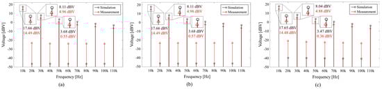
Figure 10.
FFT result of low-side buck converter for measurement and simulation: (a) RG = 1 Ω; (b) RG = 10 Ω; (c) RG = 300 Ω.
Figure 11 illustrates the merged results from Figure 10a–c with a linear scale. In this figure, it can be noticeable that as the RG increases, the absolute value of the harmonic component decreases, thereby improving EMI performance. This supports the theoretical analysis with experimental results.
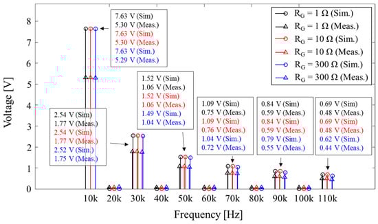
Figure 11.
Comparison of the absolute values of the harmonic component comparison result of the low-side buck converter for measurement and simulation with various RG values (linear scale).
5. Discussions
This paper covers the analytical analysis behavior of a MOSFET depending on RG. Though this research discusses only the effect of a single MOSFET, in practice, power conversion systems typically use multiple MOSFETs. The proposed RG selection and theoretical analysis contribute to reducing harmonic components, as each component’s amplitude is subject to superposition, thereby affecting the system-level harmonic distribution. The limitation of this article is that temperature and other environmental conditions are not considered. In practice, MOSFETs can exhibit different behaviors under varying temperatures and atmospheric pressures [,]. Therefore, a comprehensive analysis that accounts for temperature variations and other specific environmental conditions could be an important direction for future research to enhance the robustness and applicability of the proposed methodology.
6. Conclusions
In this paper, the control of gate-source voltage with respect to the variation of gate resistance is evaluated in order to reduce switching noise in the MOSFET.
To analyze the adjustment of the gate-source voltage, the equivalent circuit for MOSFET switching considering parasitic capacitances is used. The transient response is modeled from the equivalent circuit and the frequency components are derived by Fourier series expansion. The theoretical analysis is verified through simulations and measurements of the low-side buck converter, as well as simulations at the device level of the MOSFET. As theoretically explained, the experimental results confirm that the harmonic components in a power conversion system can be reduced by using an appropriate gate resistance. As a result, regardless of the topology, for modules that include MOSFETs, selecting an appropriate gate resistance can be an effective option to reduce harmonic EMI components.
Author Contributions
Conceptualization, J.C. and D.K.; methodology, D.K.; validation, J.C. and D.K.; formal analysis, J.C.; investigation, J.C.; data curation, J.C.; writing—original draft preparation, J.C.; writing—review and editing, D.K.; supervision, D.K.; project administration, D.K.; funding acquisition, D.K. All authors have read and agreed to the published version of the manuscript.
Funding
This work was supported by the Yeungnam University Research Grant (No. 222A580033).
Data Availability Statement
The original contributions presented in this study are included in the article. Further inquiries can be directed to the corresponding author.
Conflicts of Interest
The authors declare no conflict of interest.
References
- Radhakrishnan, K.; Swaminathan, M.; Bhattacharyya, B.K. Power delivery for high-performance microprocessors—Challenges, solutions, and future trends. IEEE Trans. Compon. Packag. Manuf. Technol. 2021, 11, 655–671. [Google Scholar] [CrossRef]
- Yao, J.; Lai, Y.; Ma, Z.; Wang, S. Investigation of noise spectrum and radiated EMI in high switching frequency flyback converters. In Proceedings of the 2021 IEEE Applied Power Electronics Conference and Exposition (APEC), Phoenix, AZ, USA, 14–17 June 2021. [Google Scholar] [CrossRef]
- Lu, R.; Wu, Z.; Zhang, G.; Hu, X.; Liu, Y.; Jiang, X.; Ni, Z.; Yi, H. Electromagnetic interference rejection strategy for 50-mT portable unshielded whole-body magnetic resonance imaging with a convolutional neural network incorporating attention mechanism. IEEE Trans. Instrum. Meas. 2025, 74, 4506408. [Google Scholar] [CrossRef]
- Huang, Y.; Qu, S.; Xie, Y.; Wang, H.; Zhang, X.L.; Zhang, X.T. Inter-channel correlation-based EMI noise removal (ICER) for shielding-free low-field MRI. IEEE Trans. Biomed. Eng. 2025; in press. [Google Scholar] [CrossRef]
- Woo, S.; Shin, Y.; Rhee, J.; Huh, S.; Ahn, S. Design of Resonant Circuit Components to Suppress both EMF and EMI in Wireless Power Transfer Systems for Electric Vehicles. IEEE J. Emerg. Sel. Top. Power Electron. 2025; in press. [Google Scholar] [CrossRef]
- Sulejmani, E.; Beltle, M.; Tenbohlen, S. EMC of Inductive Automotive Charging Systems According to Standard SAE J2954. Vehicles 2023, 5, 1532–1552. [Google Scholar] [CrossRef]
- Jie, H.; Zhao, Z.; Li, H.; Gan, T.H.; See, K.Y. A Systematic Three-Stage Safety Enhancement Approach for Motor Drive and Gimbal Systems in Unmanned Aerial Vehicles. IEEE Trans. Power Electron. 2025, 40, 9329–9342. [Google Scholar] [CrossRef]
- Rad, S.S.; Zheng, Z.; Kheirollahi, R.; Mostafa, A.; Zhao, S.; Wang, Y.; Chevinly, J.; Nadi, E.; Bensala, T.; Zhang, H.; et al. Electromagnetic Interference on Unmanned Aerial Vehicles (UAVs): A Case Study of High Power Transmission Line Impacts. IEEE Trans. Transp. Electrif. 2025, 11, 7501–7513. [Google Scholar] [CrossRef]
- Darisi, M.; Caldognetto, T.; Biadene, D.; Stellini, M. Digital active EMI filter for smart electronic power converters. Electronics 2024, 13, 3889. [Google Scholar] [CrossRef]
- Zhang, Y.; Li, H.; Shi, Y. Electromagnetic interference filter design for a 100 kW silicon carbide photovoltaic inverter without switching harmonics filter. IEEE Trans. Ind. Electron. 2022, 69, 6925–6934. [Google Scholar] [CrossRef]
- Kim, H.; Kim, J.; Jeong, S.; Lee, S.; Cho, Y.; Kim, D.; Kim, J. EMI reduction in wireless power transfer system using spread spectrum frequency dithering. In Proceedings of the 2016 IEEE Wireless Power Transfer Conference (WPTC), Aveiro, Portugal, 5–6 May 2016. [Google Scholar] [CrossRef]
- Chowdhury, S.A.; Kim, S.-W.; Kim, S.-M.; Moon, J.; Cho, I.-K.; Ahn, D. Automatic tuning receiver for improved efficiency and EMI suppression in spread-spectrum wireless power transfer. IEEE Trans. Ind. Electron. 2023, 70, 352–363. [Google Scholar] [CrossRef]
- Chowdhury, S.A.; Kim, S.; Kim, S.; Moon, J.; Cho, I.; Ahn, D. Reducing/increasing tuning capacitor for frequency-modulated spread-spectrum inductive power transfer. IEEE Trans. Power Electron. 2023, 38, 13384–13395. [Google Scholar] [CrossRef]
- Yang, X.; Xu, M.; Li, Q.; Wang, Z.; He, M. Analytical method for RC snubber optimization design to eliminate switching oscillations of SiC MOSFET. IEEE Trans. Power Electron. 2022, 37, 4673–4684. [Google Scholar] [CrossRef]
- Yang, Y.; Wen, Y.; Gao, Y. A novel active gate driver for improving switching performance of high-power SiC MOSFET modules. IEEE Trans. Power Electron. 2019, 34, 7775–7787. [Google Scholar] [CrossRef]
- González-Vizuete, P.; Bernal-Méndez, J.; Martín-Prats, M.A. Reducing conducted emissions at the output of full-bridge DC-DC converters with high voltage steps. Electronics 2021, 10, 1373. [Google Scholar] [CrossRef]
- Jiang, T.; Zhang, S.; Yang, C.; Xin, Q.; Liang, J.; Han, X. A ripple compensation auxiliary half-bridge for coupled inductor multiphase buck converter. IEEE Trans. Power Electron. 2025, 40, 9452–9462. [Google Scholar] [CrossRef]
- Shih, Y.-T.; Huang, L.-J.; Wu, X.-Q.; Hung, W.-C.; Hsu, T.-H.; Zheng, K.-L.; Chen, K.-H.; Lin, Y.-H.; Lin, S.-R.; Tsai, T.-Y. A 24 V-to-1 V low input current ripple SC hybrid converter with conducted EMI noise precompensation filter and current-modulated gate driver for automotive application. IEEE Solid-State Circuits Lett. 2025, 8, 89–92. [Google Scholar] [CrossRef]
- Fei, C.; Yang, Y.; Li, Q.; Lee, F.C. Shielding Technique for Planar Matrix Transformers to Suppress Common-Mode EMI Noise and Improve Efficiency. IEEE Trans. Ind. Electron. 2018, 65, 1263–1272. [Google Scholar] [CrossRef]
- Jia, N.; Xue, L.; Cui, H. Mitigating EMI Noise in Propagation Paths: Review of Parasitic and Coupling Effects in Power Electronic Packages, Filters, and Systems. IEEE Open J. Power Electron. 2024, 5, 352–368. [Google Scholar] [CrossRef]
- Brown, J.; Moxey, G. Power MOSFET Basics: Understanding MOSFET Characteristics Associated with the Figure of Merit. Application Note. Available online: https://www.vishay.com/docs/71933/71933.pdf (accessed on 24 April 2025).
- Lin, P.-Y.; Liang, T.-J.; Chang, C.-W.; Chen, K.-H.; Huang, B.-K. Buck-type wide-range dimmable LED driver. In Proceedings of the 2017 IEEE Applied Power Electronics Conference and Exposition (APEC), Tampa, FL, USA, 26–30 March 2017. [Google Scholar] [CrossRef]
- He, J.; Zhao, P.; Wang, W.; Wang, H. Far-field radiation prediction and analysis of a power converter with V-shaped flat cables based on PEEC. IEEE Trans. Power Electron. 2023, 38, 3246–3256. [Google Scholar] [CrossRef]
- Raviola, E.; Fiori, F. An adaptive method to reduce undershoots and overshoots in power switching transistors through a low-complexity active gate driver. IEEE Trans. Power Electron. 2023, 38, 3235–3245. [Google Scholar] [CrossRef]
- Liu, S.; Song, S.; Xie, N.; Chen, H.; Wu, X.; Zhao, M. Miller plateau corrected with displacement currents and its use in analyzing the switching process and switching loss. Electronics 2021, 10, 2013. [Google Scholar] [CrossRef]
- Ma, Z.; Pei, Y.; Wang, L.; Yang, Q.; Qi, Z.; Zeng, G. An Accurate Analytical Model of SiC MOSFETs for Switching Speed and Switching Loss Calculation in High-Voltage Pulsed Power Supplies. IEEE Trans. Power Electron. 2023, 38, 3281–3297. [Google Scholar] [CrossRef]
- Christen, D.; Biela, J. Analytical Switching Loss Modeling Based on Datasheet Parameters for mosfets in a Half-Bridge. IEEE Trans. Power Electron. 2019, 34, 3700–3710. [Google Scholar] [CrossRef]
- Jiang, X.; Jiang, H.; Zhong, X.; Mao, H.; Wu, Z.; Tang, L.; Chen, H.; Cheng, J.; Ran, L. Impact of Gate Resistance on Improving the Dynamic Overcurrent Stress of the Si/SiC Hybrid Switch. IEEE Trans. Power Electron. 2022, 37, 13319–13331. [Google Scholar] [CrossRef]
- Aman, A.; Chanekar, A.; Anand, S.; Agarwal, A. Impact of Operational Parameters on dVDS/dt of SiC MOSFET and a Scheme for Gate Driver Resistance Selection to Limit dVDS/dt. In Proceedings of the 2024 IEEE Applied Power Electronics Conference and Exposition (APEC), Long Beach, CA, USA, 25–29 February 2024; pp. 1159–1165. [Google Scholar] [CrossRef]
- ON Semiconductor. Gate Resistor Design Guidelines for SupreMOS MOSFETs. Application Note. Available online: https://www.onsemi.com/download/application-notes/pdf/an-9068.pdf (accessed on 10 June 2025).
- Lakkas, G. MOSFET power losses and how they affect power-supply efficiency. Analog Appl. J. 2016, 10, 22–26. [Google Scholar]
- Infineon Technologies. IRF530NPbF HEXFET Power MOSFET Datasheet. Available online: https://www.infineon.com/dgdl/Infineon-IRF530N-DataSheet-v01_01-EN.pdf?fileId=5546d462533600a4015355e386b1199a (accessed on 24 April 2025).
- Infineon Technologies. IR2184(4)(S) & (PbF) Half-Bridge Driver Datasheet. Available online: https://www.infineon.com/dgdl/Infineon-IR2184(4)(S)-DataSheet-v01_00-EN.pdf?fileId=5546d462533600a4015355c955e616d4 (accessed on 24 April 2025).
- Wu, Y.; Li, C.; Zheng, Z.; Wang, L.; Zhao, W.; Zou, Q. A Behavior Model of SiC DMOSFET Considering Thermal-Runaway Failures in Short-Circuit and Avalanche Breakdown Faults. Electronics 2024, 13, 996. [Google Scholar] [CrossRef]
- Morel, C.; Morel, J.-Y. Impact of Chaos on MOSFET Thermal Stress and Lifetime. Electronics 2024, 13, 1649. [Google Scholar] [CrossRef]
Disclaimer/Publisher’s Note: The statements, opinions and data contained in all publications are solely those of the individual author(s) and contributor(s) and not of MDPI and/or the editor(s). MDPI and/or the editor(s) disclaim responsibility for any injury to people or property resulting from any ideas, methods, instructions or products referred to in the content. |
© 2025 by the authors. Licensee MDPI, Basel, Switzerland. This article is an open access article distributed under the terms and conditions of the Creative Commons Attribution (CC BY) license (https://creativecommons.org/licenses/by/4.0/).