
Novel Dielectric Resonator-Based Microstrip Filters with Adjustable Transmission and Equalization Zeros


Abstract
1. Introduction
Paper Organization
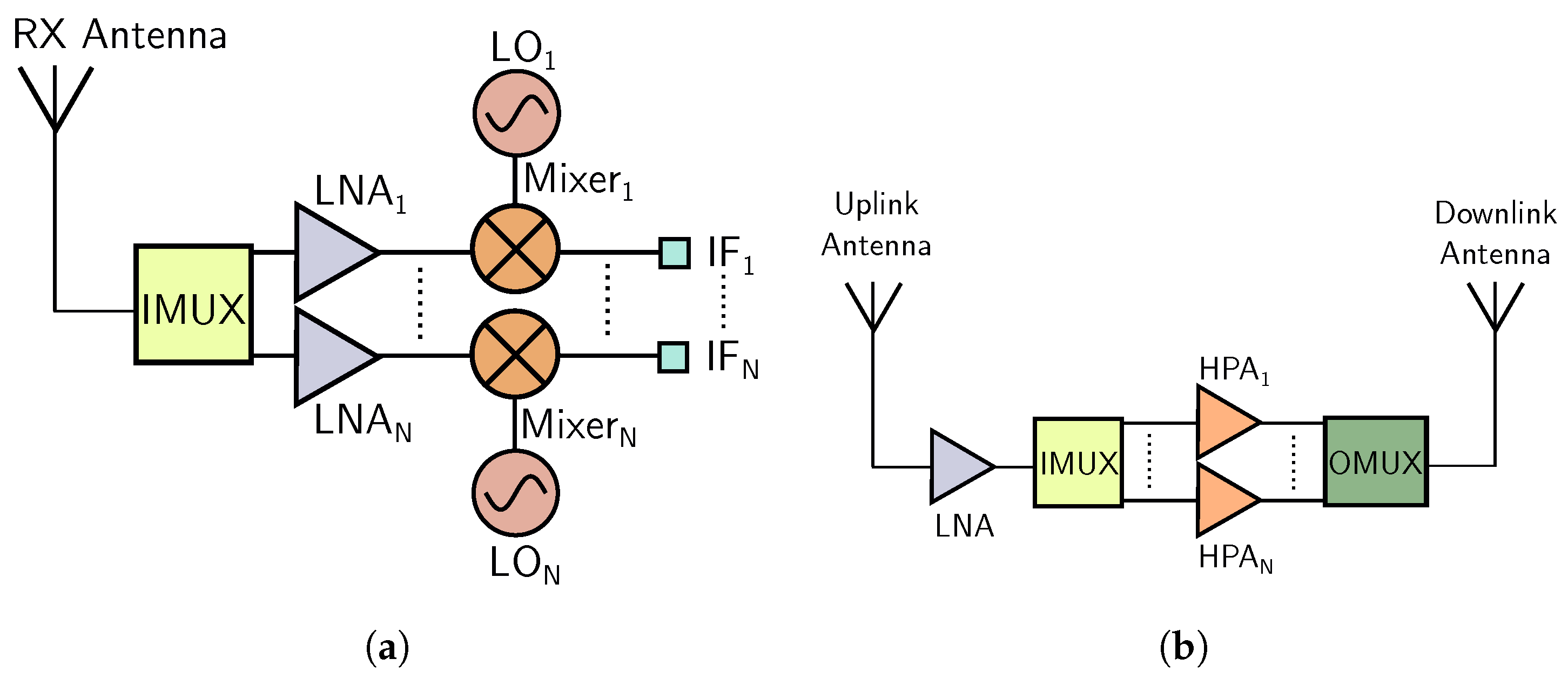
2. State-of-the-Art
3. Algorithms
3.1. Dielectric Resonator Aspect Ratio
3.2. Quality Factor and Bandwidth Formulation
3.3. Coupling Matrix
3.4. Group Delay and Phase Delay Formulation
3.5. Input and Output Coupling Formulation
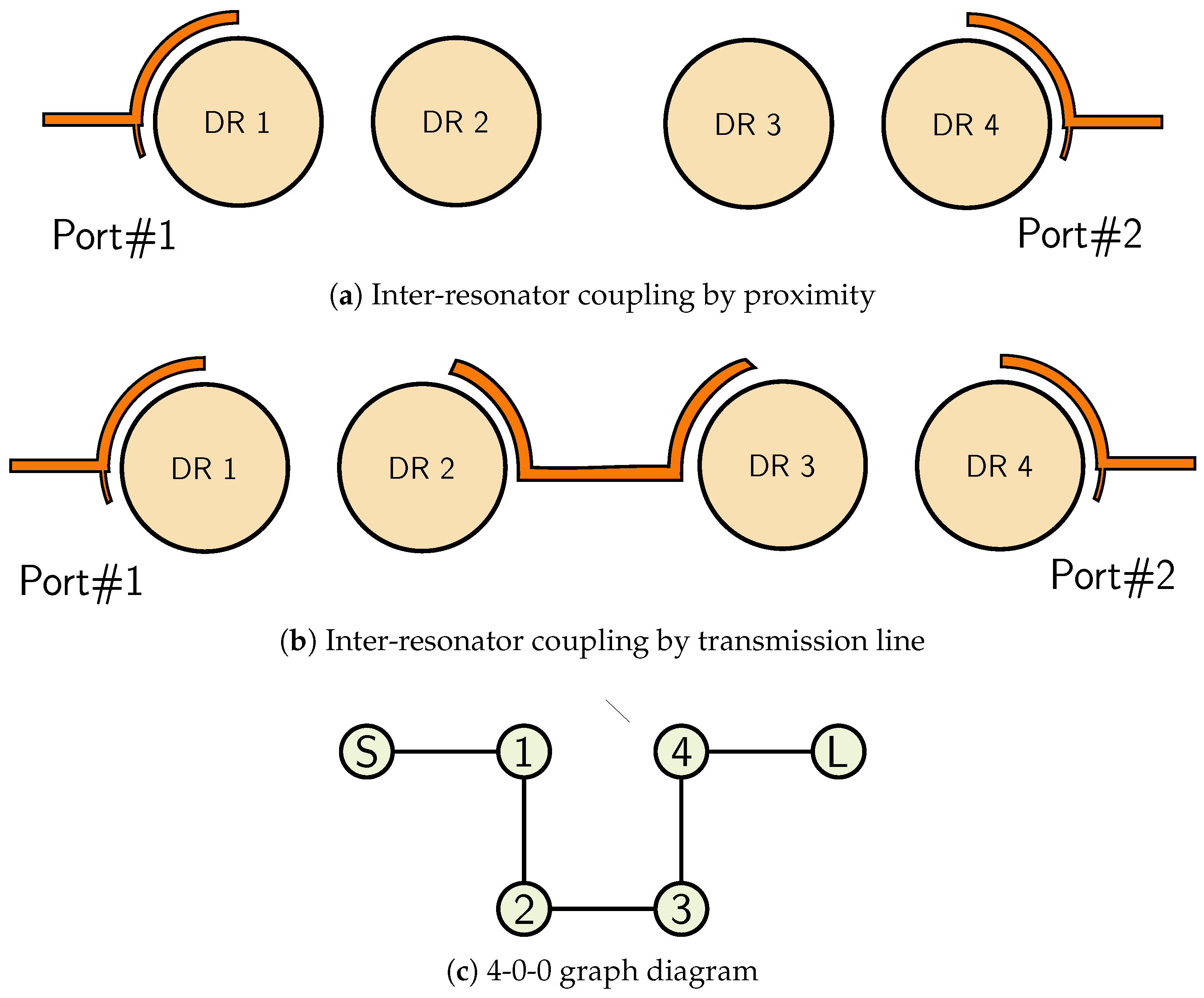
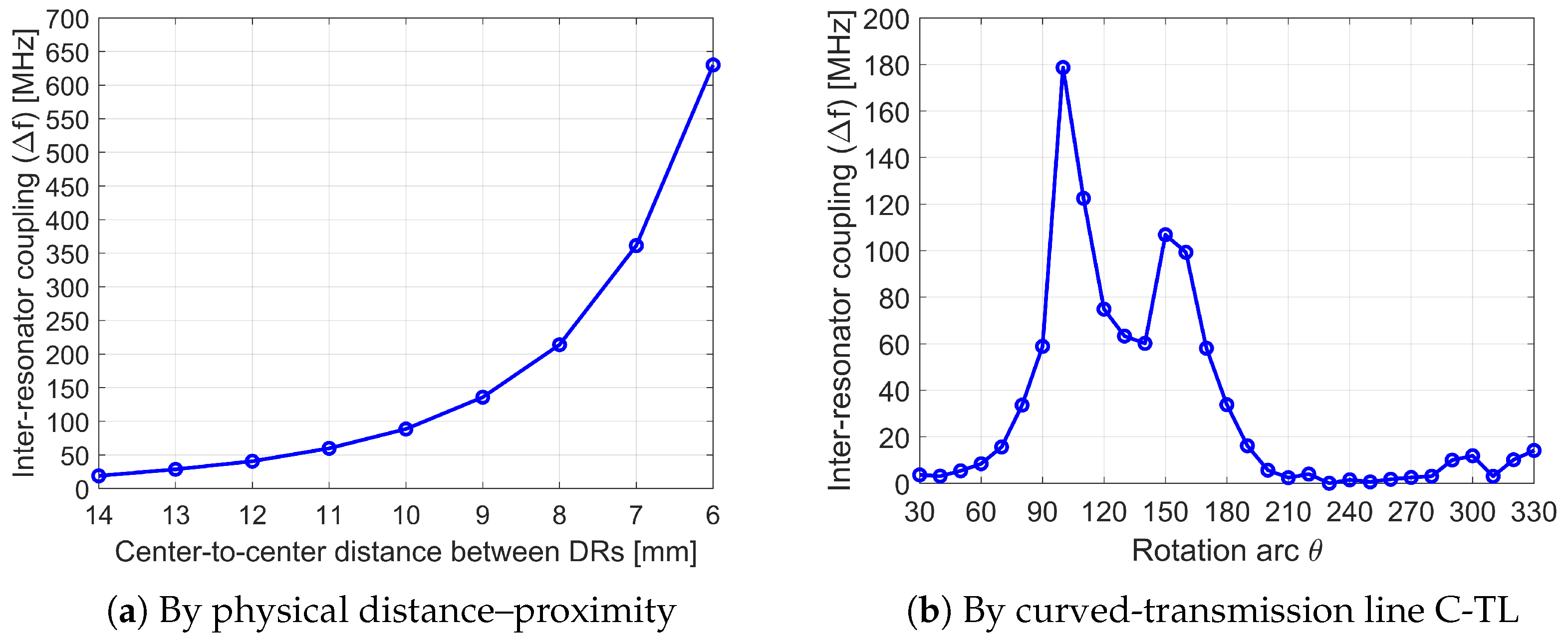
3.6. Inter-Resonator Coupling Formulation
4. Design and Electrical Performance Characterization
4.1. Design Procedure
- Eigen-mode frequency and intrinsic quality factor analyses:An eigen-mode frequency analysis and external quality factor () evaluation of the selected resonator were performed in a representative environment incorporating specific boundary conditions. To distinguish between the resonator’s eigen-modes and those of the cavity, the conductivity of the cavity housing was deliberately reduced by four orders of magnitude relative to silver . Specifically, the lateral boundaries were assigned a conductivity of = 1000 S/m, while the top and bottom faces maintained infinite conductivity to preserve a high-quality ground plane and accommodate Z-axis variations in the circular dielectric resonator modes.
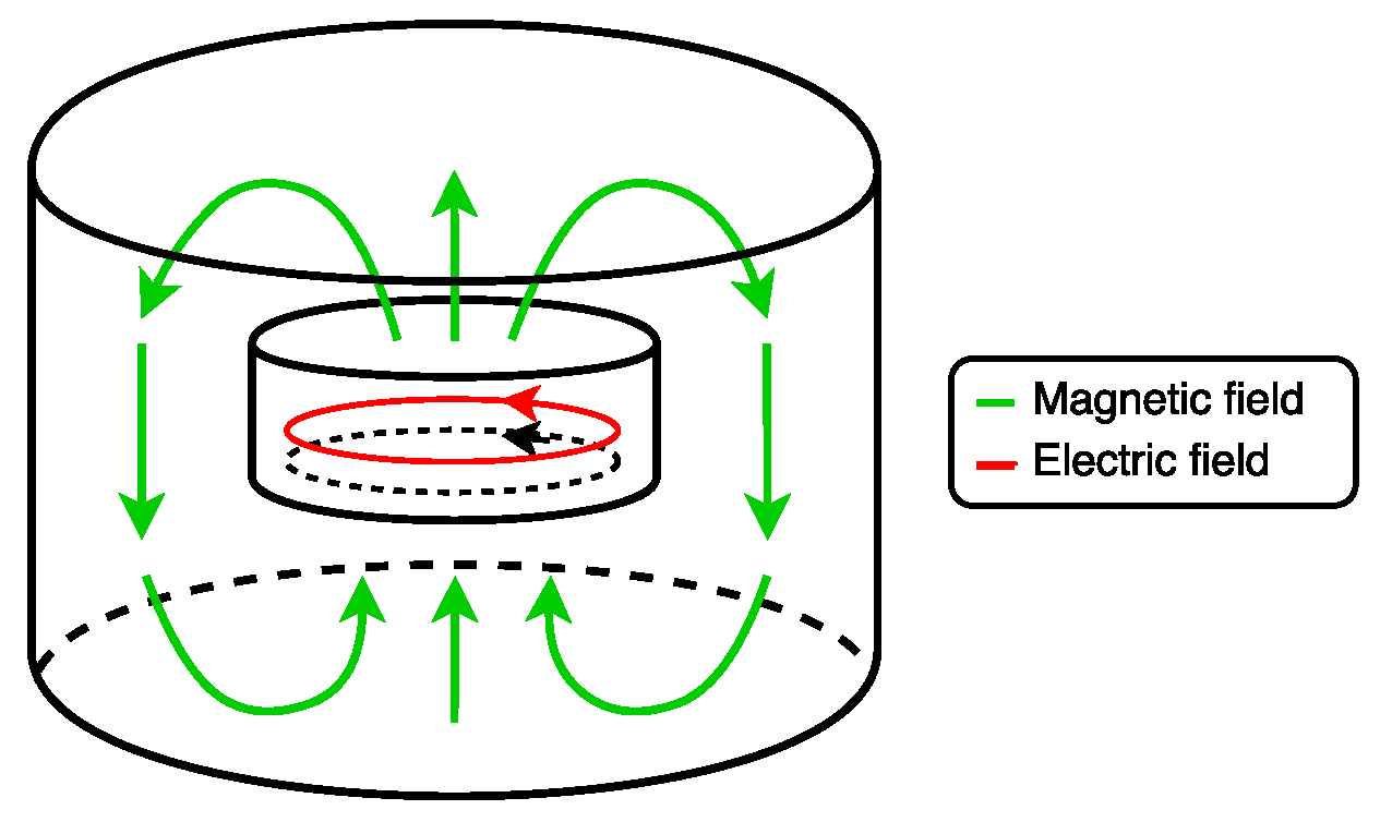
- Resonant mode selection:The cylindrical resonator geometry was chosen to enable the excitation of non-hybrid modes, consistent with typical satellite application requirements [23]. To optimize the operational bandwidth while avoiding unwanted mode interactions, the design employs the resonator’s fundamental mode. This mode selection specifically maximizes the fundamental mode’s single-mode bandwidth, ensuring a spurious-free frequency response.
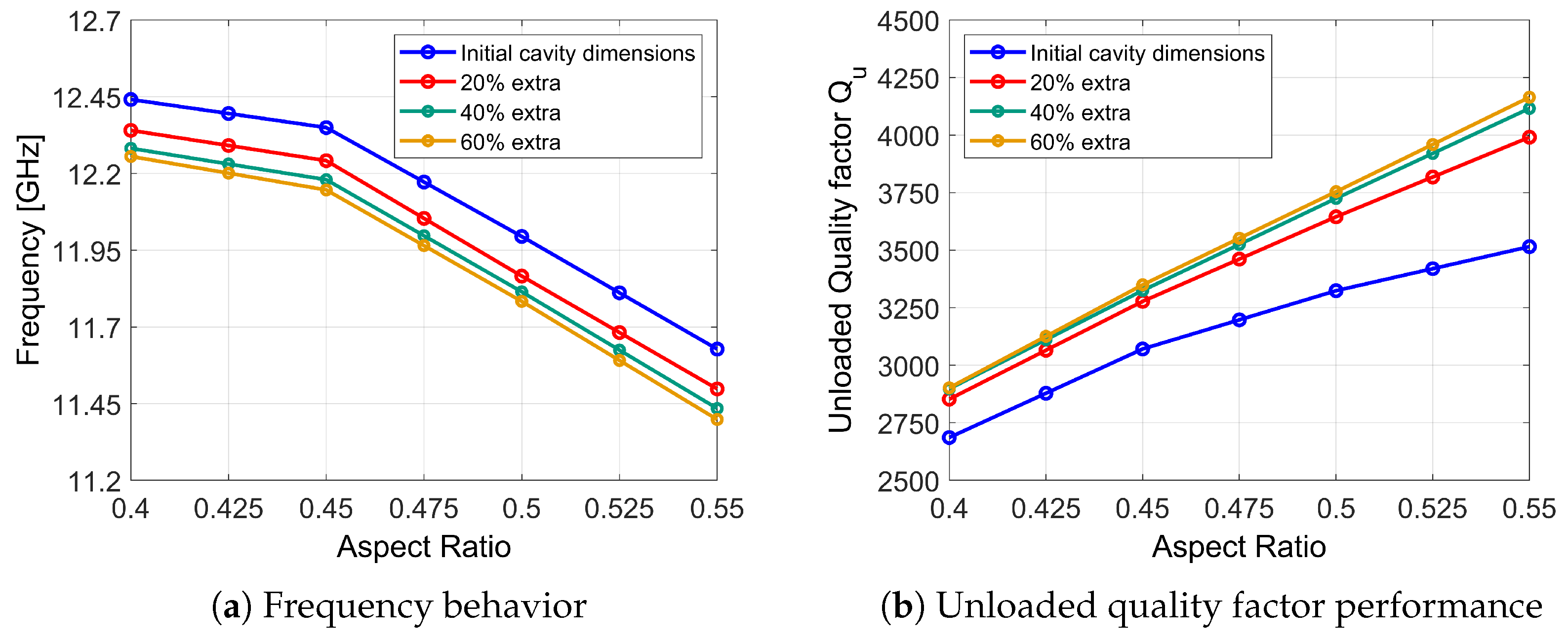
- Parametric analysis of the dielectric resonator aspect ratio and boundary conditions:A parametric study of the resonator’s aspect ratio (AR) was conducted to evaluate its behavior and identify the optimal design point for maximizing the quality factor when implemented on Rogers-family substrates. Additionally, the minimum distance between the resonator and lateral boundaries was systematically varied to ensure a robust design with minimal sensitivity to boundary effects. This methodology maintains consistent resonant frequency and performance characteristics while preventing unwanted cavity-mode excitation. The cavity height was fixed to allow for manual frequency tuning.
- Input–output coupling and inter-resonator coupling characterization:Various feeding methods for exciting the target mode (input–output coupling) were evaluated. After identifying the optimal configurations, their performance was thoroughly characterized across multiple parameters. In parallel, inter-resonator coupling techniques were investigated and parametrically analyzed to determine the nominal operating point (NOP).
- Cross-coupling characterization:The final design stage involves analyzing cross-coupling mechanisms to synthesize complex filter responses, incorporating transmission zeros and/or frequency response equalization techniques.
4.2. Configuration Set-Up, and Identification of Materials and Their Electrical Performance
4.2.1. Setup of Analysis
4.2.2. Identification of Materials and Electrical Performance
- A Rogers RO6002 substrate (relative permittivity = 2.94 ± 0.04, = 0.0012 at 10 GHz [32]) with thickness t = 0.254 mm (10 mils).
- Dielectric adhesive Ablebond 8360 with nominal thickness 0.15 mm and ≈ 3–6, and = 0.005–0.01 (1–10 GHz)—electrical properties not specified in the datasheets. The Q-factor method (detailed in Section 3.5 and Section 3.6) enables characterization via comparison between standalone and bonded DR configurations, though variations occur due to manual application preventing substrate overflow.
- A cavity with height h = 7 mm (arbitrary lateral dimensions), featuring lateral boundaries of conductivity = 1000 S/m and Perfect Electric Conductor (PEC) conditions for both bottom and top boundaries.
4.3. Mode Selection
- Dielectric losses from the resonator substrate.
- Losses originating from the bonding material.
- Non-radiative contributions independent of external loading.
Quality Factor Enhancement
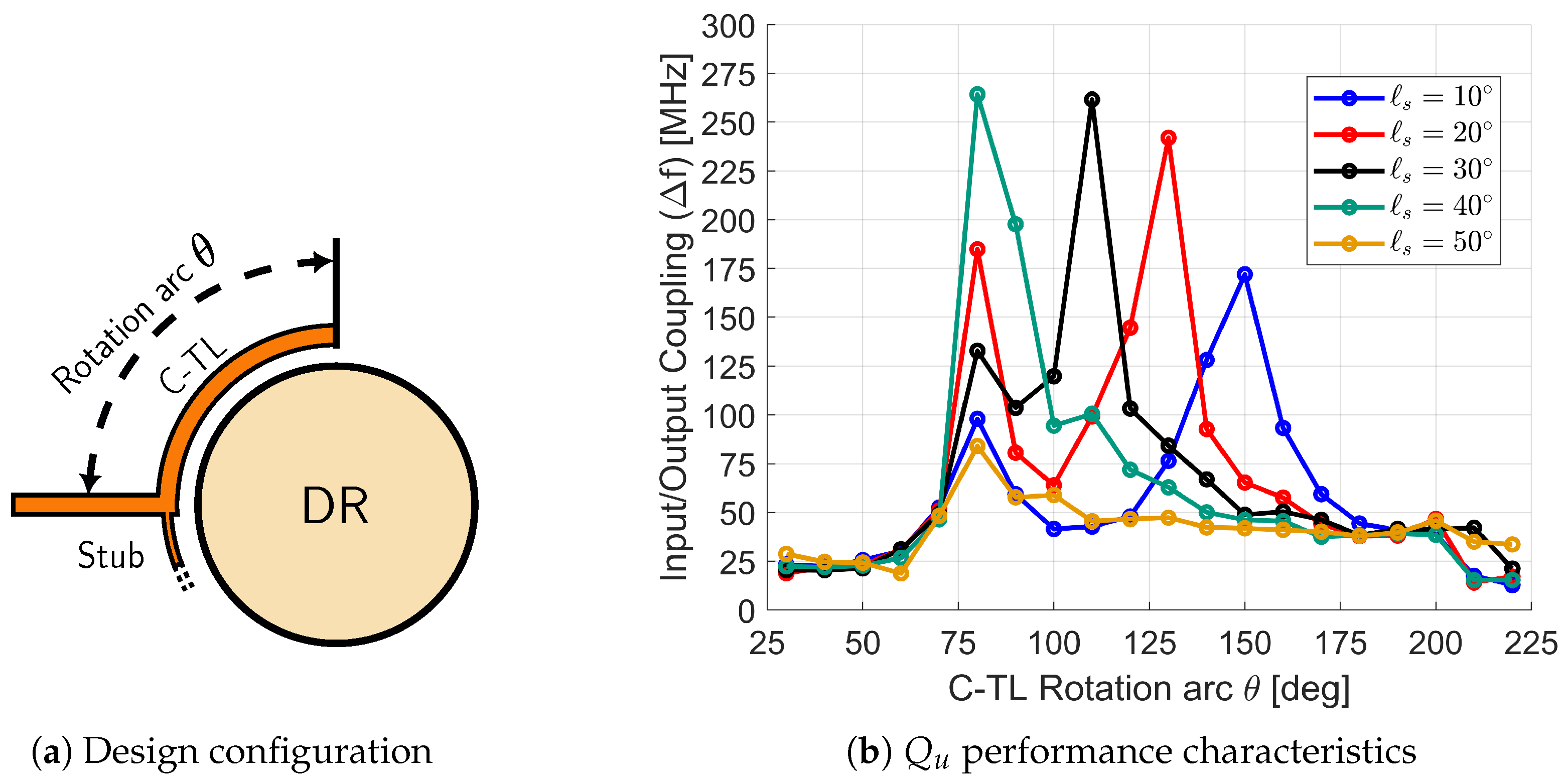
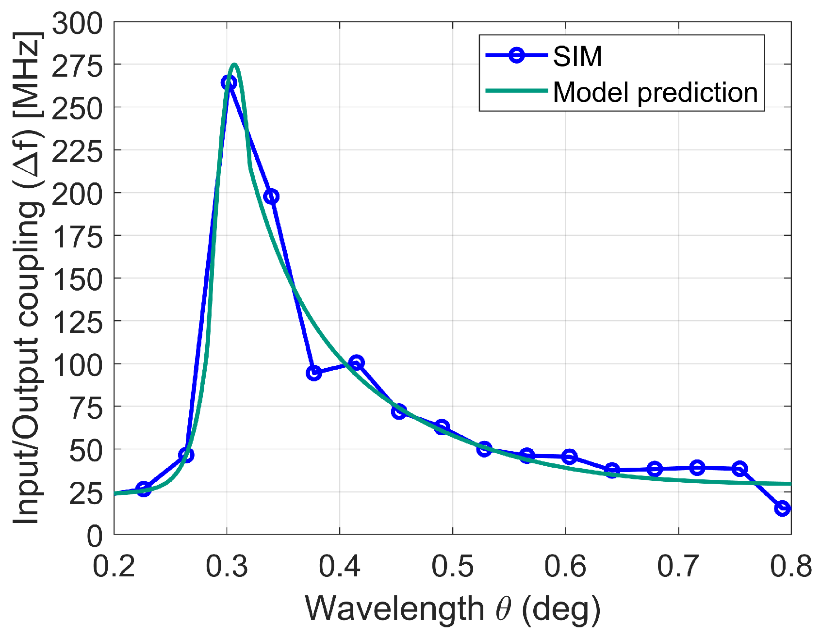
4.4. Input, Inter-Resonator, and Output Coupling Characterization
4.4.1. Input and Output Coupling
- : Spatial frequency of coupling variation (related to the effective propagation constant).
- , : Linear and quadratic attenuation coefficients accounting for radiation and dielectric losses.
- , , n: Coefficients which characterize near-field reactive coupling.
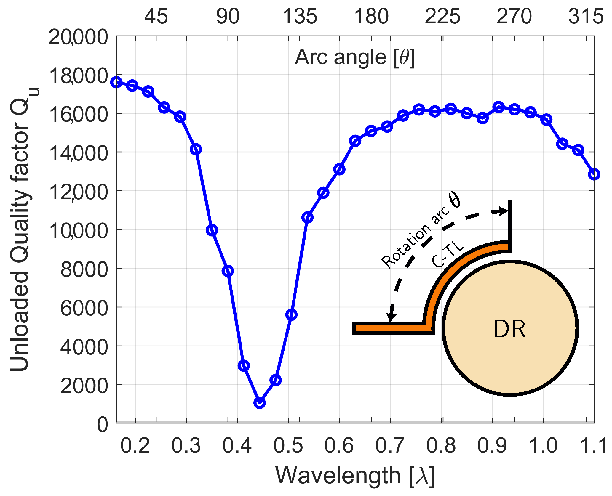
- , , and describe the periodic re-coupling effects, as shown in Figure 14.
- and model the dominant loss mechanism in this region.
- represents the asymptotic unloaded quality factor at large values
4.4.2. Inter-Resonator Coupling
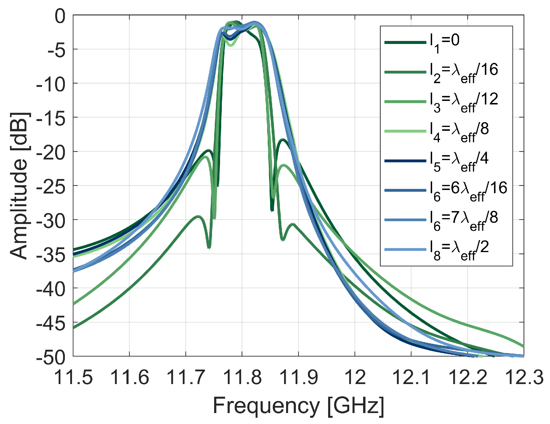
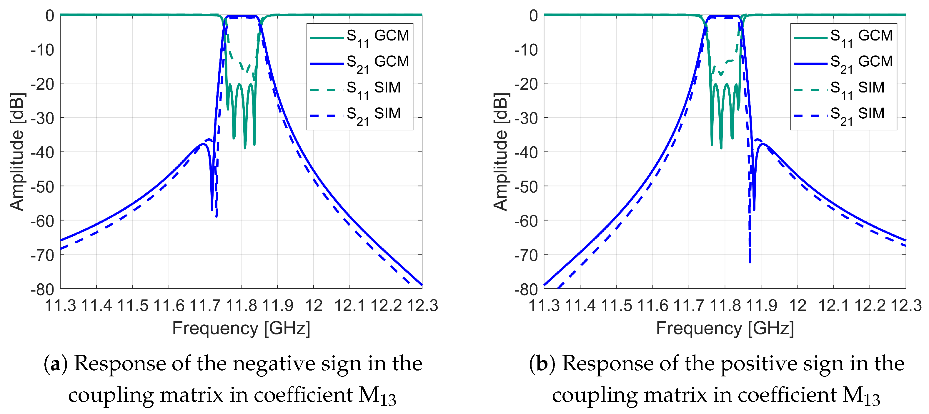
4.4.3. Transmission and Equalization Zeros’ Characterization
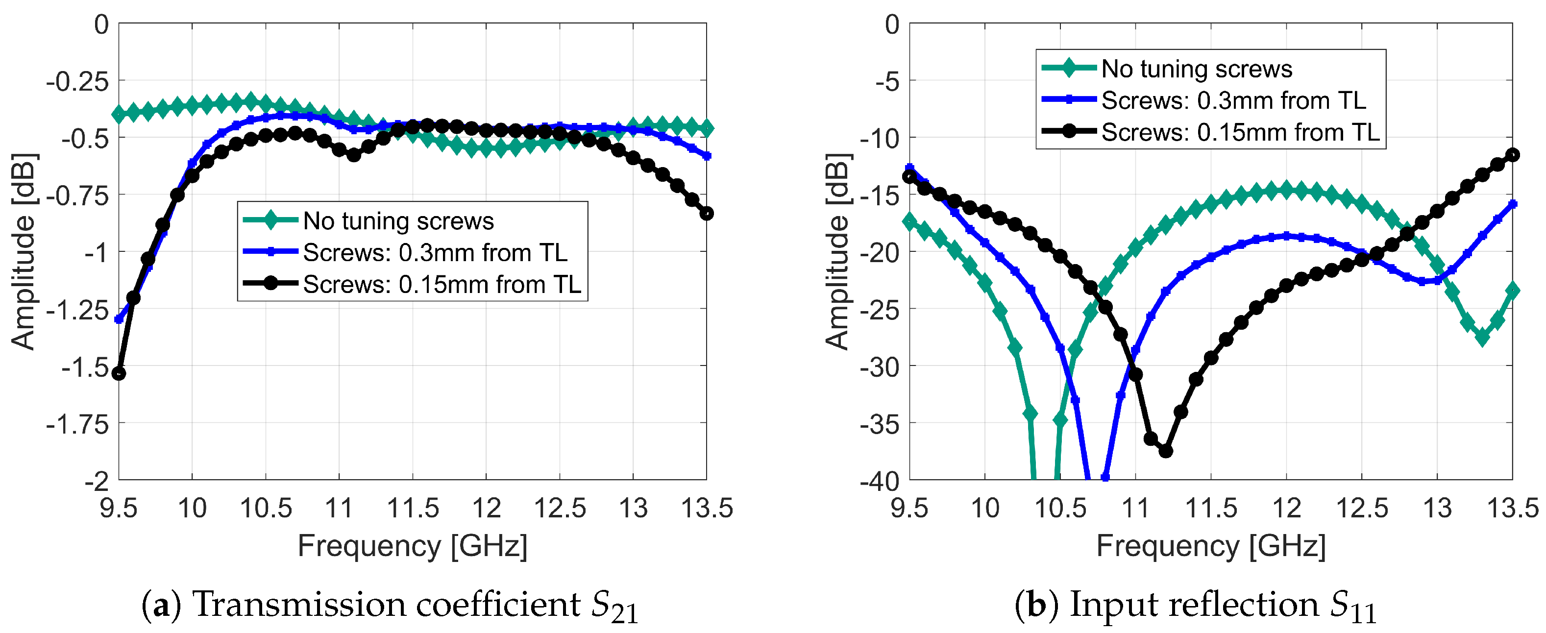
4.4.4. Mechanical Adjustment
5. Filter Design, Simulation, and Experimental Results
- Center frequency = 11.8 GHz.
- Bandwidth BW = 60 MHz.
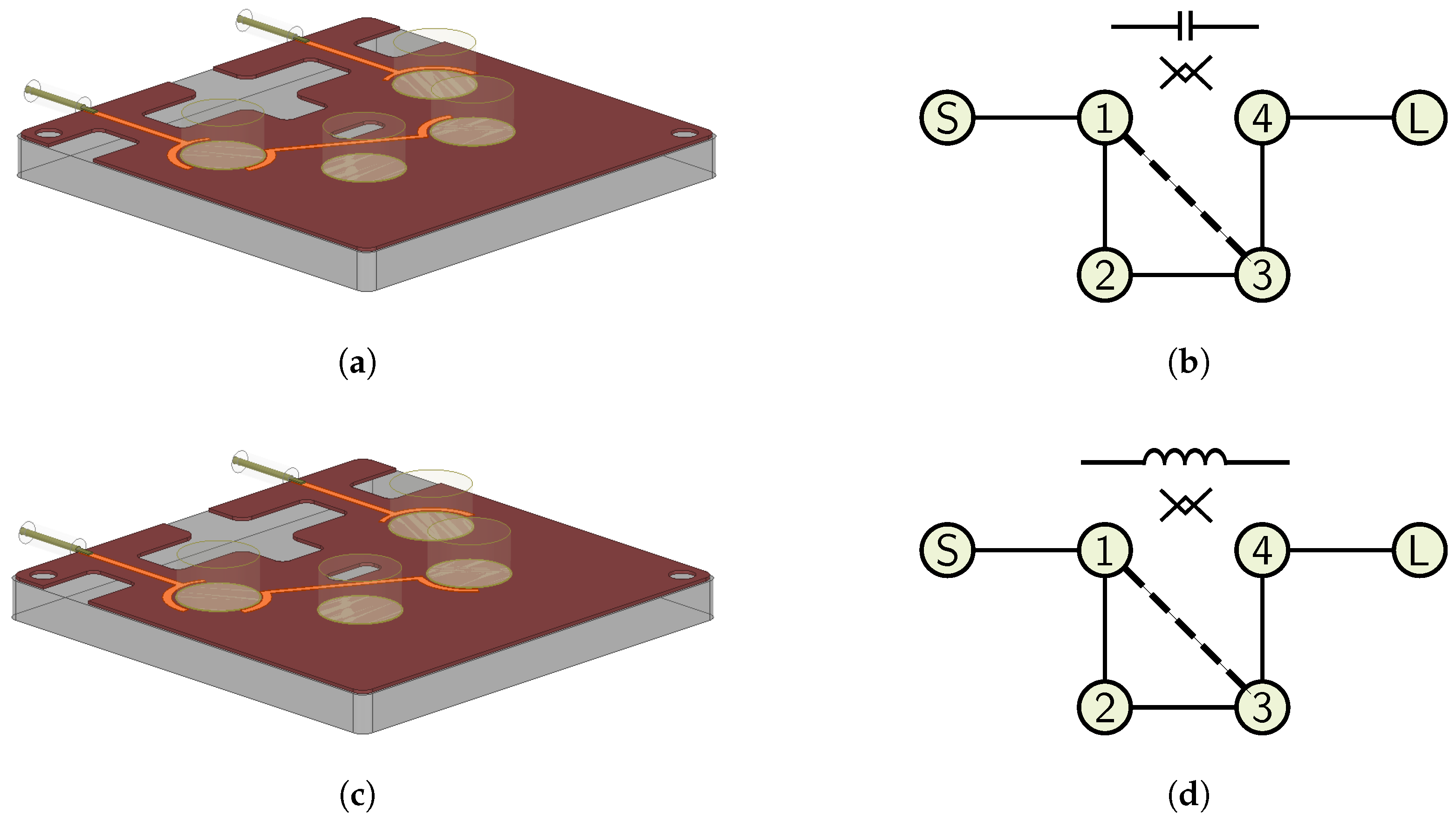
- Filter topologies implementing either of the following:
- –
- Transmission zeros (4-2-0 configuration).
- –
- Equalization zeros (4-0-2 configuration).
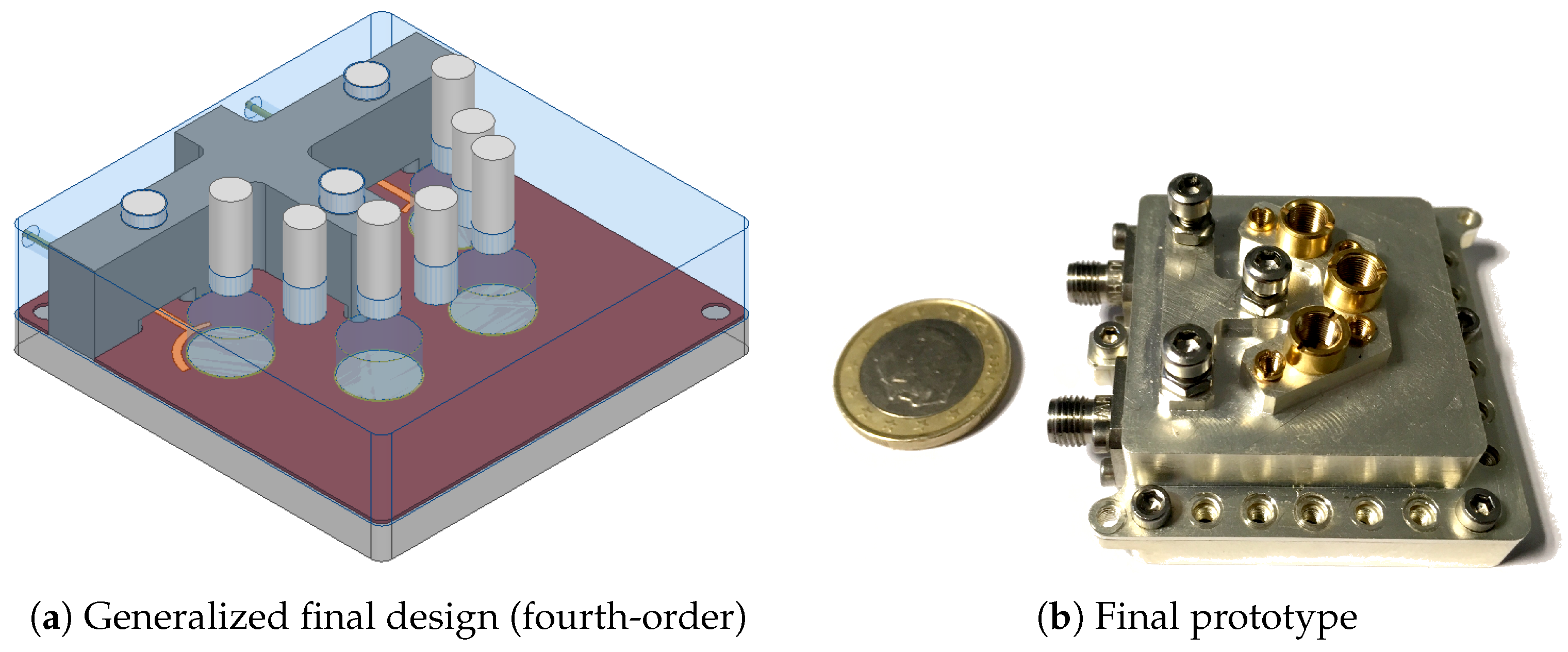
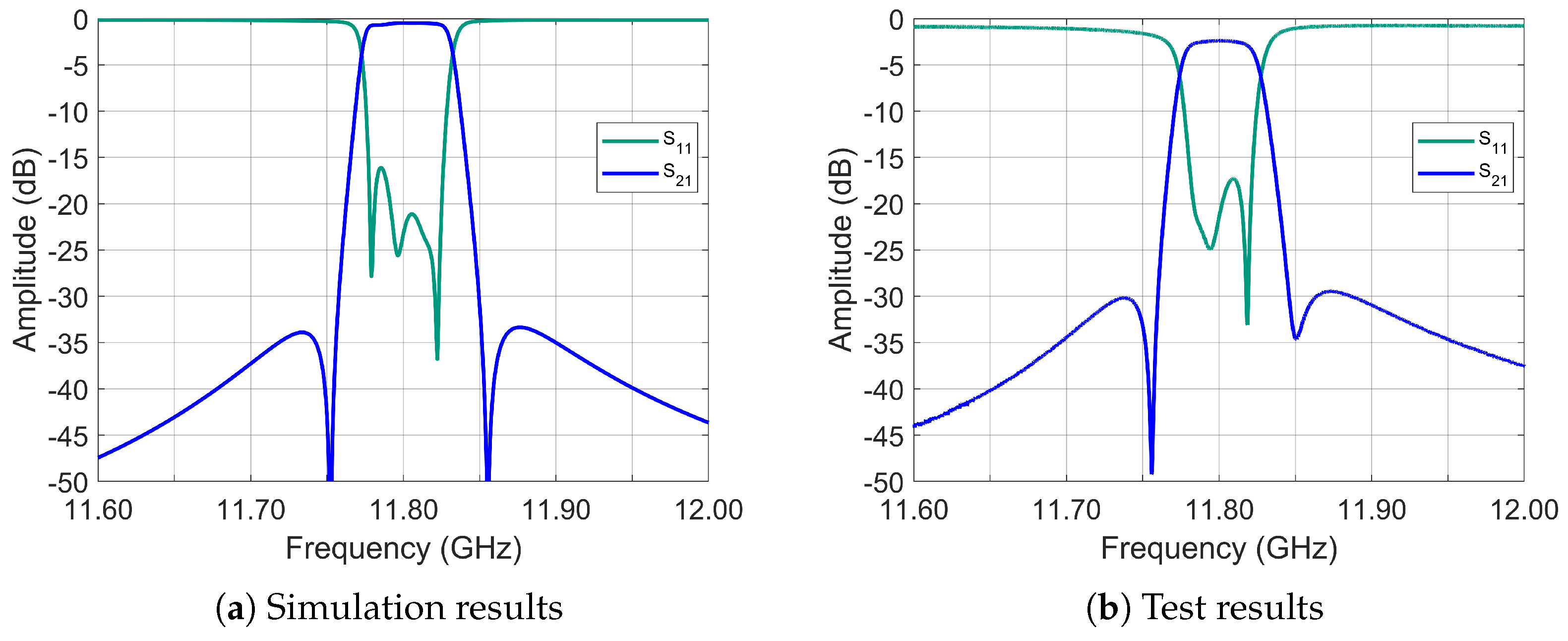
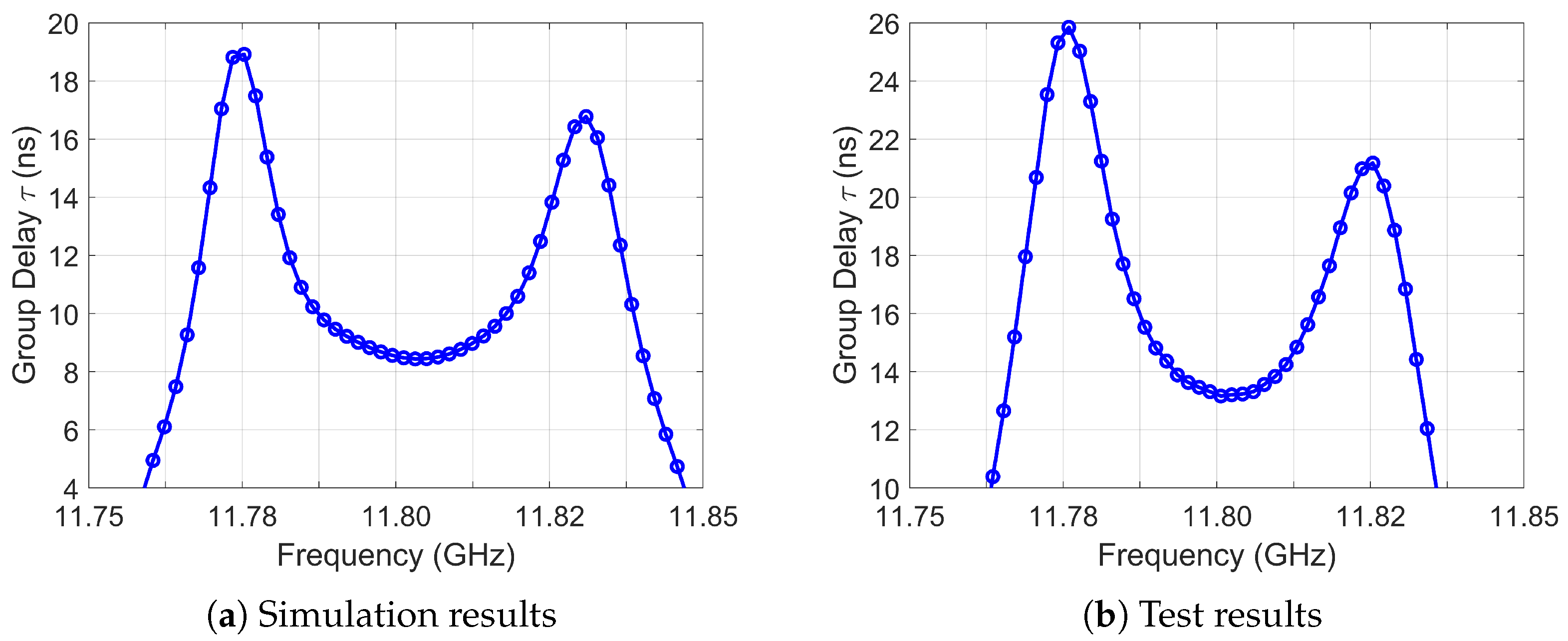
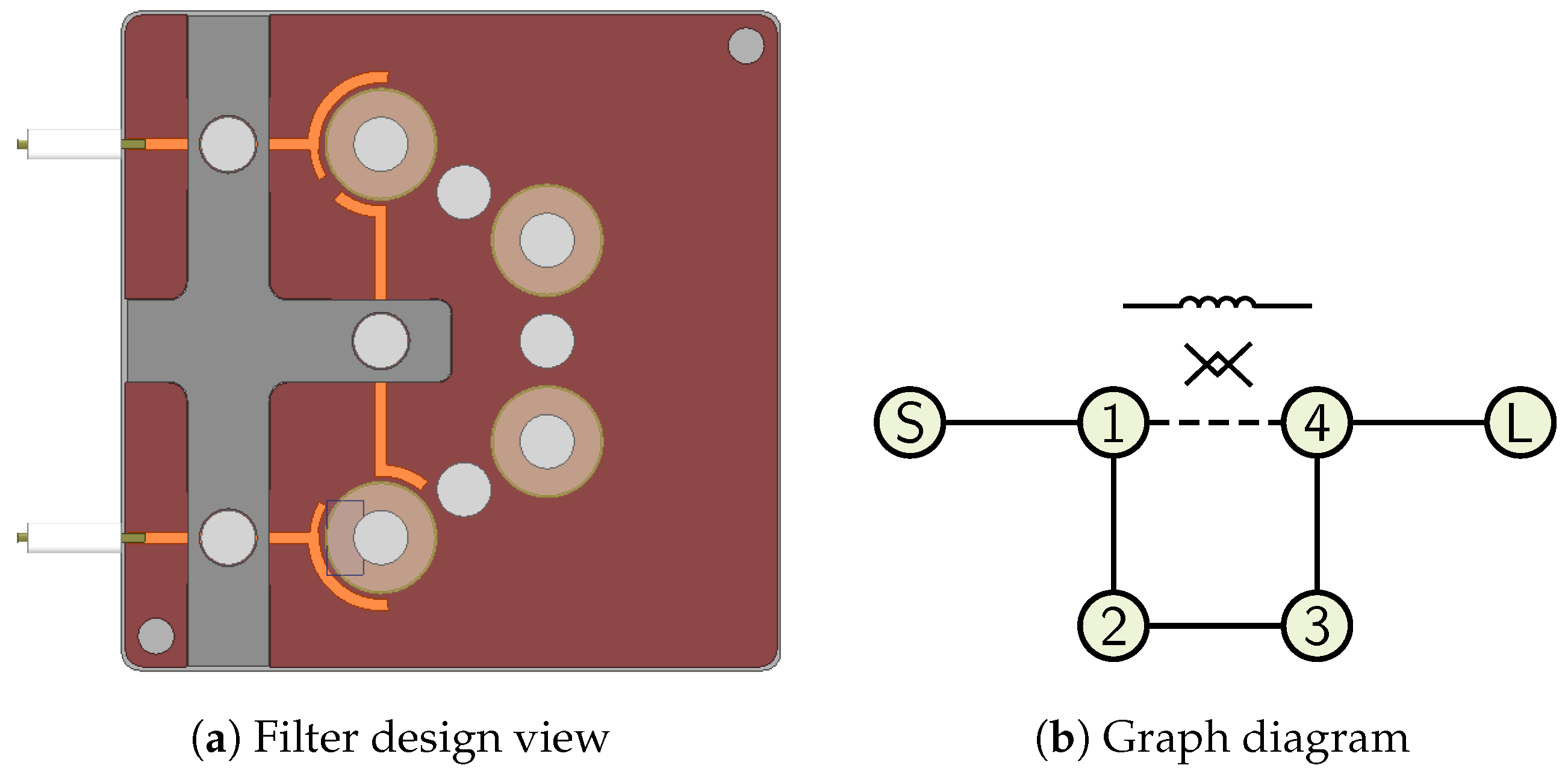
5.1. Filter Design, 4-2-0 Topology
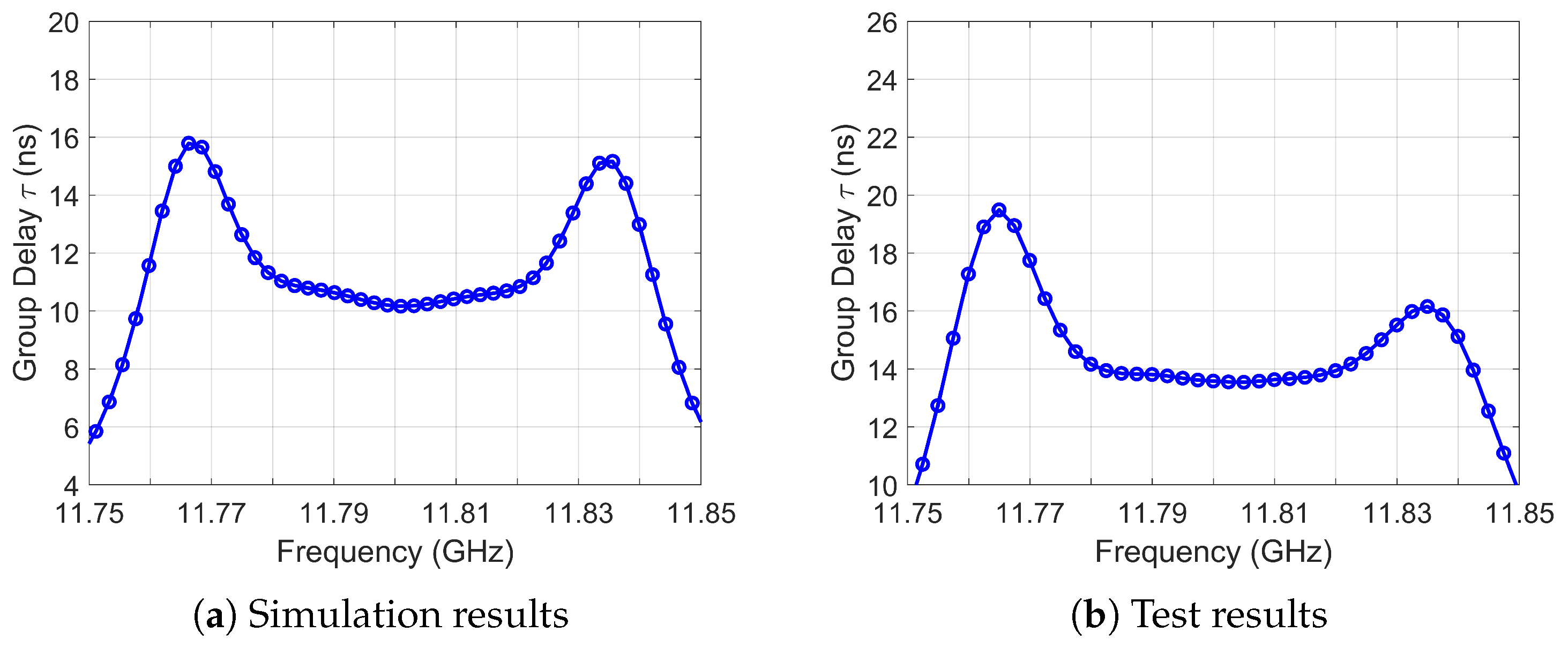
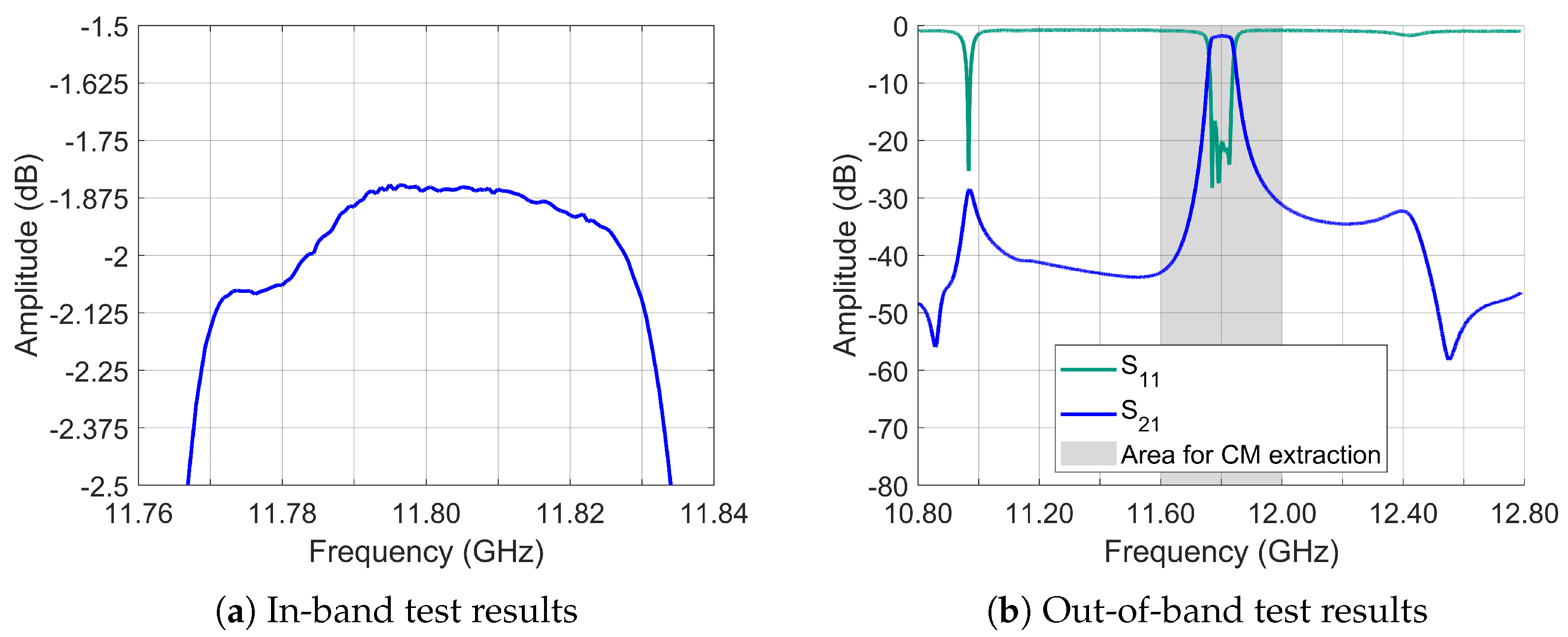
5.2. Filter Design, 4-0-2 Topology
6. Conclusions
7. Future Lines
Author Contributions
Funding
Data Availability Statement
Acknowledgments
Conflicts of Interest
References
- Pellaco, L.; Singh, N.; Jaldén, J. Spectrum Prediction and Interference Detection for Satellite Communications. arXiv 2019, arXiv:1912.04716. [Google Scholar]
- Latif, M.; Salfi, A.U. Design of 5-channel C-band input multiplexer for communication satellites. J. Space Technol. 2015, 5, 40–46. Available online: https://www.researchgate.net/publication/328812628_Design_of_5-Channel_C-Band_Input_Multiplexer_for_Communication_Satellites (accessed on 6 April 2025).
- Monzello, R.C. Unifying G/T and noise figure metrics for receiver systems. In Proceedings of the 2020 Antenna Measurement Techniques Association Symposium (AMTA), Newport, RI, USA, 2–5 November 2020; pp. 1–4. [Google Scholar]
- Lucix Corporation. Space-Qualified Multiplexers. Available online: https://lucix.com/space-passive/multiplexers/ (accessed on 6 April 2025).
- Cameron, R.J.; Kudsia, C.M.; Mansour, R.R. Microwave Filters for Communication Systems: Fundamentals, Design and Applications; Wiley-Interscience: Hoboken, NJ, USA, 2007. [Google Scholar]
- Yu, M.; Tang, W.-C.; Malarky, A.; Dokas, V.; Cameron, R.; Wang, Y. Predistortion technique for cross-coupled filters and its application to satellite communication systems. IEEE Trans. Microw. Theory Tech. 2003, 51, 2505–2515. [Google Scholar] [CrossRef]
- Galaz, J.S.; del Pino, A.P.; Iglesias, P.M. High Order RF Filters for Communications Satellite Systems. In Proceedings of the 6th CNES/ESA International Workshop on Microwave Filters, Toulouse, France, 23–25 March 2015. [Google Scholar]
- Steffè, W.; Vitulli, F. Multilayer Metallic Filters for Q/V Band IMUX. Int. J. Microw. Wirel. Technol. 2022, 14, 362–368. [Google Scholar] [CrossRef]
- Hsieh, L.-H.; Chang, K. Tunable microstrip bandpass filters with two transmission zeros. IEEE Trans. Microw. Theory Tech. 2003, 51, 520–525. [Google Scholar] [CrossRef]
- Huang, X.; Caron, M. Type-based group delay equalization technique. IEEE Trans. Circuits Syst. I Reg. Pap. 2011, 58, 1661–1670. [Google Scholar] [CrossRef]
- Zrigui, N.; Majdy, L.; Zenkouar, L. Regulations Solution of Planar Superconductive Resonators Used in the IMUX Filters of a Communications Satellite Payload in Band C. Power 2014, 4, 6. [Google Scholar]
- Le, T.-H.; Zhu, X.-W.; Ge, C.; Duong, T.-V. A novel diplexer integrated with a shielding case using high Q-factor hybrid resonator bandpass filters. IEEE Microw. Wirel. Compon. Lett. 2018, 28, 215–217. [Google Scholar] [CrossRef]
- Karimzadeh-Jazi, R.; Honarvar, M.A.; Khajeh-Khalili, F. High Q-factor narrow-band bandpass filter using cylindrical dielectric resonators for X-band applications. Prog. Electromagn. Res. Lett. 2018, 77, 65–71. [Google Scholar] [CrossRef]
- Chu, Q.-X.; Ouyang, X.; Wang, H.; Chen, F.-C. TE01δ-mode dielectric-resonator filters with controllable transmission zeros. IEEE Trans. Microw. Theory Tech. 2013, 61, 1086–1094. [Google Scholar] [CrossRef]
- Chen, J.-X.; Zhan, Y.; Qin, W.; Bao, Z.-H. Design of high-performance filtering balun based on TE01δ-mode dielectric resonator. IEEE Trans. Ind. Electron. 2017, 64, 451–458. [Google Scholar] [CrossRef]
- Wang, C.; Zaki, K.A. Dielectric Resonators and Filters, 1st ed.; Wiley-IEEE Press: Hoboken, NJ, USA, 2001. [Google Scholar]
- Sparagna, S.M. L-band dielectric resonator filters and oscillators with low vibration sensitivity and ultra low noise. In Proceedings of the 43rd Annual Symposium on Frequency Control, Denver, CO, USA, 31 May–2 June 1989; pp. 94–106. [Google Scholar] [CrossRef]
- Ain, M.F.; Ahmad, Z.A.; Othman, M.A.; Zubir, I.A.; Hutagalung, S.D.; Sulaiman, A.A.; Othman, A. X-band dielectric resonator bandpass filter. In Proceedings of the 2010 International Conference on Computer Applications and Industrial Electronics, Kuala Lumpur, Malaysia, 15–17 June 2010; pp. 406–410. [Google Scholar]
- Liang, E.C. An Overview of High Q TE Mode Dielectric Resonators and Applications. Ph.D. Thesis, Department of Electronic Engineering, University of California, Los Angeles, CA, USA, 2015. [Google Scholar]
- Fiedziuszko, S.J.; Holmes, S. Dielectric resonators raise your high-Q. IEEE Microw. Mag. 2001, 2, 50–60. [Google Scholar] [CrossRef]
- Mansour, R.R. High-Q tunable dielectric resonator filters. IEEE Microw. Mag. 2009, 10, 84–98. [Google Scholar] [CrossRef]
- Norman, A.; Das, S.; Rohr, T.; Ghidini, T. Advanced manufacturing for space applications. CEAS Space J. 2023, 15, 1–6. [Google Scholar] [CrossRef]
- Liu, Y.; Tomassoni, C.; Jiang, S. Dual-band dielectric resonator filters employing TE01δ mode and degenerate HEH11 modes. IEEE J. Microw. 2023, 3, 1212–1221. [Google Scholar] [CrossRef]
- Xue, Q.; Jin, J.-Y. Bandpass filters designed by transmission zero resonator pairs with proximity coupling. IEEE Trans. Microw. Theory Tech. 2017, 65, 4103–4110. [Google Scholar] [CrossRef]
- Getsinger, W.J. Microstrip dispersion model. IEEE Trans. Microw. Theory Tech. 1973, 21, 34–39. [Google Scholar] [CrossRef]
- Massoni, E.; Bozzi, M.; Perregrini, L.; Tamburini, U.A.; Tomassoni, C. A novel class of high dielectric resonator filters in microstrip line technology. In Proceedings of the 2017 IEEE MTT-S International Microwave Workshop Series on Advanced Materials and Processes for RF and THz Applications (IMWS-AMP), Pavia, Italy, 20–22 September 2017; pp. 1–3. [Google Scholar] [CrossRef]
- Bohra, H.; Prajapati, G. Microstrip filters: A review of different filter designs used in ultrawide band technology. Makara J. Technol. 2020, 24, 5. [Google Scholar] [CrossRef]
- Pozar, D.M. Microwave Engineering, 4th ed.; Wiley: Hoboken, NJ, USA, 2011. [Google Scholar]
- Cameron, R.J. General coupling matrix synthesis methods for Chebyshev filtering functions. IEEE Trans. Microw. Theory Tech. 1999, 47, 433–442. [Google Scholar] [CrossRef]
- Maruwa Co. Microwave Dielectric Ceramics. 2025. Available online: https://www.maruwa-g.com/e/products/ceramic/powdery-molding-goods-1.html (accessed on 4 April 2025).
- Pospieszalski, M.W. Cylindrical dielectric resonators and their applications in TEM line microwave circuits. IEEE Trans. Microw. Theory Tech. 1979, 27, 233–238. [Google Scholar] [CrossRef]
- Rogers Corporation. RT/Duroid 6002 Laminates. Available online: https://www.rogerscorp.com/advanced-electronics-solutions/rt-duroid-laminates/rt-duroid-6002-laminates (accessed on 6 April 2025).
- Khan, U.M. Dual Polarized Dielectric Resonator Antennas; Chalmers University of Technology: Göteborg, Sweden, 2010. [Google Scholar]
- Kajfez, D.; Guillon, P. Dielectric Resonators; Artech House: Norwood, MA, USA, 1990. [Google Scholar]
- Wu, Y.; Gajaweera, R.; Everard, J. Dual-band bandpass filter using TE01δ mode quarter cylindrical dielectric resonators. In Proceedings of the 2016 Asia-Pacific Microwave Conference (APMC), New Delhi, India, 5–9 December 2016; pp. 1–4. [Google Scholar]
- Ouyang, X.; Wang, B.-Y. Inline TE01δ-mode dielectric-resonator filters with controllable transmission zero for wireless base stations. Prog. Electromagn. Res. Lett. 2013, 38, 101–110. [Google Scholar] [CrossRef]
- Awasthi, S.; Biswas, A.; Akhtar, M.J. Dual-band dielectric resonator bandstop filters. Int. J. RF Microw. Comput.-Aided Eng. 2015, 25, 282–288. [Google Scholar] [CrossRef]


| Parameter | DRCF | Microstrip |
|---|---|---|
| Frequency stability | Excellent | Moderate |
| Quality factor (Q) | High | Low |
| Insertion loss | Low | High |
| Size/Envelope | Bulky | Compact |
| Mass | Heavy | Light |
| Manufacturing complexity | High | Low |
| Temperature stability | Lower | Higher |
| Production cost | High | Low |
| Tuning flexibility | Mechanical screws | None |
| Assembly complexity | High | N/A |
| Eigen-Mode Number | Unloaded Quality Factor | Eigen-Mode Frequency (GHz) |
|---|---|---|
| Mode 1 | 86.69 | 10.291 |
| Mode 2 | 651.54 | 10.610 |
| Mode 3 | 651.60 | 10.617 |
| Mode 4 | 2639.34 | 11.401 |
| Mode 5 | 1819.19 | 14.569 |
| Mode 6 | 1830.09 | 14.572 |
| Mode 7 | 2162.55 | 15.105 |
| Mode 8 | 1987.70 | 15.121 |
| Mode 9 | 302.31 | 15.304 |
| Mode 10 | 1741.95 | 16.274 |
| Parameter | Coupling-Based Distance | Coupling-Based TL |
|---|---|---|
| Behavior | Increasing w/frequency | Phase-dependent coupling |
| Max. Coupling (C) | High | Medium |
| Parasitic Influence | Higher | Lower |
| Spurious Modes | N/A | TL mode (Q-TEM) |
| Size | Compact | Compact |
| Parameter | Value/Type |
|---|---|
| Bandwidth (BW) | 45.0 MHz |
| Insertion Loss (IL) | 2.4 dB |
| Quality Factor () | 3000 |
| Return Loss (RL) | 18.0 dB |
| Transmission zeros | −30 dBc |
| Group Delay Variation | 16 ns |
| Tuning Type | Implementation |
| I/O Coupling | C-TL feeder, screw over TL |
| Inter-resonator Coupling | Screw between resonators |
| Frequency Tuning | Screw over resonators |
| TZ Generation | TL (length in multiples of N, ) C-TL arc |
| Parameter | Value/Type |
|---|---|
| Bandwidth (BW) | 60.0 MHz |
| Insertion Loss (IL) | 1.9 dB |
| Quality Factor () | >4000 |
| Return Loss (RL) | 16.5 dB |
| Group Delay Variation | 9 ns |
| Tuning Type | Implementation |
| I/O Coupling | Phase-aligned stubs |
| Inter-resonator Coupling | Iris tuning |
| Frequency Tuning | Screw over resonators |
| EZ Generation | TL (length in multiples of N, ) C-TL arc |
| Frequency Tuning | Capacitive loading screws |
| Parameter | DRCF | MF | DRMF |
|---|---|---|---|
| Frequency stability | Excellent | Moderate | Excellent |
| Q-factor | High | Low | Medium |
| Insertion Loss | Low | High | Medium |
| Size/Envelope | Large | Small | Medium |
| Mass | Heavy | Light | Medium |
| Manufacturing complexity | High | Low | Medium |
| Temperature stability | Excellent | Moderate | Excellent |
| Tuning flexibility | Mechanical | None | Mechanical |
Disclaimer/Publisher’s Note: The statements, opinions and data contained in all publications are solely those of the individual author(s) and contributor(s) and not of MDPI and/or the editor(s). MDPI and/or the editor(s) disclaim responsibility for any injury to people or property resulting from any ideas, methods, instructions or products referred to in the content. |
© 2025 by the authors. Licensee MDPI, Basel, Switzerland. This article is an open access article distributed under the terms and conditions of the Creative Commons Attribution (CC BY) license (https://creativecommons.org/licenses/by/4.0/).
Share and Cite
Espinosa-Adams, D.; Llorente-Romano, S.; González-Posadas, V.; Jiménez-Martín, J.L.; Segovia-Vargas, D. Novel Dielectric Resonator-Based Microstrip Filters with Adjustable Transmission and Equalization Zeros. Electronics 2025, 14, 2557. https://doi.org/10.3390/electronics14132557
Espinosa-Adams D, Llorente-Romano S, González-Posadas V, Jiménez-Martín JL, Segovia-Vargas D. Novel Dielectric Resonator-Based Microstrip Filters with Adjustable Transmission and Equalization Zeros. Electronics. 2025; 14(13):2557. https://doi.org/10.3390/electronics14132557
Chicago/Turabian StyleEspinosa-Adams, David, Sergio Llorente-Romano, Vicente González-Posadas, José Luis Jiménez-Martín, and Daniel Segovia-Vargas. 2025. "Novel Dielectric Resonator-Based Microstrip Filters with Adjustable Transmission and Equalization Zeros" Electronics 14, no. 13: 2557. https://doi.org/10.3390/electronics14132557
APA StyleEspinosa-Adams, D., Llorente-Romano, S., González-Posadas, V., Jiménez-Martín, J. L., & Segovia-Vargas, D. (2025). Novel Dielectric Resonator-Based Microstrip Filters with Adjustable Transmission and Equalization Zeros. Electronics, 14(13), 2557. https://doi.org/10.3390/electronics14132557