Abstract
A millimeter-wave multi-layer and miniaturized multibeam antenna fed by an E-plane Butler matrix (BM) in substrate integrated waveguide (SIW) technology is proposed. For the beam-forming network (BFN), a folded E-plane 4 × 4 BM is proposed, whose basic components are stacked up along the vertical direction aiming to reduce the horizontal size by more than 75% compared with a single-layer BM. For the radiation portion, an unconventional slot antenna array arranged in a ladder type is adopted. The slot antenna elements are distributed in separate layers, making them more compatible with the presented BM and are arranged in the longitudinal direction to suppress the mutual coupling effect. Furthermore, the BM has been adjusted to accommodate the slot antenna array and obtain further miniaturization. The overall dimension of the designed multibeam antenna, taking the BFN into account, is 12 mm × 45 mm × 2 mm (1.2 λ × 4.5 λ × 0.2 λ), which is preferable for future 6G smartphone applications. The impacts of the air gap in fabrication are also taken into consideration to alleviate the error between simulated model and fabricated prototype.
1. Introduction
To adapt to the ever-growing wireless data rate demands and the popularity of smartphones, it is becoming increasingly urgent to seek new ways to increase both wireless performance and capacity, especially in the coming sixth-generation (6G) mobile communication systems. In the past years, most of the preliminary research regarding 5G has focused on two practical technologies. One is massive multi-input multi-output (MIMO) technology, and the other is millimeter-wave (mm-wave) technology. However, for the realization of massive MIMO, the inevitably severe mutual coupling effects between the multiple antennas must be properly addressed in terminal devices with limited space. Compared with the massive MIMO antenna, a multibeam antenna with better angular diversity would be a preferable candidate for 5G/6G smartphone applications [1,2,3].
The key to achieving multibeam radiation is to design the desired beam-forming network (BFN). Among various types of BFNs, including optical-type BFNs and circuit-type BFNs, the Butler matrix (BM) is the most popular one because it has a simpler architecture than an optics-type lens, a higher efficiency than a Blass matrix and a wider bandwidth than a Nolen matrix.
Microstrip-lines and substrate-integrated waveguides (SIWs) are two common transmission-line technologies applied to designing BMs. Operating at sub-mm-wave frequency bands, several BMs in microstrip-line technologies are proposed in [4,5,6,7,8,9]. For the mm-wave applications, however, it cannot be ignored that microstrip-line BFNs suffer from high radiation loss, which will disrupt the unidirectional performance of the radiation pattern. Due to its properties of low transmission loss and ease of integration, SIW becomes a usual approach for electromagnetic wave transmission in mm-wave bands.
A number of BFNs based on SIW technology have recently been presented. Blass matrices, Nolen matrices, BMs, and Rotman lenses built in single-layer SIW are reported in [10,11,12,13,14,15]. Nevertheless, SIW BFN designs encounter a weakness, i.e., the bulky size or large dimension. Facing this issue, one can resort to multi-layer PCB technology, which can be stacked up in the vertical direction to save space. Other than Low Temperature Co-fired Ceramic (LTCC) technology, there are two feasible means for multi-layer PCB integration, i.e., compressive type and adhesive type. The compressive type employs screws to fix and tighten each layer together and the adhesive type applies prepregs to bond separate layers together. Between these two approaches, the compressive type is preferable for its lower cost and better design flexibility. Based on the aforementioned multi-layer fabrication technologies, refs. [16,17,18] have proposed two-layer SIW BFN schemes by implementations of E-plane hybrid couplers or coupling slots to reduce the dimensions. In [19], a four-layer SIW BM scheme is realized by folding a single-layer BM twice. In [20], based on the two-layer SIW BM presented in [16], a compact four-layer SIW BM is developed by folding the SIW such that the longitudinal length can be reduced by half. The schemes proposed in [19,20] both introduce coupling slots to provide layer-to-layer transmissions because of the required folded transmission paths. Nevertheless, the introduced coupling slots suffer from severe energy leakage from the air gap or the bonding-film gap between layers in fabrication unless Low Temperature Co-fired Ceramic (LTCC) technology, which is costly and would restrict the bandwidth of the antenna due to its high permittivity, is adopted. In [21,22], a concept of E-plane 4 × 4 BM is proposed. In [21], such an E-plane BM is combined with an H-plane BM to generate 2D multibeam. In [22], the slot array is stacked above the E-plane BM so that excessive layers of laminated are required, which would contribute to fabrication difficulty and deteriorated fabrication tolerance. Reviewing the state-of-the-art development of multi-layer BM, there is still room for dimension reduction, especially for the compact integration between the BM and the radiation portion.
Facing the above challenges, a miniaturized and compact multibeam antenna with a multi-layer E-plane 4 × 4 BM serving as the BFN is proposed in this paper. As the BFN, a modified four-layer E-plane 4 × 4 BM is proposed in Section 2. Compared with the similar four-layer 4 × 4 BM reported in [20], this design has eliminated any employment of coupling slots to lessen energy leakage and has reduced the occupied area by approximately 47%. How the basic components react to the change in the air gap thickness is analyzed as well, to seek satisfactory consistency between simulated and measured results. In Section 3, a novel arrangement of the slot antenna array is proposed to ensure compatibility with the E-plane BM and suppress the mutual coupling effect. Also, compensating phase shifters are employed to address the deviated angle of the steering beams. In Section 4, with some adjustments, the E-plane 4 × 4 BM is connected to the proposed slot antenna array, and further miniaturization can be obtained. In summary, the main contributions of this paper are as follows.
- (1)
- Presenting a new scheme of folded four-layer 4 × 4 BM with a reduced occupied area without any use of coupling slots.
- (2)
- Analyzing the air gap impact to achieve better agreement between simulated and measured results.
- (3)
- Exploiting an unconventional arrangement of slot antenna array, which is compatible with the BFN whose output ports are distributed in separate layers.
- (4)
- Calibrating the deviated angle of the generated beams with resorting to compensating phase shifters.
- (5)
- Recombining the BFN and the antenna array to miniaturize the multibeam antenna array.
2. E-Plane 4 × 4 Butler Matrix Design
A typical 4 × 4 Butler matrix (BM) is constructed by a series of couplers and phase shifters. Additionally, several crossovers are required to address path crossings. The hybrid couplers can divide the energy equally with a phase difference of ±90°. The phase shifters are inserted to maintain the desired phase gradients at the output ports. For an H-plane BM, these basic components are usually arranged in a horizontal plane, which is common use in the open literature [11,12,13]. With the development of a 3D integration system, the vertical connection and transmission become a key challenge in system design [21]. The E-plane 4 × 4 BM, as a counterpart, consists of similar basic components in a distinguishing combination form. The basic component of the E-plane 4 × 4 BM includes the E-plane couplers, E-plane crossovers, and E-plane phase shifters, which are briefly introduced in [21,22]. On the basis of these results, the detailed structure and design process are elaborated in this paper. Furthermore, to improve performance, the impacts of air gaps are also taken into consideration.
2.1. Topology of E-Plane 4 × 4 BM
As depicted in Figure 1, the E-plane 4 × 4 BM contains E-plane couplers, E-plane crossovers and several phase shifters with fixed values. Unlike typical H-plane designs, the basic components are vertically stacked. Compared to an H-plane BM integrated into such a single layer, the E-plane BM has the ability to allocate the signal into separate layers. By doing so, the separated transmission path can be stacked up with the assistance of the closed structure of SIW, contributing to the size reduction in BM. The detailed design procedures of the basic BM components, including the E-plane coupler and phase shifter are described in [16,20,21,22,23,24,25,26]. The introduced E-plane crossover is structured by two cascaded E-plane hybrid couplers. The E-plane hybrid coupler can produce layer-to-layer coupling transmission by etching two slots on the co-plane of the upper layer and lower layer. Layer-to-layer cross transmission is realized by the implementation of an E-plane crossover. Finally, the structure of the E-plane 4 × 4 BM can be built up by four layers of laminates, each of which contains an input port and an output port.
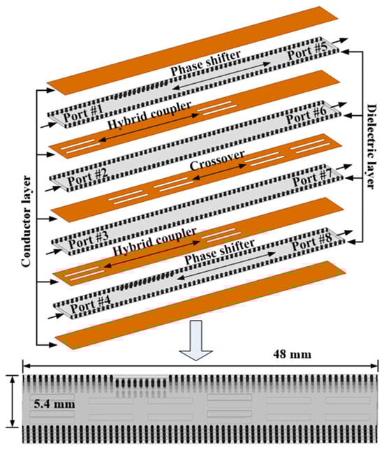
Figure 1.
Configuration of the proposed E-plane 4 × 4 BM.
2.2. Design Consideration
Since compressive type is adopted to deal with this multi-layer structure fabrication, it is of great significance to analyze the performances of the basic components when the thicknesses of the air gap change, so as to lessen the unconformity between the simulated model and fabricated prototype. In other words, how the existent air gap impacts the performances, mainly in terms of transmission coefficients and phase errors, should be taken into account.
In a multi-layer design, there are usually three basic components capable of vertical energy transmission. There are E-plane hybrid couplers, E-plane crossover, and coupling slots. Similarly to the H-plane counterparts, the E-plane hybrid coupler can divide the energy by half and generates a phase difference of ±90°. But two etched slots are required in the common plane of two substrates. For an H-plane coupler, a coupling region is constructed to support a higher-order mode, which is necessary for coupler design. For an E-plane coupler, the etched slots can help generate a coupling region to support TEM mode, which is essential for phase difference generation. The E-plane crossover can be conveniently obtained by cascading two E-plane couplers. The coupling slot is an effective method for vertical transmission between layers, since it can cut the surface current of SIW. The side views of three basic components are presented in Figure 2. In this figure, the thickness of the air gap is denoted as t. Referring to our former fabrication experiences, the thickness of the air gap can vary from 0.02 mm to 0.08 mm in most cases, which can be estimated by measuring the thicknesses of multi-layer structures and single-layer structures, respectively, by using a Vernier Caliper.
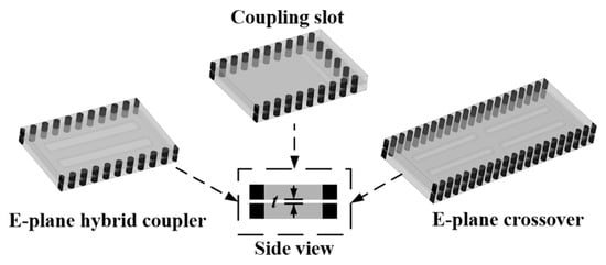
Figure 2.
Side views of the E-plane hybrid coupler, E-plane crossover, and coupling slot.
As a reference, t = 0.05 mm is taken as an initial value to optimize the performance of E-plane hybrid couplers, E-plane crossovers, and the coupling slot implemented by High Frequency Electromagnetic Field Simulation software 2020. Next, the parametric sweep of t from 0.02 mm to 0.08 mm is performed to simulate the uncertainty of the thickness of the air gap. The transmission coefficients and phase errors of these components vary with the air gap thicknesses changes which are illustrated in Figure 3a, Figure 3b and Figure 3c, respectively. The phase errors are calculated relative to t = 0.05 mm.
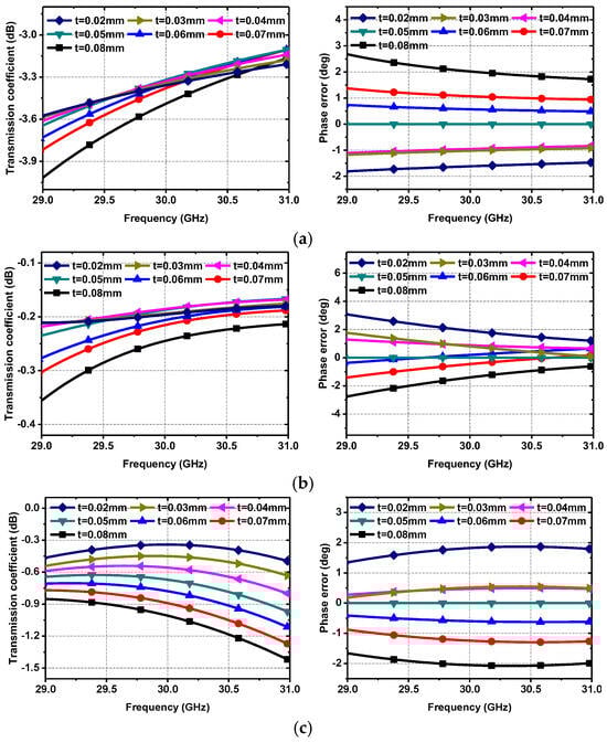
Figure 3.
Transmission coefficients and phase errors related to different t of the (a) E-plane hybrid coupler, (b) E-plane crossover, and (c) coupling slot.
There are two major factors that take charge of the beam steering properties, i.e., the energy magnitude and the phase difference. Derived from Figure 3a,b, smaller fluctuations of transmission coefficients can be observed when t < 0.05 mm compared with when t > 0.05. Based on this characteristic, a bigger initial value of t brings a better error-tolerant rate. However, the produced phase errors corresponding to both t < 0.05 mm and t > 0.05 remain unstable. To summarize, t = 0.05 mm is set as the initial value to balance potential errors of transmission coefficient magnitude and phase difference in the simulation. Similarly, the simulated results of the coupling slot are plotted in Figure 3c. The insert loss reaches up to 1 dB at the center frequency with t = 0.08 mm, which represents that the transmission suffers from 20% energy leakage. Also, with parameter t variance, the coupling slot encounters a considerable magnitude error which restricts the magnitude’s balanced property. In conclusion, a coupling slot should be employed in LTCC technology rather than in compressive type or cohesive type multi-layer PCB technology.
2.3. Superiority
Unlike the folded BM mentioned in [20], the layer-to-layer transmission can be realized in the E-plane 4 × 4 BM without introducing a coupling slot whose performance is very sensitive to the air gap or bonding-film gap between layers in fabrication. The new scheme of 4 × 4 BM is put forward with the E-plane crossovers instead of coupling slots. From the top view, only a single transmission path remained due to the vertically stacked configuration. In other words, the width is reduced by approximately 75% compared with the single-layer BM. The occupied area of the similar four-layer 4 × 4 BM is approximately 2.16 λ × 0.96 λ [20]. When it is cascaded with an antenna array, a transition network is required in [20] to rearrange the output ports, which will extend the occupied area to 2.88 λ × 1.7 λ, while the proposed E-plane 4 × 4 BM covers an area of 4.8 λ × 0.54 λ, so that the occupied area can be reduced by approximately 47%. Also, E-plane 4 × 4 BM maintains the possibility of connecting to an antenna array directly because four output ports are allocated in four separate layers. In addition to the aforementioned properties, and in collaboration with H-plane BM, E-plane BM can manipulate vertical and horizontal amplitude and phase distributions to form a 2D scanning BFN.
2.4. Performance
Performances of the BM are characterized by the following indexes: return loss, isolation and errors of the signal amplitude, and phase difference. The simulated S-parameters with port #1 excitation are shown in Figure 4. The results associated with other ports excitations are similar to those for port #1 excitation. As the figure shows, the reflection coefficients are below −15 dB from 29 GHz to 31 GHz, as well as the isolation coefficients. The transmission coefficients can evaluate the power division and the magnitude balance. It is seen that the amplitude generates ripples of ±0.6 dB, near −6.8 dB. These results indicate an insertion loss of approximately 0.8 dB, which can be verified by the results shown in Figure 3. Well-balanced phase differences between adjacent output ports are shown in Figure 4, i.e., ang(S5P)–ang(S6P), ang(S6P)–(S7P), and ang(S7P)–ang(S8P) are approximately −45°, 135°, −135°, and 45° for excitations from port #1 to #4 (noted as P = 1 to 4), respectively. Within the interested frequency spectrum (29 to 31 GHz), the maximum phase errors are less than ±5°. The simulated results fully confirm the validity of the application of the designed E-plane 4 × 4 BM as the BFN.
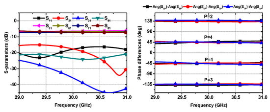
Figure 4.
Simulated S-parameters for port #1 excitation and phase differences in E-plane 4 × 4 BM.
3. Slot Antenna Array Design
Due to its ease of integration and fabrication, a slot antenna is preferable for adoption as the radiation element in SIW technology. Several schemes of latitudinally arranged slot antenna arrays are reported in [11,12,13,18,27]. However, these slot antenna arrays suffer from severe mutual coupling effects, which deteriorates angular diversity, reduces radiation efficiency [28]. To suppress the mutual coupling effect, an unconventional ladder-type longitudinally arranged slot antenna array is presented. Referring to Figure 5, the four slot antenna elements are distributed in four separate layers to accommodate the E-plane 4 × 4 BM whose output ports are distributed in separate layers as well. Furthermore, they are arranged in the longitudinal direction for the purpose of suppressing the surface wave coupling.
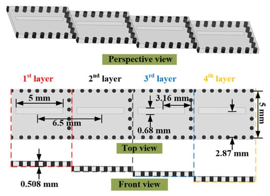
Figure 5.
Perspective view, top view, and front view of ladder-type longitudinally arranged slot antenna array.
The simulated results of E-field distributions and isolation coefficients are shown in Figure 6 and Figure 7. It can be observed from Figure 6 that the E-field distribution of the adjacent slot antenna in Figure 6b is much weaker than that in Figure 6a when one of the slot antennas is stimulated. Figure 7 indicates that the isolation coefficient of the ladder-type slot antenna array is much improved compared to the latitudinally arranged case, by approximately 7 dB, which verifies the validity of the mutual coupling reduction effect of the new arrangement.
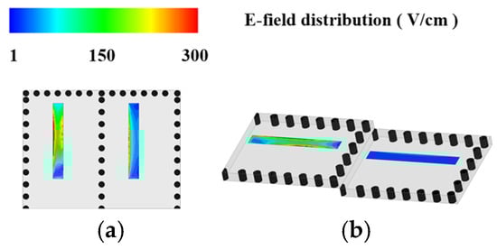
Figure 6.
E-field distributions of (a) latitudinally arranged slot antenna array and (b) ladder-type longitudinally arranged slot antenna array.
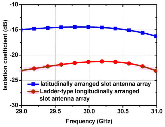
Figure 7.
Simulated coupling coefficients of two types of slot antenna array.
However, this new form of arrangement has raised another problem, as shown in Figure 8. Because the slot antennas are arranged on separate layers, the normal direction has a deviation angle θ0 from the vertical direction, compared with the linear array distributed in the horizontal direction. In other words, the four generated beams would have a rotation angle θ0 from the vertical direction.
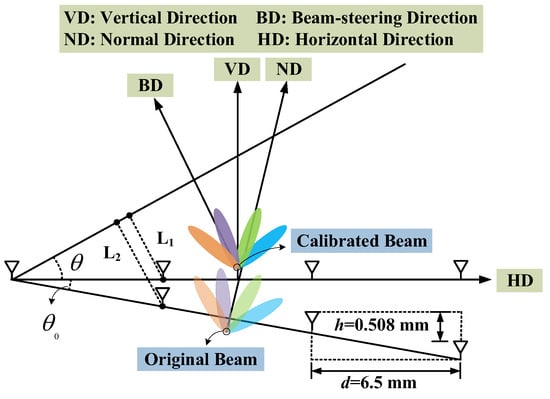
Figure 8.
Calibration theory for beam-steering direction deviation.
To reverse the deviation angle, additional phase shifters should be added to compensate for the wave-path difference. According to Figure 8,
The compensated phase difference can be calculated as
The angle θ0 is a constant, while the beam direction angle θ is a variable depending on the feeding phase differences.
where h is the thickness of Rogers RT/duroid RO5880, d is the distance between adjacent slot antennas, φ is the feeding phase difference in the BM, and λ is the wavelength at the center frequency (30 GHz). By employing the phase differences of ±45° and ±135° produced by a typical 4 × 4 BM, the beam pointing direction angle θ can be calculated as:
Therefore, we take the average :
To calibrate the beam-steering direction of the ladder-type antenna array, four phase shifters are jointed to the four antenna elements separately with the compensatory phase shifting values of , 2, 3, and 4, respectively. This value can be compensated by adjusting the width and length of the SIW path.
4. Multibeam Antenna Design, Fabrication, and Measurement
To further reduce the dimensions and accommodate the ladder-type slot antenna array, some adjustments of the E-plane 4 × 4 BM should be conducted. Figure 9 and Figure 10 show the detailed topology and simulated model of the designed multibeam antenna fed by the modified BM. Firstly, the E-plane 4 × 4 BM is folded to reduce the longitudinal length. Secondly, the compensated phase shifters are embedded into the BM. The phase shifting values are listed in Table 1. The simulated S-parameters and phase differences are plotted in Figure 11. After these adjustments, the original phase differences between adjacent output ports, namely −45°, 135°, −135°, and 45°, are revised to −61°, 119°, −151°, and 29°, respectively. The total architecture covers a remarkably small area of 12 mm × 45 mm × 2 mm (1.2 λ × 4.5 λ × 0.2 λ).
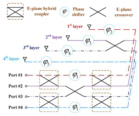
Figure 9.
Block diagram of a four-beam antenna array.
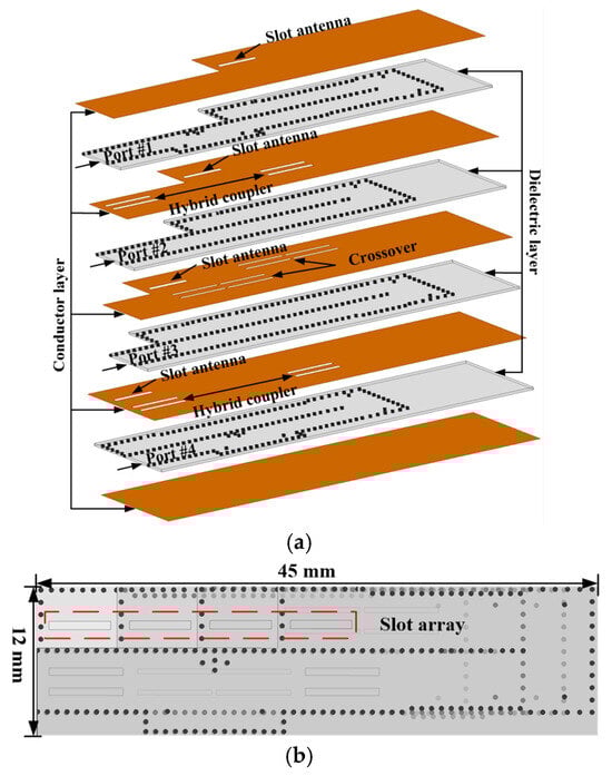
Figure 10.
Simulated model of a four-beam antenna array. (a) Perspective view. (b) Top view.

Table 1.
Phase shifting values (Unit: Degrees).
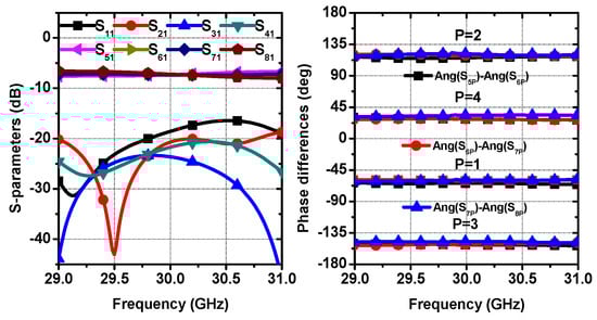
Figure 11.
Simulated S-parameters for port #1 excitation and phase differences in adjusted BM.
4.1. Multibeam Antenna Prototype
Regarding the above-mentioned design details and process, the multibeam antenna fed by the modified BM is manufactured, which contains four Rogers RT/duroid RO5880 laminates. The thickness, loss tangent, and relative dielectric permittivity of the used laminates are 0.508 mm, 0.0009, and 2.2, respectively. As shown in Figure 12, the entire structure is stacked via four separate substrates. It should be noted that some screws are used to fix and tighten separate layers, minimizing air gap thickness. In addition, SIW-to-microstrip transitions are introduced to match the 2.40 mm end launch connectors. The S-parameter measurements are carried out with a Network Analyzer (Agilent E8363B, Agilent Technologies, Santa Clara, CA, USA). The radiation patterns are measured by an NSI far-field measurement system. The array gains are obtained contrastingly to a standard horn antenna.
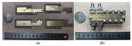
Figure 12.
Photographs of the fabricated four-beam antenna array. (a) Separated layers and (b) assembled prototype.
To evaluate the discrepancy between simulated models and fabricated objects, as depicted in Figure 13, the fabricated thickness of the air gap is calculated based on the measured thicknesses of separate layers and the whole structure. Here, we take multiple measurements and average the testing values to minimize the accidental error. The six calculated values of thickness are 0.04 mm, 0.04 mm, 0.043 mm, 0.037 mm, 0.043 mm, and 0.047 mm, respectively, and they average to be 0.042 mm.
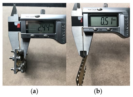
Figure 13.
Measured thicknesses of the (a) multi-layer structure and (b) single-layer substrate.
4.2. Scattering Parameters
The reflection and isolation coefficients for port #1 and port #2 excitations are plotted in Figure 14a and Figure 14b, respectively, including the simulation and measurement cases. The situations for port #3 and port #4 are similar to that of port #1 and port #2 excitations. It can be seen that the reflection and isolation loss are higher than 10 dB from 29 GHz to 31 GHz. The measured and simulated results can be viewed as having acceptable agreement in consideration of the error in fabrication and measurement.
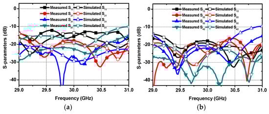
Figure 14.
Simulated and measured S-parameters for (a) port #1 excitation and (b) port #2 excitation.
4.3. Radiation Patterns
Measurements and simulations of the radiation patterns are displayed in Figure 15. For better visualization, the results are normalized. The presented multibeam antenna allows for the achievement of four independent beams pointing in four different directions. By switching the different input ports of the E-plane 4 × 4 BM, one can obtain different directions of the multibeam antenna. When working at 30 GHz, the orientation angles related to four beams are −35°, −13°, 9°, and 32°. Characterized by half-power beam width, the proposed multibeam antenna can provide a scanning range of approximately ±45°.
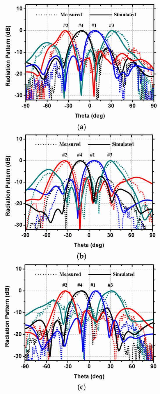
Figure 15.
Measured and simulated radiation patterns of the multibeam antenna array at (a) 29 GHz, (b) 30 GHz, and (c) 31 GHz.
Despite the slight fluctuation of minority beams, it can be observed in Figure 15 that an acceptable agreement between simulated and measured radiation patterns is obtained. In addition to the inevitable air gap mentioned above, fabrication errors and measurement errors can also deteriorate the measured patterns. Radiation patterns at 29 GHz and 31 GHz are also included in Figure 15 to analyze the multibeam characteristics within the operating frequency. A phenomenon that the beam generated by port #3 excitation suffers from relatively high grating lobe level, which rises up to 5 dB, should be paid attention to. After calibration, the original pointing directions (−11°, −35°, 11° and 35°) are revised to be −6°, −30°, 16°, and 40°, taking the linear slot antenna array as reference. According to grating lobe suppression principle,
The spacing of adjacent antenna element d and the pointing direction angel θ have a close relationship with the grating lobe level. The bigger the value of d or |θ| (0° <θ < 90°), the higher grating lobe level appears. After calibration, the biggest pointing angle lies in the beam generated by port #3 excitation. Another factor contributing to the rising grating lobe level is the distance between adjacent antenna elements. In order to not block the radiation of the adjacent antenna element, the distance of the proposed antenna array are determined to be 0.65λ, which do not stick to the regular value of 0.5λ. That is why the simulated and measured radiation patterns both encounter higher grating lobe level.
After addressing the measured data of radiation patterns, the measured gains can be calculated and compared to the simulated results, as shown in Figure 16. Also, the simulated directivity is provided to analyze the BFN loss. In the center frequency of 30 GHz, the simulated gains of the pattern are 11.0 dBi, 10.5 dBi, 9.4 dBi, and 10.6 dBi, respectively, related to port #1 = #4 excitations. Due to the grating lobe level increase, the gain of the beam corresponding to port #3 excitation is lower than that of other port excitations. An acceptable agreement can be viewed between simulated and measured gain. There is a difference of approximately 1 dB between the simulated directivity and gain. As mentioned in Section 2, the insert loss of the BFN is 0.8 dB. Additionally, the SIW to microstrip transition line has brought a 0.2 dB insert loss as well. In other words, the efficiency of the proposed multibeam antenna is approximately 80%.
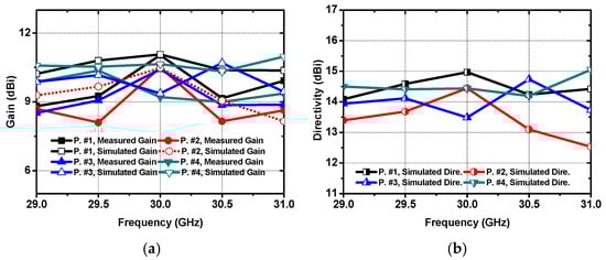
Figure 16.
(a) Simulated and measured gain; (b) simulated directivity.
According to the above analysis, an approximately 1 dB insert loss of the BFN and a relative higher grating lobe level of beam #3 appears. Taking the narrow space for antenna in the terminal device into account, the specification for the terminal device antenna is not as strict as that for other antennas, including S-parameters, efficiency, and so on. For example, when the frequency is lower than 6 GHz, the acceptable return loss level for terminal devise antenna is −6 dB while that for other antennas is −10 dB. Therefore, the performances of the proposed multibeam array antenna may be acceptable for 6G terminal device application.
4.4. Comparison and Discussion
The performance between the proposed multibeam antenna fed by the E-plane BM and other similar designs are summarized in Table 2. For fair comparisons, all these multibeam antennas are based on 4 × 4 BMs and realized in SIW technology. As reported in [11], a traditional multibeam antenna with a single-layer configuration occupies an area of 7.2 × 2.7 λ2. To improve the compactness, a feasible approach is to resort the dual-layer configuration proposed in [12], whose size is 3.0 × 3.0 λ2 without the radiation portion. Utilizing more stacked layers can effectively reduce the footprint, as shown in [17,19,20,21]. It is seen that the multi-layer design in [17] requires an area of 3.3 × 2.9 λ2, which is attributed to the array scale. The designs in [19,20,21] did not straightforwardly include the connection between the 4 × 4 BMs and the radiation portion, thus the radiation performances are omitted here. Facilitating the multibeam antenna design would add an extra area for constructing the connection part. In this work, by using four-layer stacked configuration and ladder-type slot array, a miniaturized multibeam antenna with an area of 4.5 × 1.3 λ2 is achieved. Compared with the single-layer design in [11], the area is reduced by 70%. In contrast to six-layer design in [17], there is a size reduction of 39%. It is seen that the coverage of the proposed multibeam antenna is 67°, which is limited by the spacing between the adjacent antenna elements.
Table 2.
Comparisons Between Multibeam Antennas Fed By 4 × 4 BMs.
5. Conclusions
In this paper, a compact and miniaturized multi-layer multibeam antenna excited by a modified E-plane 4 × 4 BM is proposed. The E-plane 4 × 4 BM is adjusted to eliminate any use of coupling slot and obtain a reduced occupied area. To reduce the mutual coupling effect, an unconventional slot antenna array is adopted. Furthermore, the E-plane 4 × 4 Butler matrix is adjusted for compatibility with the proposed slot antenna array and to achieve further miniaturization. During design, the impacts of the air gap are also taken into consideration to achieve a better agreement between simulated and measured results. The total structure amounts to an area of 12 mm × 45 mm × 2 mm, which is promising for 6G terminal device applications. Theoretical analyses, computer simulations, fabrications, and measurements have been conducted to demonstrate the feasibility of the proposed scheme. As the simulated and measured results vary from 29 GHz to 31 GHz as shown, the reflection and isolation coefficients of the multibeam antenna are less than −10 dB, the measured gains of the multibeam antenna at 30 GHz related to port #1-#4 are 11 dBi, 10.5 dBi, 10.4 dBi, and 9.2 dBi, respectively. The multibeam pattern can provide a scanning range of approximately ± 45°.
Author Contributions
Conceptualization, Q.-Y.W. and J.-W.L.; methodology, J.-W.L.; software, Q.-Y.W., L.-H.W. and C.-Q.B.; investigation, Q.-Y.W., L.-H.W. and C.-Q.B.; writing—original draft preparation, Q.-Y.W.; writing—review and editing, J.-W.L.; supervision, J.-W.L.; project administration, J.-W.L.; funding acquisition, J.-W.L. All authors have read and agreed to the published version of the manuscript.
Funding
This work was supported in part by the National Key Research and Development Program of China under Grant 2024YFE0107800, in part by the National Natural Science Foundation of China under Grant 62101259 and 62025109.
Data Availability Statement
The data that support the findings of this study are available from the corresponding author upon reasonable request.
Conflicts of Interest
The authors declare no conflicts of interest.
Abbreviations
The following abbreviations are used in this manuscript:
| BM | Butler matrix |
| BFN | Beam-forming network |
| SIW | Substrate-Integrated Waveguide |
| MIMO | Massive multi-input multi-output |
| LTCC | Low Temperature Co-fired Ceramic |
References
- Andrew, J.G.; Buzzi, S.; Choi, W.; Hanly, S.V.; Lozano, A.; Soong, A.C.K.; Zhang, J.C. What will 5G be? IEEE J. Sel. Areas Commun. 2014, 32, 1065–1082. [Google Scholar] [CrossRef]
- Rappaport, T.S.; Sun, S.; Mayzus, R.; Zhao, H.; Azar, Y.; Wang, K.; Wong, G.N.; Schulz, J.K.; Samimi, M.; Gutierrez, F. Millimeter wave mobile communications for 5G cellular: It will work! IEEE Access 2013, 1, 335–349. [Google Scholar] [CrossRef]
- Roh, W.; Seol, J.-Y.; Park, J.; Lee, B.; Lee, J.; Kim, Y.; Cho, J.; Cheun, K.; Aryanfar, F. Millimeter-wave beamforming as an enabling technology for 5G cellular communications. IEEE Commun. Mag. 2014, 52, 106–113. [Google Scholar] [CrossRef]
- Staszek, K.; Gruszczynski, S.; Wincza, K. Broadband measurements of broadband Measurements of S-Parameters utilizing 4 × 4 Butler matrices. IEEE Trans. Microw. Theory Tech. 2013, 61, 1692–1699. [Google Scholar] [CrossRef]
- Wincza, K.; Staszek, K.; Slomian, I.; Gruszczynski, S. Scalable multibeam antenna arrays fed by dual-band modified Butler matrices. IEEE Trans. Antennas Propag. 2016, 64, 1287–1297. [Google Scholar] [CrossRef]
- Talbi, A.; Seddiki, M.L.; Ghanem, F. A compact 4 × 4 Butler matrix for UWB applications. In Proceedings of the 2013 IEEE Antennas and Propagation Society International Symposium (APSURSI), Orlando, FL, USA, 7–13 July 2013; pp. 1010–1011. [Google Scholar]
- Ding, K.; He, F.; Ying, X.; Guan, J. A compact 8 × 8 Butler matrix based on double-layer structure. In Proceedings of the 2013 5th IEEE International Symposium on Microwave, Antenna, Propagation and EMC Technologies for Wireless Communications, Chengdu, China, 29–31 October 2013; pp. 650–653. [Google Scholar]
- Li, Y.-L.; Liu, Q.S.; Sun, S.; Gao, S.S. A miniaturized Butler matrix based on patch hybrid couplers with cross slots. In Proceedings of the 2013 IEEE Antennas and Propagation Society International Symposium (APSURSI), Orlando, FL, USA, 7–13 July 2013; pp. 2145–2146. [Google Scholar]
- Tian, G.; Yang, J.-P.; Wu, W. A novel compact Butler matrix without phase shifter. IEEE Microw. Wirel. Compon. Lett. 2013, 24, 306–308. [Google Scholar] [CrossRef]
- Cheng, Y.J. Substrate Integrated Antennas and Arrays; CRC Press: London, UK, 2015; pp. 197–203. [Google Scholar]
- Yang, Q.-L.; Ban, Y.-L.; Kang, K.; Sim, C.-Y.-D.; Wu, G. SIW multibeam array for 5G mobile devices. IEEE Access 2016, 4, 2788–2796. [Google Scholar] [CrossRef]
- Djerefi, T.; Wu, K. A Low-Cost Wideband 77-GHz Planar Butler Matrix in SIW Technology. IEEE Trans. Antennas Propag. 2012, 60, 4949–4954. [Google Scholar] [CrossRef]
- Chen, P.; Hong, W.; Kuai, Z.; Xu, J.; Wang, H.; Chen, J.; Tang, H.; Zhou, J.; Ke, W. A multibeam antenna based on substrate integrated waveguide technology for MIMO wireless communications. IEEE Trans. Antennas Propag. 2009, 57, 1813–1821. [Google Scholar] [CrossRef]
- Li, Y.; Luk, K.-M. A Multi-beam end-fire magneto-electric dipole antenna array for millimeter-wave applications. IEEE Trans. Antennas Propag. 2016, 64, 2894–2904. [Google Scholar] [CrossRef]
- Tekkouk, K.; Hirokawa, J.; Sauleau, R.; Ettorre, M.; Sano, M.; Ando, M. Dual-layer ridged waveguide slot array fed by a Butler matrix with sidelobe control in the 60-GHz band. IEEE Trans. Antennas Propag. 2015, 63, 3857–3867. [Google Scholar] [CrossRef]
- Ali, A.A.M.; Fonseca, N.J.G.; Coccetti, F.; Aubert, H. Design and implementation of two-layer compact wideband Butler matrices in SIW technology for Ku-band applications. IEEE Trans. Antennas Propag. 2010, 59, 503–512. [Google Scholar] [CrossRef]
- Cheng, Y.J.; Bao, X.Y.; Guo, Y.X. 60-GHz LTCC miniaturized substrate integrated multibeam array antenna with multiple polarizations. IEEE Trans. Antennas Propag. 2013, 61, 5958–5967. [Google Scholar] [CrossRef]
- Tekkouk, K.; Ettorre, M.; Coq, L.L.; Sauleau, R. Multibeam SIW slotted waveguide antenna system fed by a compact dual-layer Rotman lens. IEEE Trans. Antennas Propag. 2015, 64, 504–514. [Google Scholar] [CrossRef]
- Yang, W.; Yang, Y.; Che, W.; Fan, C.; Xue, Q. 94-GHz compact 2-D multibeam LTCC antenna based on multifolded SIW beam-forming network. IEEE Trans. Antennas Propag. 2017, 65, 4328–4333. [Google Scholar] [CrossRef]
- Cheng, Y.J.; Bao, X.Y.; Guo, Y.X. Miniaturized multilayer folded substrate integrated waveguide Butler matrix. Prog. Electromagn. 2011, 21, 45–58. [Google Scholar] [CrossRef]
- Lian, J.-W.; Ban, Y.-L.; Yang, Q.-L.; Fu, B.; Yu, Z.-F.; Sun, L.-K. Planar millimeter-wave 2-D beam-scanning multibeam array antenna fed by compact SIW beam-forming network. IEEE Trans. Antennas Propag. 2018, 66, 1299–1310. [Google Scholar] [CrossRef]
- Lian, J.-W.; Ban, Y.-L.; Wu, Y.-Q.; Zhong, L.-H. Miniaturized Multibeam Array Antenna Based on E-Plane Butler Matrix for 5G Application. In Proceedings of the 2018 IEEE International Symposium on Antennas and Propagation & USNC/URSI National Radio Science Meeting, Boston, MA, USA, 8–13 July 2018; pp. 1031–1032. [Google Scholar]
- Xu, X.; Bosisio, R.G.; Wu, K. A new six-port junction based on substrate integrated waveguide technology. IEEE Trans. Microw. Theory Tech. 2005, 53, 2267–2273. [Google Scholar]
- Sellal, K.; Talbi, L.; Denidni, T.A.; Lebel, J. Design and implementation of a substrate integrated waveguide phase shifter. IET Microw. Antennas Propag. 2008, 2, 194–199. [Google Scholar] [CrossRef]
- Liu, B.; Hong, W.; Hao, Z.C.; Wu, K. Substrate integrated waveguide 180-degree narrow-wall directional coupler. In Proceedings of the 2005 Asia-Pacific Microwave Conference Proceedings, Suzhou, China, 4–7 December 2005. [Google Scholar]
- Cheng, Y.J.; Hong, W.; Wu, K. Broadband self-compensating phase shifter combining delay line and equal-length unequal-width phaser. IEEE Trans. Microw. Theory Tech. 2009, 58, 203–210. [Google Scholar] [CrossRef]
- Park, S.-J.; Shin, D.-H.; Park, S.-O. Low side-lobe substrate integrated-waveguide antenna array using broadband unequal feeding network for millimeter-wave handset device. IEEE Trans. Antennas Propag. 2015, 64, 923–932. [Google Scholar] [CrossRef]
- Zhai, G.; Chen, Z.N.; Qing, X. Mutual coupling reduction of compact four-element MIMO slot antennas using metamaterial mushroom structures. In Proceedings of the 2015 International Workshop on Antenna Technology (iWAT), Seoul, Republic of Korea, 4–6 March 2015; pp. 3–6. [Google Scholar]
Disclaimer/Publisher’s Note: The statements, opinions and data contained in all publications are solely those of the individual author(s) and contributor(s) and not of MDPI and/or the editor(s). MDPI and/or the editor(s) disclaim responsibility for any injury to people or property resulting from any ideas, methods, instructions or products referred to in the content. |
© 2025 by the authors. Licensee MDPI, Basel, Switzerland. This article is an open access article distributed under the terms and conditions of the Creative Commons Attribution (CC BY) license (https://creativecommons.org/licenses/by/4.0/).