Abstract
This work presents a novel three-stage low-noise amplifier (LNA) design methodology. The first two stages consist of common-source stages with inductive source degeneration, while the third stage consists of an RC network attached before the common-source FET transistor. The input matching network is designed to meet the optimum noise measurement termination, which results in a noise Figure of less than 1.6 dB. The highest gain level of 25 dB was measured, and the input and output reflection coefficients are better than 10 dB for the operating bandwidth, i.e., 13–15 GHz. The LNA’s large signal performance and robustness against continuous high input power and pulse waves are reported. This LNA can handle up to 15 dBm input pulse of 50 nS width and 10% duty cycle, and 18 dBm continuous wave without noticing an increment in the forward gate current.
1. Introduction
The low-noise amplifier (LNA) is an active semiconductor device widely used in TV broadcasting, satellite communication, and other electronic systems as part of the RF front end [1,2]. It plays a crucial role in the receiving system by enhancing the signal-to-noise ratio (SNR) [3].
When the transistor is properly biased, selecting a low-noise design technique requires balancing the often conflicting goals of minimizing noise, maximizing gain, and achieving input and output impedance matching [4,5]. In conventional low-noise design approaches, selecting a source termination, , does not necessarily result in a simultaneous conjugate match at both the input and output ports of the transistor. Typically, the input is matched for optimal noise performance, while the output is matched for gain. Feedback is often applied to the transistor to adjust the ideal noise match and input impedance, thereby achieving the simultaneous signal and noise match (SSNM) condition. Employing inductive source degeneration techniques in LNA design can further enhance overall efficiency [6,7,8].
A deterministic inductive source degeneration technique was developed to design a two-stage LNA with predetermined gain and a low Noise Figure (NF) [9]. However, in some applications, a two-stage LNA is insufficient to achieve the required amplification gain [10]. Consequently, a third stage is often introduced to increase the gain provided by the preceding stages [11]. While adding more stages to the LNA can enhance performance metrics such as gain and noise Figure under certain conditions, it also introduces several drawbacks, including increased power dissipation [12], higher cost [13], greater design complexity [14], and larger chip area [15]. The deterministic design approach proposed in this work enables a more precise and time-efficient optimization, facilitating a better trade-off among key design parameters.
In our previous work [9], we introduced a straightforward synthesis methodology for a three-stage LNA, building upon the two-stage deterministic technique described in [16]. In that study [9], only the small-signal parameters were characterized. This article presents a comprehensive design methodology for each stage, including a load-pull simulation of the third amplifier stage. The nonlinear performance of the LNA, as well as its robustness under input overdrive conditions for both continuous-wave (CW) and pulsed signals, is also examined.
The LNA MMIC test vehicle, developed using the proposed design approach, was fabricated on 150 mm GaAs wafers employing the WIN Semiconductors PIH1-10 high-integration E-mode pHEMT process with an integrated monolithic PIN diode.
This paper is organized as follows. Section 2 presents the related content in the open literature and highlights the new contributions presented in this article. Section 3 demonstrates the detailed design methodology and the related design figures of merit. The pHEMT MMIC LNA, test bench setups with EM simulations, and measurements are presented in the fourth Section 4. The robustness and reliability of the LNA are discussed in Section 5. Furthermore, Section 6 presents the state-of-the-art LNAs from the open literature along with a figure of merit to distinguish between them. Lastly, a discussion of the work is presented in Section 7.
2. Background
Generally, in a single-stage LNA design, a simultaneous signal and noise match (SSNM) at the input and a conjugate signal match at the output section of the active device cannot be achieved [15]. The designer is responsible for balancing input and output mismatch levels IM and OM, respectively. In either situation, the resulting output or input impedance may have a high reflection coefficient, which is unfavorable to system integration. Impedance matching at the input port will not provide the best noise performance or the lowest input reflection. Therefore, source inductance feedback is introduced to get closer to [17]. By doing this, the impedance matching networks become simpler when and are brought closer to the center of Smith’s chart, as shown in Figure 1.
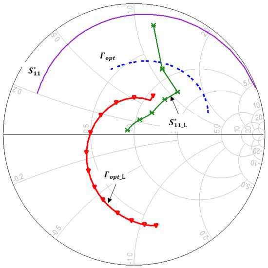
Figure 1.
(purple solid line) and (blue dashed line) of the transistor without inductive feedback. (green-crossed line) and (red diamond line) when inductive feedback is used.
Previously, in [16], the authors introduced the deterministic design technique for the two-stage LNA using the feedback approach, with a linear gain of 18 dB. To obtain a gain of 20–30 dB at microwave frequencies, different LNAs are applied in a three-stage architecture, depending on the technology and the application [18].
In our previous publication [9], we presented a simple synthesis methodology for 3-stage LNA, where only the small signal parameters were presented. This extended and comprehensive contribution will show:
- Comprehensive design details for each stage.
- Noise Figure measurements.
- The LNA’s large-signal performance simulation.
- The LNA robustness under input overdrive for both the continuous-wave (CW) and pulse-wave.
- Comparison with state-of-the-art amplifiers of similar technology.
- Suggestions for improving the proposed amplifier.
3. Proposed Design Methodology
In this part, a detailed design approach will be demonstrated. MATLAB, R2022a, and ADS, 2020, are used in various design steps. The design is generally organized into two main blocks: the two-stage LNA block and the third-stage amplification block, as can be shown in Figure 2.
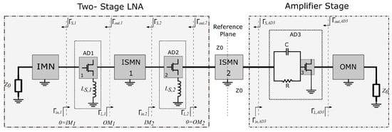
Figure 2.
Three-stage LNA consists of a two-stage LNA followed by an amplifier in the third stage. Reprinted with permission from Ref. [9]. 2025, IEEE.
3.1. Device Selection
The first step in the design process is to select the appropriate transistors from the available technology kit, in this case, the WIN PIH1-10 design kit. Given that two transistor models, 2 × 50 µm and 4 × 75 µm, are available in the design kit, a decision must be made about which should be used in the first, second and last stages. The transistor with the lowest minimum noise figure should be placed in the first stage of the LNA to minimize the overall noise figure, as the noise performance of a cascaded amplifier is dominated by the noise figure of its first stage [10]. A comparison of the minimum noise figures for both models is shown on the left side of Figure 3. It is evident that the µm transistor exhibits a lower noise figure than the µm transistor. Therefore, the former is selected for the first and second stages of the amplifier. On the other hand, the transistor with a gate width of 4 × 75 µm has a higher gain than the 2 × 50 µm FET transistor, right side of Figure 3, consequently, the wider transistor will be placed in the third amplification stage.
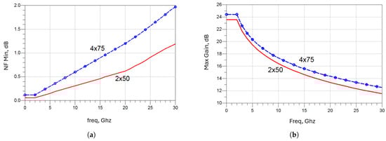
Figure 3.
Performance over frequency for transistor with gate widths: 2 × 50 µm (red solid line) and 4 × 75 µm (blue dashed line): (a) Minimum noise; (b) Maximum gain.
3.2. Two-Stage LNA Design
In this design, a two-stage LNA consists of two similar common-source transistors (2 × 50 µm gate width) connected to the ground through a feedback inductor. A simplified schematic of the two-stage LNA is presented in Figure 4. The FET transistor with its source terminal connected to the ground through an inductor, , will be denoted as the “Active Device” (AD1 and AD2, respectively) in this article.
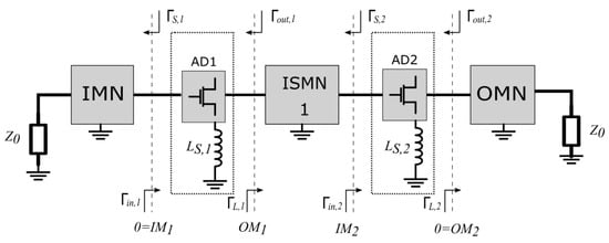
Figure 4.
Two-stage LNA schematic with inductive feedback and matching networks.
The second step in the design is to evaluate the stability of the device to ensure that it operates within its stable region and avoids oscillations during operation. This assessment can be performed by analyzing the input and output stability circles, as illustrated in Figure 5. It is evident that the device is not inherently stable at the design frequency of 15 GHz. Therefore, a stabilization element must be introduced to enhance transistor stability. In this work, a feedback inductor is added to the source terminal of the transistor to ensure stable operation.
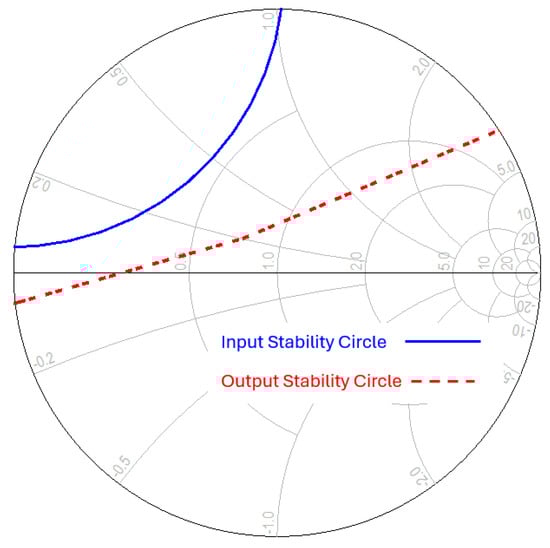
Figure 5.
Input and output stability circles for 2 × 50 µm transistor model.
Other figures of merit of stability are the Rollet stability factor, K, and the stability measure [10]. The necessary and sufficient conditions for unconditional stability are that the stability factor is greater than unity and that the stability measure is positive [15]. Various inductor values are tested to find the minimum value that can stabilize the transistor under the design frequency, and it can be shown from Figure 6, left side, that nH is the minimum inductance value needed to stabilize the transistor at the design frequency. For confirmation, the input and output stability circles with the addition of a nH inductor are also presented to verify that the transistor is unconditionally stable from 13–15 GHz, as shown on the right side of the Figure 6.
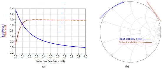
Figure 6.
(a) The active device stability measures vs. inductive feedback values at 15 GHz. (b) The input and output stability circles after the addition of the 0.311 nH feedback inductor to the 2nd stage transistor at 13–15 GHz.
The FET transistors in Figure 4 used in the first and second stages are from the WIN foundry PIH1-10 design kit with a gate width of 2 × 50 µm. Their noise and small signal parameters are reported in Table 1. For simplicity, the same transistor model is used in the first and second stages; however, the method is applicable to be used with different transistor models.

Table 1.
FET small signal and noise parameters with 2 × 50 µm gate width at 15 GHz. The Source terminal is ideally Grounded.
It is important to mention that adding a feedback inductor in series will change the small-signal and noise parameters for the active device. Formulas for determining the small signal and noise values for the active device are accessible in [19].
The input (IMN), output (OMN), and inter-stage (ISMN) matching networks are assumed to be lossless. This assumption has the effect of requiring that each MN’s input and output ports have the same mismatch levels. The reason behind this is that the passive elements in the matching network cannot dissipate or generate power; thus, the incident electrical wave is either reflected or transmitted. and in Figure 4 represent the input and output mismatch levels of the two-stage LNA, respectively. and are the levels of mismatch before and after . means a perfect conjugate match at the input port, implies a purely reactive input reflection coefficient, while indicates a negative resistance [10]. A similar explanation is applied to . The scenario in which and are greater than unity is avoided since it could be detrimental to the RF system.
To meet the SSNM condition, the source termination is selected to meet the optimum termination for noise measurement, [4], the correct equations for calculating the optimum termination can be found in [20]. The input and output reflection coefficients for each stage can be calculated using Equations (1) and (2) [15].
where is the determinant of the matrix of the S parameters of the active device, . The mismatch values at the input and output of each stage can be calculated using Equations (3) and (4), respectively [15]. In all equations, we assume that .
The minimum output mismatch level when the input is matched to (), is known as , while the minimum input mismatch level when the output is matched to (), is defined as [15]. This special scenario can only be met if the input reflection coefficients of the two stages ( and ) are fixed to satisfy the optimum termination of and , respectively.
The third step of the design is to find the exact values of the feedback inductor. To do so, we first determine the minimum level of mismatch in the interstage network. Using the equations available in [11], the vs. and vs. graph is drawn and it is clear from Figure 7 that the minimum value of interstage mismatch is equal to . The reader is free to choose the level of interstage mismatch within the range of . A higher mismatch level will result in a smaller inductance but less stability, Figure 6. In this design, the level of interstage mismatch is set to 0.26, that is, . The corresponding feedback inductor values of these mismatch levels are 0.4 nH and 0.311 nH, to be connected to the first and second stages’ transistors, respectively, as shown in Figure 7.
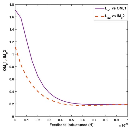
Figure 7.
The first-stage output and second-stage input mismatch levels vs. and , respectively.
The fourth step is to design the IMN, ISMN1, and OMN of the 2-stage LNa, Figure 4. As mentioned earlier, the input matching network is designed to meet the optimum noise measure termination, . The input load is synthesized to satisfy , the latter is the load termination that makes the LNA input perfectly matched to , and its value can be calculated from Equation (5) [15].
where is the determinant of the matrix of the S-parameters of the active device, . The ISMN1 can be designed simply by matching to . On the other hand, the second stage output termination that results in , is simply = . Table 2 summarizes the reflection coefficient values that are required to design the input, interstage, and output matching networks of the two-stage LNA.
Table 2.
Inductance Values, the Corresponding Reflection Coefficients and the Available Gain for the 1st and 2nd Active Devices at 15 GHz for .
The steps for designing the 2-stage LNA can be summarized as follows:
- Select the appropriate device for each stage by comparing the performance of available options.
- Perform stability analyses across the entire operating bandwidth.
- Plot vs. and vs. .
- Draw vs. and vs. .
- Choose the desired interstage mismatch level and determine the corresponding values for and .
- Design the input matching network (IMN), the interstage matching network (ISMN), and the output matching network (OMN).
3.3. Third-Stage Amplifier Design
The minimum gain required for this LNA is 24 dB. It is apparent from Table 2 in the previous section that the total available gain from the first two stages is only dB, which is insufficient to meet the small-signal gain requirement. Therefore, a third amplification stage is necessary. To fulfill this requirement, a gate width transistor of µm from the WIN Foundry PIH1-10 technology is selected for implementation in the third stage. The small-signal and noise parameters of this transistor are provided in Table 3.
Table 3.
FET small signal and noise parameters with 4 × 75 µm gate width at 15 GHz. The source terminal is ideally grounded.
As previously mentioned, once the transistor has been selected, the next step is to evaluate its stability over the operating bandwidth. By plotting the input and output stability circles, it becomes evident that the device is unstable in the frequency range of 13–15 GHz. Therefore, a stabilization network is necessary. Since this stage is treated as a single-stage power amplifier, the stabilization network is introduced at the gate terminal of the transistor rather than its source terminal.
As can be seen in Figure 8, an RC network is inserted before the transistor to improve the bandwidth of the amplifier while increasing the stability of the device. However, the RC network increases the noise Figure for the third stage, but this will not affect the overall LNA’s NF. According to [10], if the gain is high enough, the first stage amplifier will dominate the noise characteristic of cascaded amplifiers. The preliminary values of the resistor and capacitor in the RC network are chosen to make Rollett’s stability factor of the active device higher than unity and achieve a minimum available gain of 7 dB.
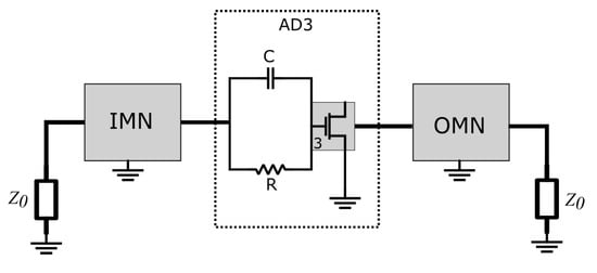
Figure 8.
The Third Stage Amplification Block.
The RC network and the FET can be considered as a single active device, denoted as ‘AD3’, as illustrated in Figure 8. A load-pull simulation, shown in Figure 9, is conducted to determine the source and load impedance values that yield the highest available power gain [10]. The corresponding input impedance, , and output impedance, , are listed in Table 4. To design the IMN and OMN for the final stage, the input and output impedances are matched to the system reference impedance, .
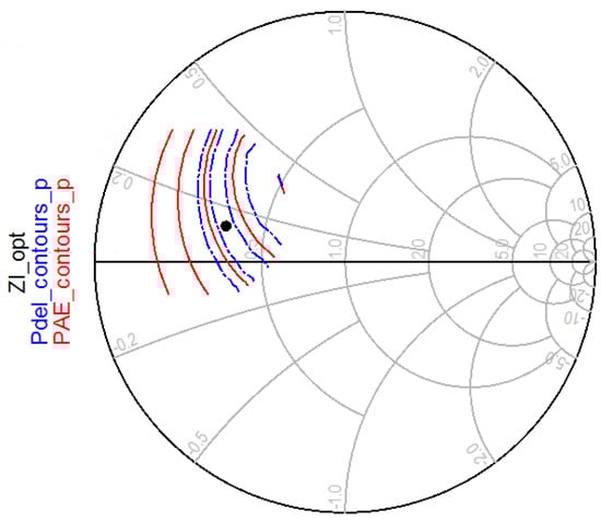
Figure 9.
Load-pull simulation for the Amplifier Stage; power delivered to the load (blue), power added efficiency (red), and the optimum output load (black dot).
Table 4.
Source and Load Termination for the Third Stage Amplifier.
To summarize the design steps of the third stage, the reader can follow these steps:
- Determine the appropriate transistor device.
- Perform a stability analysis and insert a stabilization network at the gate terminal if necessary.
- Perform a load-pull simulation to determine the optimum load impedance that maximizes power gain delivered to the load.
- Match the input and output impedances to the system reference impedance to design the IMN and OMN of the final stage.
3.4. Biasing Networks and Optimization
The schematic of the ideal three-stage amplifier, including the input, output, and interstage networks, is shown in Figure 10.
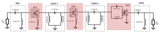
Figure 10.
The 3-stage LNA schematic with the ideal components.
The next step in the design is to implement the biasing networks required to supply the transistors. A DC feed inductor and a DC block capacitor are inserted for each gate and drain terminal. These components are integrated into the IMN, ISMN1, ISMN2, and OMN of the three-stage LNA. The ideal components are then replaced with their counterparts in the WIN PIH1-10 PDK. This step is essential, as the physical models account for inductive effects and losses across different layers [21]. An optimization process is then performed to restore the circuit to meet the original design specifications.
To enhance the robustness of the device, the gate and drain bias lines are fed through resistors [22]. These resistors help protect the device against input overdrive and, according to simulations, do not negatively affect small-signal or noise performance. Figure 11 shows the complete schematic containing the biasing networks and the 3-stage LNA, which was introduced in Figure 10.
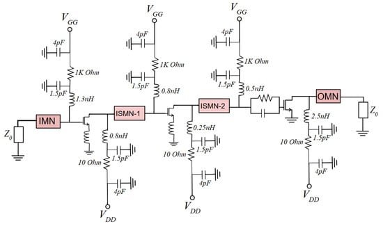
Figure 11.
The complete schematic containing the biasing networks and the 3-stage LNA, which was introduced in Figure 10.
Finally, a layout is generated for fabrication. Figure 12 shows the final MMIC realization of the three-stage LNA.
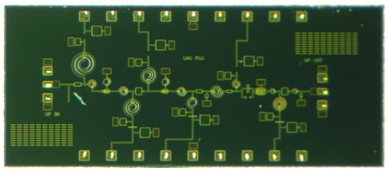
Figure 12.
Realized 3.0 mm × 1.4 mm MMIC of the Three-Stage LNA using WIN PIH1-10 GaAs Technology. Reprinted with permission from Ref. [9]. 2025, IEEE.
4. LNA Characterization
The LNA presented in Figure 12 has chip dimensions of (3.0 mm × 1.4 mm) including PADs. The transistors of the first and second stages have similar biasing at: V and V. The third stage transistor is biased using V and V. Hence, the total DC power dissipated by this device is 362 mW. The bias voltages and currents of each stage were chosen to meet the design requirements of gain, noise figure, and bandwidth. However, this choice led to a higher DC power dissipation; it is less than the maximum DC power consumption allowed of 0.5 W, which was set in the design requirements.
4.1. Measurement Setups
On the wafers, the parameters S were measured using Hewlett-Packard HP8510C Vector Network Analyzer (VNA) in the 10–20 GHz frequency range with increments of 100 MHz. To ensure linear operation of the device under test (DUT), the source power was set to −8 dBm, and a 10 dB internal attenuation was applied at port 1. RF and DC access to the MMIC was provided using a M150 microwave probe station, from CASCADE MicroTech, along with probes from GGB Industries. The system calibration was carried out using Short-Open-Load-Through (SOLT) calibration substrate (CS5) provided by GGB Industries. The complete setup for this test bench is available on the left side of Figure 13.
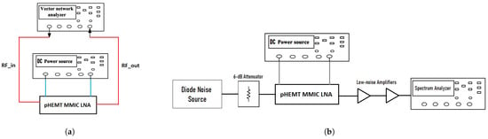
Figure 13.
Test bench setups for the small signal and noise figure measurements from 10–20 GHz: (a) S-parameters test bench and (b) Noise figure test bench.
The noise figure was measured using an Agilent E4448A Power Spectrum Analyzer, which was preceded by two low-noise amplifiers (MACOM MAAM-011109 and Hewlett-Packard HP83051A) for preamplification. A standard Y-factor setup was used, incorporating a diode noise source (Noise Com NC346KA) along with a well-matched 6 dB attenuator. The complete test bench setup is shown on the right side of Figure 13. In both test setups, measurements were automatically collected by a PC running LabVIEW, with communication to the instruments established via a LAN connection.
Nonlinear measurements were performed with an Agilent E4448A Power Spectrum Analyzer, coupled with an absolute power reference provided by Keysight USB power sensor. The test bench setup schematic for power measurements can be seen in Figure 14, while the real measurement setup from our laboratory is available in Figure 15.
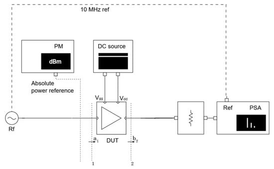
Figure 14.
Test bench setup used for large signal measurements.
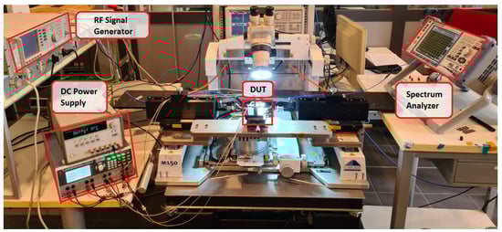
Figure 15.
A picture of the large signal measurements test bench taken in the laboratory used for.
4.2. EM Simulations and Measurements
The small signal and noise measurements agree well with the simulations, as can be depicted in Figure 16. The input and output return losses are better than −10.8 dB and −12 dB, respectively. The peak gain of 25 dB is registered at 13 GHz, and the maximum measured NF is 1.6 dB. Any discrepancy between the simulations and the measurements originates from the measurement test bench.
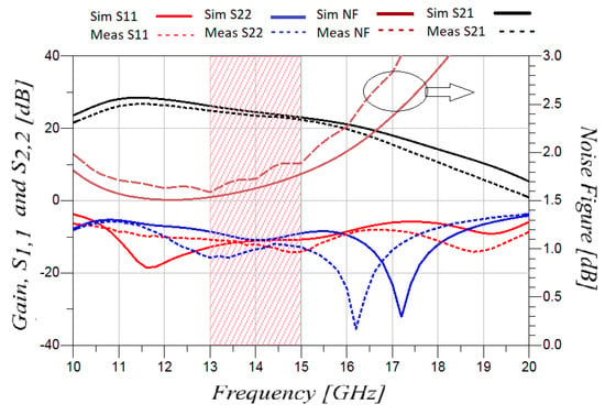
Figure 16.
Measured and EM simulated gain, input and output matching, and noise figure for the pHEMT MMIC LNA.
The EM simulated power and gain response of the designed LNA can be found in Figure 17, while the measured power and gain are illustrated in Figure 18. The input vs. output power levels from the measurements are in good agreement with the EM simulations. The discrepancy between the simulations and the measurements originates from the measurement test bench. Finally, the resulting Power Added Efficiency, PAE, is plotted in Figure 19. From the power measurements, Figure 18a, the pairs are (−9, 17) dBm at 13 GHz, (−8, 16.8) dBm at 14 GHz and (−7.5, 16.2) dBm at 15 GHz.
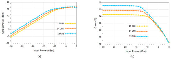
Figure 17.
The nonlinear EM simulated response of the three-stage LNA at 13, 14, and 15 GHz. (a) Output power (dBm) and (b) Gain (dBm).
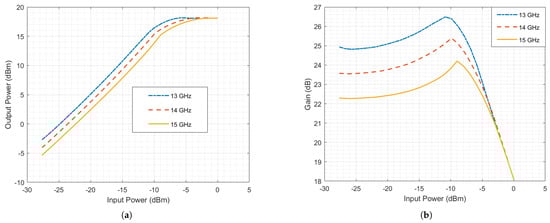
Figure 18.
The nonlinear measured response of the three-stage LNA at 13, 14, and 15 GHz. (a) Output power (dBm) and (b) Gain (dB).
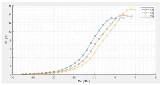
Figure 19.
The resulting Power Added Efficiency, PAE, at 13, 14, and 15 GHz.
5. LNA Robustness
LNA robustness refers to the ability of a Low Noise Amplifier (LNA) to maintain reliable performance under stressful conditions, particularly when subjected to high input power levels and electromagnetic interference (EMI) [23]. Verification of LNA robustness ensures that the amplifier can withstand harsh or unexpected RF environments without degrading performance or damaging the system. It is especially critical in high-reliability, high-power RF applications.
The LNA’s robustness to overdrive continuous wave (CW) and pulse wave input power can be assessed by analyzing its forward gain behavior [22]. To do this, an EM simulation is carried out to predict the forward gate current response when the LNA is subject to high CW power, Figure 20. Under input overdrive conditions, the forward gate current begins to increase, which will result in performance degradation. For safe operation, the forward gate current should not exceed 0.2 mA per finger, as recommended by the manufacturer. According to simulations in Figure 20, the maximum input power that the amplifier can tolerate before performance degradation is observed is 18 dBm at 13 GHz and 19 dBm at 15 GHz.
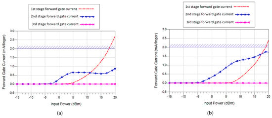
Figure 20.
Forward gate currents vs. different CW input power levels: (a) at 13 GHz, (b) at 15 GHz.
Radio transceiver systems are highly susceptible to electromagnetic interference (EMI), including high-intensity radiated fields, lightning strikes, and high-power microwaves [23]. Electromagnetic pulses (EMPs) can lead to temporary malfunctions or permanent damage to internal electronics and circuitry.
To simulate the LNA’s response under exposure to high-intensity EMPs, various impulse waveforms were injected into its gate terminal. A sinusoidal signal modulated by a square pulse was used to emulate a typical EMP waveform, as illustrated in Figure 21. The pulse power was gradually increased from 5 dBm to 15 dBm, with a fixed pulse width of 50 ns and varying duty cycles of 10%, 15%, and 20%.
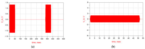
Figure 21.
The square pulse-modulated sinusoidal signal of 50 nSec and 15% duty cycle at 15 GHz frequency and 10 dBm pulse power: (a) The input pulse, (b) Zoom of the input pulse.
When such a pulse is applied, the output becomes non-uniform and varies over time. Therefore, the calculation of the root mean square (r.m.s), as given by Equation (6) [10], is necessary to evaluate the resulting current, voltage, and power values.
Here, T represents the duration of the injected pulse, and denotes the forward gate current as a function of time. The maximum forward gate current recommended for safe operation using this technology is 2 mA per finger. Therefore, the LNA operates within its safe region as long as the gate currents in all stages—, , and —do not exceed this limit.
Table 5 summarizes the pulse values that will result in safe operation of the LNA, according to the simulation results.
Table 5.
Pulse values that will result in the safe operation of the LNA.
6. State of the Art and Figure of Merit
A comparison between previous low-noise amplifiers available in open sources can be found in Table 6. The proposed LNA offers the highest available gain among others while meeting an NF of less than 1.6 dB over the entire two-GHz bandwidth, i.e., 13–15 GHz. The area-aware Figure of Merit (), Equation (7) [24], is calculated to provide a comparative indicator of performance across different LNAs reported in the open literature using similar technology and operating frequency ranges.
where is the bandwidth in GHz, is the gain of the LNA on the linear scale, F is the noise measure, which can be found from the expression , is the total dissipated power in mW and A is the area of the realized LNA in mm2. According to this FoM, the LNA proposed in this manuscript has the highest area-aware FoM at 0.933, making it the best performer in terms of balancing bandwidth, gain, noise, power, and area.
Table 6.
Comparison of the proposed amplifier with previously published Ku-band low-noise amplifier GaAs MMICs.
The proposed LNA can withstand continuous-wave (CW) input powers of up to 18 dBm and pulse-wave inputs of up to 15 dBm before performance degradation occurs. To the best of our knowledge, this is the only GaAs-based LNA design reported to demonstrate robustness under input power overdrive conditions for CW and pulsed signals in the open literature.
7. Discussion
A novel deterministic design methodology is introduced to enhance the performance of a two-stage low-noise amplifier (LNA). The primary objective is to develop a three-stage LNA that achieves the lowest possible noise figure and the maximum available gain, while ensuring proper input and output impedance matching to the reference impedance. The first and second stages utilize a deterministic design based on inductive feedback, whereas the third stage is designed using load-pull simulations to optimize the input and load impedances for maximum output power and gain. Small-signal and noise measurements were conducted, along with electromagnetic (EM) simulations under continuous-wave (CW) and pulsed excitations, to evaluate the reliability and robustness of the LNA when exposed to high-intensity electromagnetic pulses.
The bias voltages and currents of the transistors were carefully selected to ensure optimal performance in terms of gain, noise figure, and bandwidth. Specifically, the biasing points were chosen to strike an effective balance between achieving a low noise figure and maintaining adequate power gain. However, we recognize that power consumption remains a critical consideration in modern circuit design, particularly for energy-efficient systems, as highlighted in Table 6. To reduce power consumption, several strategies can be considered, including:
- Optimize the biasing points to minimize the total current while maintaining performance. This could involve fine-tuning the VGS and VDS values based on a more detailed optimization process, considering the specific trade-offs for noise, gain, and power efficiency.
- Exploring the use of lower power transistors or alternative technologies that offer similar performance with reduced power requirements.
These techniques can help reduce power consumption without sacrificing performance, and we will consider them in future iterations of the design.
Author Contributions
Conceptualization, F.A. and P.E.L.; methodology, F.A.; software, F.A.; validation, F.A., P.E.L. and E.L.; formal analysis, F.A. and P.E.L.; investigation, W.C., S.C. and A.S.; measurements, W.C., S.C. and A.S.; resources, P.E.L.; writing—original draft preparation, F.A.; writing—review and editing, P.E.L.; supervision, E.L.; project administration, E.L.; funding acquisition, P.E.L. and E.L. All authors have read and agreed to the published version of the manuscript.
Funding
This research received no external funding.
Data Availability Statement
Data are contained within the article.
Acknowledgments
The authors thank David Danzilio and the Customer Engineering Department at WIN Semiconductors Corp. for granting access to technology within the Mm Wave for Select Universities program for the Microwave Engineering Center for Space Applications (MECSA). They would also like to thank Filippo Bolli and Enzo De Angelis for their support in characterizing the low-noise amplifier.
Conflicts of Interest
The authors declare no conflicts of interest. This paper reflects the views of the scientist and not those of the company or institute.
Abbreviations
The following abbreviations are used in this manuscript:
| pHEMT | Pseudomorphic High Electron Mobility Transistor |
| MMIC | Monolithic Microwave Integrated Circuit |
| FET | Field Effect Transistor |
References
- Brauer, F.; Sabath, F.; ter Haseborg, J.L. Susceptibility of IT Network Systems to Interferences by HPEM. In Proceedings of the 2009 IEEE International Symposium on Electromagnetic Compatibility, Austin, TX, USA, 17–21 August 2009; pp. 237–242. [Google Scholar]
- Radasky, W.A.; Baum, C.E.; Wik, M.W. Introduction to the special issue on high-power electromagnetics (HPEM) and intentional electromagnetic interference (IEMI). IEEE Trans. Electromagn. Compat. 2004, 46, 314–321. [Google Scholar] [CrossRef]
- Gold, S.; Nusinovich, G.S. Review of high-power microwave source research. Rev. Sci. Instruments 1997, 68, 3945–3974. [Google Scholar] [CrossRef]
- Haus, H.A.; Adler, R.B.; Teichmann, T. Circuit Theory of Linear Noisy Networks; John Wiley & Sons, Inc.: New York, NY, USA, 1959. [Google Scholar]
- Fukui, H. Available Power Gain, Noise Figure, and Noise Measure of Two-Ports and Their Graphical Representations. IEEE Trans. Circuit Theory 1966, 13, 137–142. [Google Scholar] [CrossRef]
- Iversen, S. The effect of feedback on noise figure. Proc. IEEE 1975, 63, 540–542. [Google Scholar] [CrossRef]
- Engberg, J. Simultaneous Input Power Match and Noise Optimization Using Feedback. In Proceedings of the 1974 4th European Microwave Conference, Montreux, Switzerland, 10–13 September 1974; pp. 385–389. [Google Scholar] [CrossRef]
- Vendelin, G. Feedback Effects on the Noise Performance of GaAs MESFETs. In Proceedings of the 1975 IEEE-MTT-S International Microwave Symposium, Palo Alto, CA, USA, 12–14 May 1975; pp. 324–326. [Google Scholar] [CrossRef]
- Abdalrahman, F.; Longhi, P.E.; Limiti, E. A Simple Synthesis Methodology for 3-Stage LNA Design in GaAs Technology. In Proceedings of the 2024 19th Conference on Ph.D. Research in Microelectronics and Electronics (PRIME), Larnaca, Cyprus, 9–12 June 2024; pp. 1–4. [Google Scholar] [CrossRef]
- Pozar, D.M. Microwave engineering. IEEE Potentials 1989, 8, 11–13. [Google Scholar]
- Abdalrahman, F.; Longhi, P.E.; Colangeli, S.; Ciccognani, W.; Serino, A.; Limiti, E. Insight into Optimally Noise- and Signal-Matched Three-Stage LNAs and Effect of Inter-Stage Mismatch. Electronics 2025, 14, 1967. [Google Scholar] [CrossRef]
- Lee, T. The Design of CMOS Radio-Frequency Integrated Circuits, 2nd ed.; Cambridge University Press: New York, NY, USA, 2004. [Google Scholar]
- Razavi, B. RF Microelectronics, 2nd ed.; Communications Engineering and Emerging Technologies Series; Prentice Hall: Hoboken, NJ, USA, 2011. [Google Scholar]
- Friis, H.T. Noise Figures of Radio Receivers. Proc. IRE 1944, 32, 419–422. [Google Scholar] [CrossRef]
- Gonzalez, G. Microwave Transistor Amplifiers: Analysis and Design, 2nd ed.; Prentice-Hall, Inc.: Hoboken, NJ, USA, 1996. [Google Scholar]
- Salvucci, A.; Longhi, P.E.; Colangeli, S.; Ciccognani, W.; Serino, A.; Limiti, E. A straightforward design technique for narrowband multi-stage low-noise amplifiers with I/O conjugate match. Int. J. Microw. Comput.-Aided Eng. 2019, 29, e21833. [Google Scholar] [CrossRef]
- Jiang, N.; Garcia, D.; Niranjanan, P.; Halman, M.A.; Wevers, I. Extremely Low Noise UHF-Band Amplifiers for Square Kilometer Array. In Proceedings of the SPIE Astronomical Telescopes + Instrumentation Conference, Edinburgh, UK, 26 June–1 July 2016. [Google Scholar]
- Fung, A.; Samoska, L.; Bowen, J.; Montanez, S.; Kooi, J.; Soriano, M.; Jacobs, C.; Manthena, R.; Hoppe, D.; Akgiray, A.; et al. X- to Ka-Band Cryogenic LNA Module for Very Long Baseline Interferometry. In Proceedings of the 2020 IEEE/MTT-S International Microwave Symposium (IMS), Los Angeles, CA, USA, 4–6 August 2020; pp. 189–192. [Google Scholar] [CrossRef]
- Engberg, J.; Larsen, T. Noise Theory of Linear and Nonlinear Circuits; Wiley: Hoboken, NJ, USA, 1995. [Google Scholar]
- Poole, C.; Grammenos, R. Correct Equations for Minimum Noise Measure of a Microwave Transistor Amplifier. IEEE Trans. Microw. Theory Tech. 2022, 70, 1361–1366. [Google Scholar] [CrossRef]
- Colantonio, P.; Giannini, F.; Limiti, E. Power Amplifier Fundamentals. In High Efficiency RF and Microwave Solid State Power Amplifiers; John Wiley Sons, Ltd.: Hoboken, NJ, USA, 2009; Chapter 1; pp. 1–47. [Google Scholar] [CrossRef]
- Rudolph, M.; Dewitz, M.; Liero, A.; Khalil, I.; Chaturvedi, N.; Wipf, C.C.; Bertenburg, R.; Miller, J.; Wurfl, J.; Heinrich, W.; et al. Highly Robust X-Band LNA with Extremely Short Recovery Time. In Proceedings of the 2009 IEEE MTT-S International Microwave Symposium Digest, Boston, MA, USA, 7–12 June 2009; pp. 781–784. [Google Scholar]
- Klunder, C.; ter Haseborg, J.L. Effects of High-Power and Transient Disturbances on Wireless Communication Systems Operating Inside the 2.4 GHz ISM Band. In Proceedings of the 2010 IEEE International Symposium on Electromagnetic Compatibility, Fort Lauderdale, FL, USA, 25–30 July 2010; pp. 359–363. [Google Scholar]
- Song, I.; Jeon, J.; Jhon, H.S.; Kim, J.; Park, B.G.; Lee, J.D.; Shin, H. A Simple Figure of Merit of RF MOSFET for Low-Noise Amplifier Design. IEEE Electron. Device Lett. 2008, 29, 1380–1382. [Google Scholar] [CrossRef]
- Dong, Q.; Liang, C.; Tan, Y.; Gao, Z.; Zhao, Y.; Dong, X.; Liu, Y.; Tang, B.; Guo, Z.; Xue, Z.; et al. A Ku-Band TRX Front-End with High Performance in 0.15-μm GaAs PHEMT Technology. In Proceedings of the 2024 IEEE International Symposium on Radio-Frequency Integration Technology (RFIT), Chengdu, China, 28–30 August 2024; pp. 1–3. [Google Scholar] [CrossRef]
- Arican, G.O.; Akcam, N.; Yazgan, E. Ku-Band MMIC LNA Design for Space Applications. In Proceedings of the 2019 6th International Conference on Electrical and Electronics Engineering (ICEEE), Istanbul, Turkey, 16–17 April 2019; pp. 274–278. [Google Scholar] [CrossRef]
- Li, Y.; Mou, S. A Ku-Band Self-Biased Bidirectional Amplifier in 0.25 μm PHEMT Technology. In Proceedings of the 2020 IEEE 6th International Conference on Computer and Communications (ICCC), Chengdu, China, 11–14 December 2020; pp. 1166–1170. [Google Scholar] [CrossRef]
- Rajdev, N.C.; Lasya, V.; Seethur, R. Design of dual-stage Ku-band low noise amplifier for satellite downlink application. EPSTEM 2022, 21, 196–201. [Google Scholar] [CrossRef]
Disclaimer/Publisher’s Note: The statements, opinions and data contained in all publications are solely those of the individual author(s) and contributor(s) and not of MDPI and/or the editor(s). MDPI and/or the editor(s) disclaim responsibility for any injury to people or property resulting from any ideas, methods, instructions or products referred to in the content. |
© 2025 by the authors. Licensee MDPI, Basel, Switzerland. This article is an open access article distributed under the terms and conditions of the Creative Commons Attribution (CC BY) license (https://creativecommons.org/licenses/by/4.0/).