Abstract
TID effects occur in MOS-gated transistors in radiation environments where proton and gamma-rays irradiate the devices. TID effects seriously affect the electrical characteristics of Metal-Oxide-Semiconductor Field-Effect Transistor (MOSFET). They can eventually result in the malfunction of power systems when exposed to long-term radiation conditions. We irradiated gamma-rays and protons into 1.2 kV SiC MOSFETs and evaluated the change in electrical properties to analyze the TID’s effects. As a result of the experiment, the threshold voltage (VT) and on-resistance (Ron) of 1.2 kV SiC MOSFETs decreased because positive fixed charges inside the oxide increased depending on the radiation dose of the gamma-ray and fluence of the proton irradiations. The degradation of breakdown voltage (BV) occurred owing to a change in the depletion curvature at the edge of termination regions owing to the trapping of the charge in the field’s oxide.
1. Introduction
Silicon carbide (SiC) metal-oxide-semiconductor field-effect transistors (MOSFETs) have garnered attention in the field of power electronics, particularly for their high-voltage applications and utilization in radiation environments [1,2]. SiC MOSFETs have various merits, such as low on-resistance, small gate charge, outstanding dv/dt capability, and high-temperature reliability owing to their wide bandgap properties.
However, when the MOSFET is exposed to radiation, positive fixed charges in the oxide increase owing to the effects of the total ionizing dose (TID) [3,4]. The TID affects the change in electrical characteristics, such as the threshold voltage (VT) and on-resistance (Ron). In addition, the curvature of the depletion region becomes narrow due to positive fixed charges generated in the thick field oxide layer of the edge termination region. As the electric field is concentrated in this region, the blocking characteristics deteriorate after exposure to radiation. Furthermore, radiation-induced damage leads to the formation of interfacial defects, resulting in a reduction in channel mobility and an increase in the leakage current [5].
Radiation poses a significant challenge to the reliability of power systems [6,7,8]. Given that radiation exists both in the atmosphere and the space environment, it is imperative to account for its effects in aerospace applications [9,10,11,12]. Several research groups reported numerous investigations into the radiation effects on Si MOSFETs [13,14,15,16,17,18,19,20]. In this study, the SiC MOSFETs were irradiated with gamma-rays and protons to analyze the radiation effects by evaluating VT, Ron, and breakdown voltage (BV). In addition, the TID’s effects were investigated by analyzing the capacitance–voltage (C-V) characteristics of the n-type SiC MOS capacitors to extract the fixed charge density (QF) inside the oxide. Additionally, degradation mechanisms of SiC MOSFETs were elucidated through the Sentaurus TCAD simulations.
2. Experimental Details
In this study, we employed 1.2 kV/189 of mΩ n-channel SiC MOSFETs and n-type SiC MOS capacitors. Figure 1 shows the cross-sectional views of the conventional SiC MOSFET power devices. The studied devices are commercial SiC MOSFETs from STMicroelectronics. The rated voltage of the devices was 1200 V. The SiC MOSFETs and MOS capacitor TEGs were irradiated by a gamma radiation source of 1.33 MeV of Co-60 gamma-rays at the Advanced Radiation Technology Institute (ARTI) in Korea.
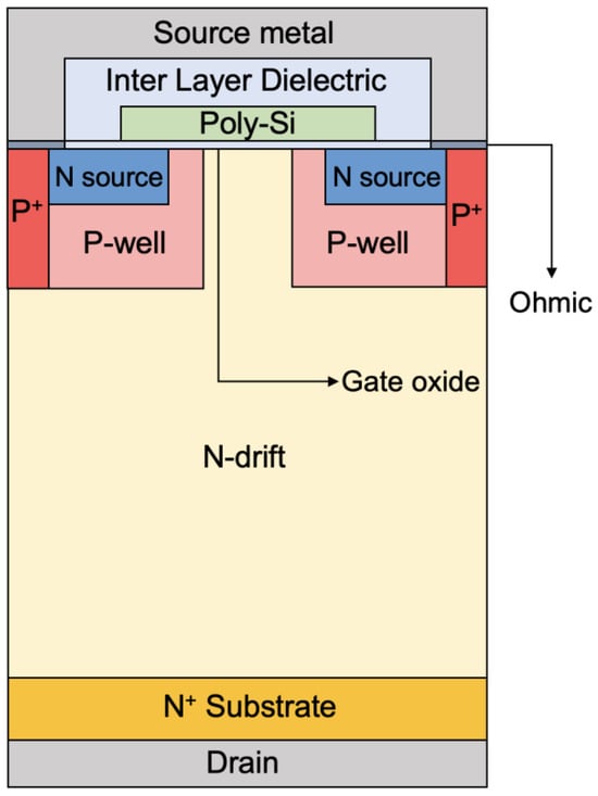
Figure 1.
A cross-sectional view of a conventional SiC MOSFET.
The SiC MOSFETs and n-type MOS capacitors were irradiated using a gamma radiation source of 1.33 MeV of Co-60 gamma-rays at the Advanced Radiation Technology Institute (ARTI) in Korea. Each device was irradiated with the gamma-ray doses of 1, 3, and 5 Mrad for each device. In addition, we irradiated 1.2 kV MOSFETs and n-type MOS capacitors with protons containing 45 MeV of energy with a fluence of 1 × 1012 cm−2 and 1 × 1013 cm−2, respectively, at the Korea Multi-Purpose Accelerator Complex (KOMAC). Specific irradiation conditions in this experiment are summarized in Table 1.

Table 1.
Type and conditions of radiation in the experiment.
We analyzed the electrical characteristics of SiC MOSFETs by analyzing their current–voltage (I–V) characteristics before and after gamma irradiation. Additionally, we analyzed n-type SiC MOS capacitors to verify the TID effect caused by gamma irradiation. We fabricated an N-type MOS capacitor and used it in our experiments to extract the capacitance per unit area of the oxide to accurately analyze the fixed charge inside the oxide. The C-V characteristics of n-type SiC MOS capacitors were analyzed to evaluate the oxide characteristics caused by irradiation. Commercial SiC MOSFETs were measured with Keysight’s B1505A (Santa Rosa, CA, USA) (power device analyzer), and n-type SiC MOS capacitors were measured with Keysight’s B1500A (semiconductor device parametric analyzer).
3. Experimental Results
In Figure 2, the transfer characteristics of 1.2 kV of SiC MOSFETs before and after gamma-ray irradiation are depicted. The irradiated samples exhibit a higher drain current in both sub-threshold and saturation regions, which can be attributed to a reduction from the VT. The extracted ΔVT (=VT,before − VT,after) for various irradiation conditions are 0.498 V (sample 1), 0.697 V (sample 2), and 0.797 V (sample 3). Hole traps were created inside the oxide because of the TID effects caused by gamma irradiation. The increase in QF affects the charge distribution at the SiC regions near the interface and causes more electrons to accumulate in the JFET region, reducing the VT.

Figure 2.
Measured transfer I–V curves (VGS–ID) of 1.2 kV SiC MOSFETs after gamma-ray irradiation.
Figure 3 shows the breakdown characteristics of 1.2 kV SiC MOSFETs before and after gamma-ray irradiation. The BV decrease depends on the gamma-ray irradiation dose. Consequently, the BV decreased by 58 V (sample 1), 64 V (sample 2), and 71 V (sample 3). This was due to the creation of hole traps in the thick oxide at the edge of the termination region, which reduces the curvature of the depletion region. The electric field is concentrated in the depletion region with a small curvature, causing the breakdown characteristics to deteriorate. Since SiC MOSFETs are designed with better breakdown characteristics in the edge termination region than in the active region, the degradation of breakdown characteristics has a fatal effect on electrical characteristics. The mechanism of breakdown degradation is discussed in detail through the simulation results.

Figure 3.
Measured breakdown characteristics (VDS–ID) of 1.2 kV SiC MOSFETs after gamma-ray irradiation.
Figure 4 shows the transfer characteristics of 1.2 kV SiC MOSFETs before and after the proton irradiation. As the proton irradiation fluence (φproton) increased, the VT decreased so that samples 4 and 5 had ΔVT of 0.398 V and 0.776 V, respectively. The VT decreases induced by the hole traps were created due to the TID effects caused by high-energy proton irradiation. Decreasing VT results in unintended turn-on, increased leakage current, and degraded breakdown characteristics, which could lead to power loss or reduced reliability.

Figure 4.
Measured transfer I–V curves (VGS–ID) of 1.2 kV SiC MOSFETs after 45 MeV proton irradiation.
As shown in Figure 5, the BV for samples 4 and 5 are decreased by 30 V and 44 V, respectively. The TID effects lead to the creation of hole traps within the thick oxide layer at the edge termination region. This causes a decrease in surface depletion, which leads to an increase in the surface electric field, consequently diminishing the BV.
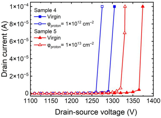
Figure 5.
Measured breakdown characteristics (VDS–ID) of 1.2 kV SiC MOSFETs after 45 MeV proton irradiation.
Our experimental results show that both gamma-ray and proton irradiation result in the degradation of blocking capability with an increased leakage current. The comparative data for the electric characteristics of the SiC MOSFETs before and after gamma-ray or proton irradiation are summarized in Table 2.
Table 2.
Summary of electrical characteristics of 1.2 kV SiC MOSFETs according to the dose of gamma-ray and proton fluences.
When gamma-rays and protons irradiate the MOS structure, electron-hole pairs (EHPs) are produced within the oxide owing to the high-energy radiation by TID effects. Subsequently, holes tend to remain within the oxide layer, primarily due to the relatively higher carrier mobility of electrons compared to that of holes, as discussed in [21,22]. The presence of holes has a notable impact on the charge distribution at the surface of SiC, influencing VT [23,24,25]. Additionally, more electrons are accumulated in the JFET regions, leading to a reduction in on-resistance SiC MOSFETs [26]. Furthermore, the hole traps generated within thick field oxide at the edge of the termination regions induced by TID effects influence a reduction in the surface depletion and the concentration of the electric field at the surface, causing a decrease in BV [27]. We fabricated n-type MOS capacitors to investigate the effects of gamma-ray and proton irradiation on the oxide layer. We used a 10 µm thick drift layer with a doping concentration of 1.1 × 1016 cm–3. Dry oxidation was performed at 1350 °C to form a 50 nm thick gate oxide, followed by NO annealing at 1250 °C. Subsequently, 4 µm thick Al was patterned as a pad metal. The fabricated n-type MOS capacitors were subjected to gamma-ray irradiation at doses of 1, 3, and 5 Mrad, as well as proton irradiation at fluences of 1 × 1012 cm−2 and 1 × 1013 cm−2.
Figure 6a,b illustrate the C-V curves of the n-type MOS capacitors as a function of the gamma-ray irradiation dose and proton fluence, respectively. The gate voltage was swept from –5 V to +5 V at a frequency of 1 MHz. We realized that the C–V curves tended to shift to the left direction after gamma-ray irradiation.

Figure 6.
Measured C–V characteristics of the n-type SiC MOS capacitor according to (a) doses of gamma-ray irradiation and (b) fluences of 45 MeV proton irradiation.
We extracted the shifts of flat band voltage (ΔVFB = VFB,ideal − VFB,after) and QF. The extracted ΔVFB values were 1.806 V (1 Mrad sample), 2.636 V (3 Mrad sample), and 2.965 V (5 Mrad sample), which increased in proportion to the gamma-ray irradiation dose. The ΔVFB was also extracted through the relationship between QF and ΔVFB
where q is 1.6 × 10⁻¹⁹ C [28]. Our experimental results demonstrate how QF increased from 5.42 × 1011 cm−2 (virgin sample) to 7.04 × 1011 cm−2 (1 Mrad sample), 9.04 × 1011 cm−2 (3 Mrad sample) and 9.78 × 1011 cm−2 (5 Mrad sample), respectively. This tendency agrees well with the reduction in VT and BV based on the gamma-ray irradiation dose. However, a distinct leftward ΔVFB can be observed, which is similar to gamma-ray irradiation. The extracted ΔVFB values were 2.566 V for the sample irradiated with φproton = 1 × 1012 cm−2 and 3.466 V for the sample irradiated with φproton = 1 × 1013 cm−2. The ΔVFB, according to the proton fluence, resulted in a QF difference. Thus, we obtained QF values of 1.03 × 10¹² and 1.40 × 1012 cm−2 for the sample irradiated with φproton = 1 × 1012 cm−2 and the sample irradiated with φproton = 1 × 1013 cm−2. The characteristics of the oxides in the n-type SiC MOS capacitors before and after gamma-ray and proton irradiation are summarized in Table 3.
Table 3.
Summary of QF extracted from n-type MOS capacitors according to the doses of gamma-ray and proton fluences.
We investigated the TID effects by radiation, considering oxide electrical characteristics, such as the QF. To verify the breakdown mechanism, the parameters extracted from the n-type MOS capacitors, with gamma-ray experiments, were used for the TCAD simulation. We used a simple edge termination structure of a Single-Zone Junction Terminal Extension (SZ-JTE). The specific design parameters are summarized in Table 4 [29].
Table 4.
Design parameters of TCAD simulation.
Figure 7 depicts the electric field distribution at cut-line A within each SZ-JTE structure under a VDS of 1200 V. The measured Emax are 9.92 × 10⁵ V/cm, 1.16 × 10⁶ V/cm, 1.32 × 10⁶ V/cm, and 1.73 × 10⁶ V/cm for the 1, 3, and 5 Mrad conditions, respectively. It is noted that when a high QF was applied, a higher electric field tended to concentrate at the edge of the main junction.

Figure 7.
The electric field distribution of SZ-JTE with the consideration of gamma-ray irradiation.
It can be attributed to the fact that positive charges in the oxide layer have a reduced impact on the extension of the depletion regions, such that BV decreased, as depicted in Figure 8. The simulated BV values were 1486, 1446, 1325, and 1298 V for gamma-ray doses of 0, 1, 3, and 5 Mrad, respectively [30].

Figure 8.
Breakdown characteristics (VDS–ID) of SZ-JTE with consideration of gamma-ray irradiation.
4. Conclusions
In this study, we performed a measurement and TCAD simulation in order to analyze the degradation mechanism of the 1.2 kV SiC MOSFETs by gamma-ray and proton irradiation. Following gamma-ray and proton irradiation, the TID effects occurred due to the high-energy impact on the SiC MOSFETs, causing additional electron accumulation at the SiC surface and reducing the VT. After 5 Mrad of gamma-ray irradiation, the VT decreased by 22%, and the BV decreased by 5%. Additionally, after proton irradiation (fluence = 1 × 1013 cm−2), the VT decreased by 20%, and the BV decreased by 3%. This was a change in electrical characteristics due to the increase in QF caused by the occurrence of the TID effect owing to irradiation with high-energy gamma rays and protons. We observed an increase in the QF after both gamma-ray and proton irradiation through C-V analysis at the n-type MOS capacitor. In addition, we verified the effects of QF on the BV of SZ-JTE in 1.2 kV SiC MOSFETs using a TCAD simulation.
Author Contributions
Conceptualization, C.K., D.-S.K. and O.S.; data curation, C.K.; formal analysis, C.K., H.Y., D.-S.K. and O.S.; investigation, C.K.; project administration, O.S.; writing—original draft preparation, C.K.; writing—review and editing, D.-S.K. and O.S.; supervision, O.S. All authors have read and agreed to the published version of the manuscript.
Funding
This research received no external funding.
Data Availability Statement
Data are contained within the article.
Acknowledgments
This work was supported through the “Regional Industry-based Talent Development and Developing Innovative Technology” program and the National Research Foundation of Korea (NRF) grant funded by the Korean Government (MIST) (No. NRF-2021M3C1C3097674). The EDA tool was supported by the IC Design Education Center (IDEC), Korea.
Conflicts of Interest
The authors declare no conflicts of interest.
References
- Millan, J.; Godignon, P.; Perpina, X.; P-Tomas, A.; Rebollo, J. A survey of wide bandgap power semiconductor devices. IEEE Trans. Power Electron. 2014, 29, 2155–2163. [Google Scholar] [CrossRef]
- Cooper, J.A. Advances in SiC MOS technology. Phys. Status Solidi A 1997, 162, 305–320. [Google Scholar] [CrossRef]
- Krishnamurthy, S.; Kannan, R.; CheKiong, C.; Ibrahim, T.B.; Abdullah, Y. Impact of gamma-ray irradiation on dynamic characteristics of Si and SiC power MOSFETs. Int. J. Electr. Comput. Eng. Syst. 2019, 9, 1453–1460. [Google Scholar]
- Sheridan, D.C.; Chung, G.; Clark, S.; Cressler, J.D. The effects of high-dose gamma irradiation on high-voltage 4H-SiC Schottky diodes and the SiC-SiO2 interface. IEEE Trans. Nucl. Sci. 2001, 48, 2229–2232. [Google Scholar] [CrossRef]
- Akturk, A.; McGarrity, J.M.; Potbhare, S.; Goldsman, N. Radiation Effects in Commercial 1200 V 24 A Silicon Carbide Power MOSFETs. IEEE Trans. Nucl. Sci. 2012, 59, 3258–3264. [Google Scholar] [CrossRef]
- Galloway, K.F.; Witulski, A.F.; Schrimpf, R.D.; Sternberg, A.L.; Ball, D.R.; Javanainen, A.; Reed, R.A.; Sierawski, B.D.; Lauenstein, J.-M. Failure Estimates for SiC Power MOSFETs in Space Electronics. Aerospace 2018, 5, 67. [Google Scholar] [CrossRef]
- Galloway, K.F.; Witulski, A.F.; Schrimpf, R.D.; Sternberg, A.L.; Ball, D.R.; Javanainen, A.; Reed, R.A.; Sierawski, B.D.; Lauenstein, J.-M. Reliability Concerns for Flying SiC Power MOSFETs in Space. In Proceedings of the Hardened Electronics and Radiation Technology, Tucson, AZ, USA, 16–20 April 2018; pp. 1–4. [Google Scholar]
- Felix, J.A.; Shaneyfelt, M.R.; Schwank, J.R.; Dalton, S.M.; Witcher, J.B. Enhanced Degradation in Power MOSFET Devices Due to Heavy Ion Irradiation. IEEE Trans. Nucl. Sci. 2007, 54, 2181–2189. [Google Scholar] [CrossRef]
- Bourdarie, S.; Xapsos, M. The Near-Earth space radiation environment. IEEE Trans. Nucl. Sci. 2008, 55, 1810–1832. [Google Scholar] [CrossRef]
- Lauenstein, J.M.; Casey, M.C.; Ladbury, R.L.; Kim, H.S.; Phan, A.M.; Topper, A.D. Space Radiation Effects on SiC Power Device Reliability. In Proceedings of the IEEE International Reliability Physics Symposium, Monterey, CA, USA, 21–25 March 2021; pp. 1–8. [Google Scholar] [CrossRef]
- Niskanen, K.; Touboul, A.D.; Germanicus, R.C.; Michez, A.; Javanainen, A.; Wrobel, F.; Boch, J.; Pouget, V.; Saigne, F. Impact of Electrical Stress and Neutron Irradiation on Reliability of Silicon Carbide Power MOSFET. IEEE Trans. Nucl. Sci. 2020, 67, 1365–1373. [Google Scholar] [CrossRef]
- Hull, B.; Allen, S.; Zhang, Q.; Gajewski, D.; Pala, V.; Richmond, J.; Ryu, S.; O’Loughlin, M.; VanBrunt, E.; Cheng, L.; et al. Reliability and stability of SiC power MOSFETs and Next-Generation SiC MOSFETs. In Proceedings of the IEEE Workshop on Wide Bandgap Power Devices and Applications, Knoxville, TN, USA, 13–15 October 2014; pp. 139–142. [Google Scholar] [CrossRef]
- Assaf, J. Characterization of Commercial P-MOSFETs for Using as a Gamma-Rays Dosimeter. Silicon 2021, 14, 1767–1774. [Google Scholar] [CrossRef]
- Sakai, T.; Yachi, T. Effects of gamma-ray irradiation on thin-gate-oxide VDMOSFET characteristics. IEEE Trans. Electron. Devices 1991, 38, 1510–1515. [Google Scholar] [CrossRef]
- Gnana Prakash, A.P.; Pradeep, T.M.; Hegde, V.N.; Pushpa, N.; Bajpai, P.K.; Patel, S.P.; Trivedi, T.; Bhushan, K.G. Comparison of effect of 5MeV proton and Co-60 gamma irradiation on silicon NPN rf power transistors and N–channel depletion MOSFETs. Radiat. Eff. Defects Solids 2017, 172, 11–12. [Google Scholar] [CrossRef]
- Citterio, M.; Rescia, S.; Radeka, V. Radiation effects at cryogenic temperatures in Si-JFET, GaAs MESFET, and MOSFET devices. IEEE Trans. Nucl. Sci. 1995, 42, 2266–2270. [Google Scholar] [CrossRef]
- Jupina, M.A.; Lenahan, P.M. Spin dependent recombination: A 29Si hyperfine study of radiation-induced Pb centers at the Si/SiO2 interface. IEEE Trans. Nucl. Sci. 1990, 37, 1650–1657. [Google Scholar] [CrossRef]
- Galloway, K.F. A Brief Review of Heavy-Ion Radiation Degradation and Failure of Silicon UMOS Power Transistors. Electronics 2014, 3, 582–593. [Google Scholar] [CrossRef]
- Sharov, F.V.; Moxim, S.J.; Haase, G.S.; Hughart, D.R.; Lenahan, P.M. A Comparison of Radiation-Induced and High-Field Electrically Stress-Induced Interface Defects in Si/SiO2 MOSFETs via Electrically Detected Magnetic Resonance. IEEE Trans. Nucl. Sci. 2022, 69, 208–215. [Google Scholar] [CrossRef]
- Kaushal, G.; Rathod, S.S.; Maheshwaram, S.; Manhas, S.K.; Saxena, A.K.; Dasgupta, S. Radiation Effects in Si-NW GAA FET and CMOS Inverter: A TCAD Simulation Study. IEEE Trans. Electron. Devices 2012, 59, 1563–1566. [Google Scholar] [CrossRef]
- Ahyi, A.C.; Wanga, S.R.; Williams, J.R. Gamma irradiation effects on 4H-SiC MOS capacitors and MOSFETs. Mater. Sci. Forum 2006, 527–529, 1063–1066. [Google Scholar] [CrossRef]
- Harman, R.; Kruckmeyer, K. Radiation Handbook for Electronics; Texas Instruments: Dallas, TX, USA, 2020; pp. 38–46. [Google Scholar]
- Kelly, J.G.; Luera, T.F.; Posey, L.D.; Vehara, D.W.; Brown, D.B.; Dozierb, C.M. Dose Enhancement Effects in MOSFET IC’s Exposed in Typical 60Co Facilities. IEEE Trans. Nucl. Sci. 1983, 30, 4388. [Google Scholar] [CrossRef]
- McWhorter, P.J.; Winokur, P.S. Simple technique for separating the effects of interface traps and trapped-oxide charge in metal-oxide-semiconductor transistors. Appl. Phys. Lett. 1986, 48, 133–135. [Google Scholar] [CrossRef]
- Habersat, D.B.; Lelis, A.J.; Lopez, G.; McGarrity, J.; McLean, F.B. On Separating Oxide Charges and Interface Charges in 4H-SiC Metal-Oxide-Semiconductor Devices. Mater. Sci. Forum 2006, 527–529, 1007–1010. [Google Scholar] [CrossRef]
- Baliga, B.J. Power MOSFETs. In Fundamentals of Power Semiconductor Devices; Springer: New York, NY, USA, 2009; pp. 331–333. [Google Scholar]
- Baliga, B.J. Breakdown Voltage. In Fundamentals of Power Semiconductor Devices; Springer: New York, NY, USA, 2009; pp. 157–159. [Google Scholar]
- Schroder, D.K. Semiconductor Material and Device Characterization, 3rd ed.; Wiley: Piscataway, NJ, USA, 2006; pp. 319–374. [Google Scholar]
- Kimoto, T.; Cooper, J.A. Fundamentals of Silicon Carbide Technology: Growth, Characterization, Devices and Applications; John Wiley & Sons: Singapore, 2014; pp. 427–429. [Google Scholar]
- Kim, C.; Yoon, H.; Park, Y.; Kim, D.S.; Seok, O. Analysis of the effects of Gamma-ray irradiation on SiC MOSFETs. In Proceedings of the International Conference on Compound Semiconductor Manufacturing Technology, Orlando, FL, USA, 15–18 May 2023; pp. 1–5. [Google Scholar]
Disclaimer/Publisher’s Note: The statements, opinions and data contained in all publications are solely those of the individual author(s) and contributor(s) and not of MDPI and/or the editor(s). MDPI and/or the editor(s) disclaim responsibility for any injury to people or property resulting from any ideas, methods, instructions or products referred to in the content. |
© 2024 by the authors. Licensee MDPI, Basel, Switzerland. This article is an open access article distributed under the terms and conditions of the Creative Commons Attribution (CC BY) license (https://creativecommons.org/licenses/by/4.0/).