

Monolithically Integrated GaN Power Stage for More Sustainable 48 V DC–DC Converters


Abstract
1. Introduction
2. Circuit Implementation
2.1. Half-Bridge
2.2. Gate Driver and Level Shifter
2.3. Dead Time Control
2.4. Voltage Mode Control
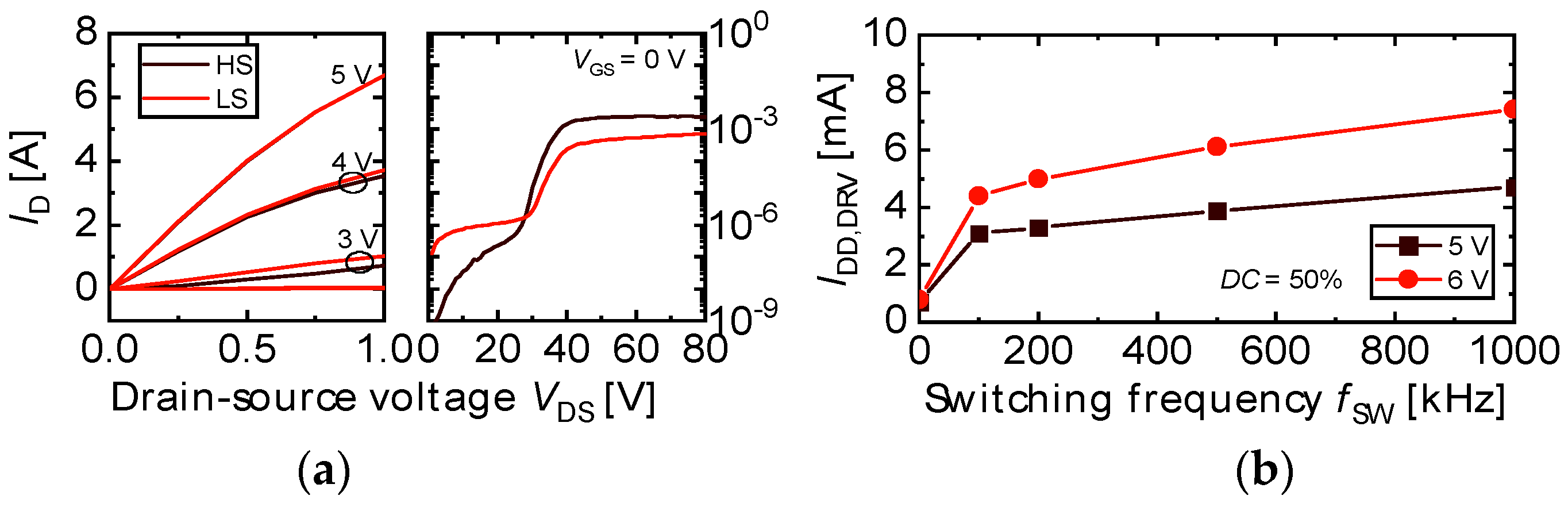
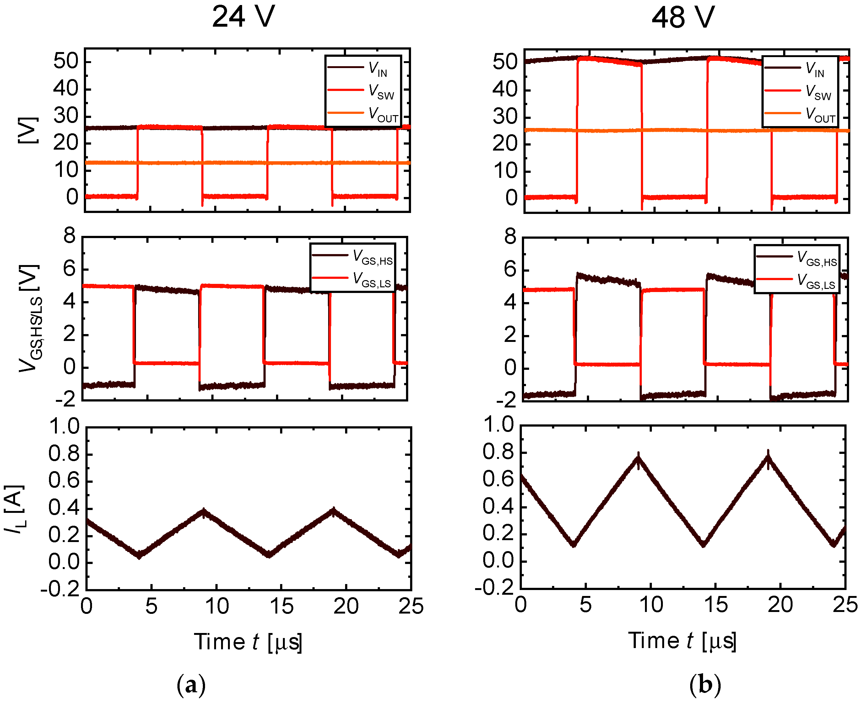
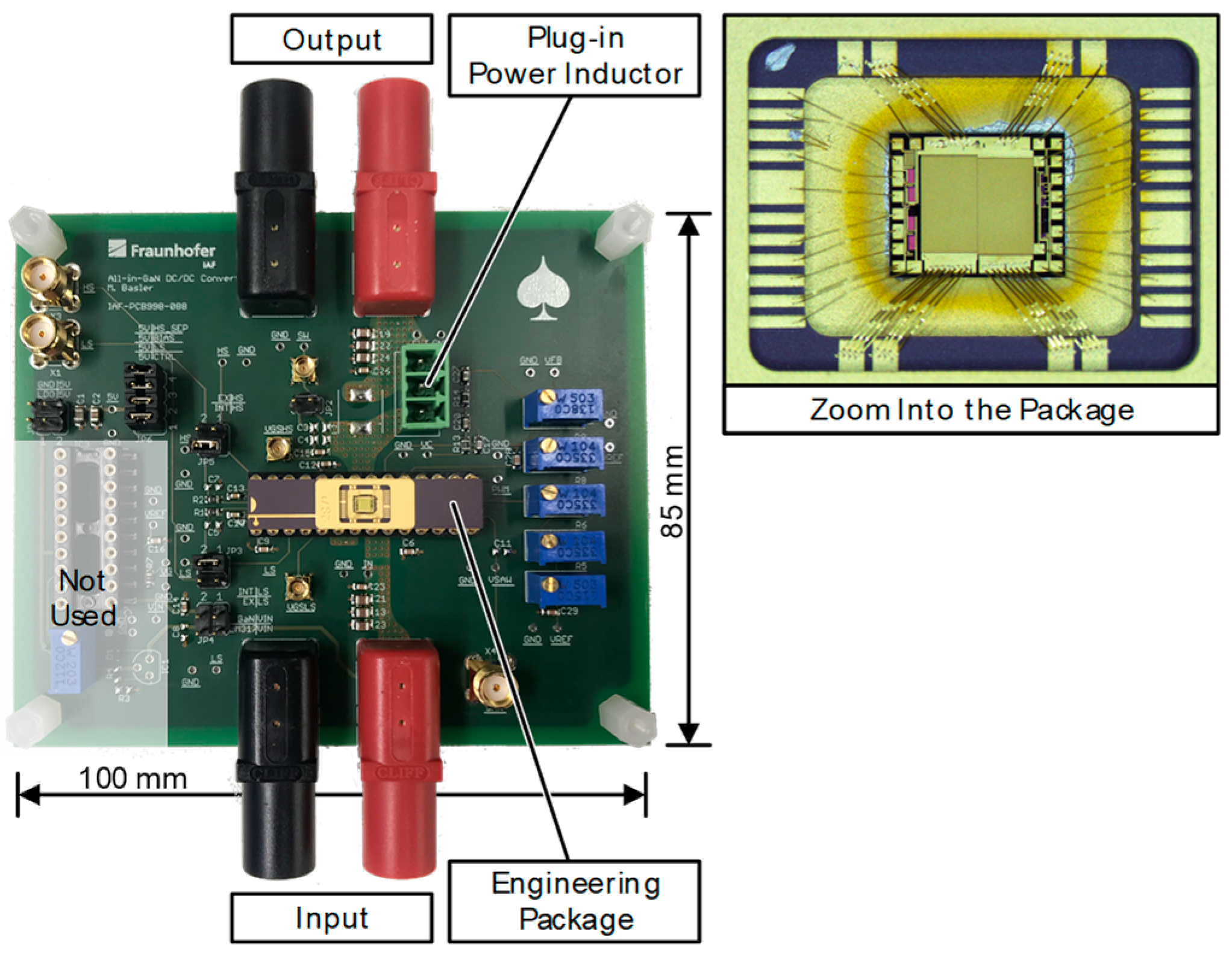
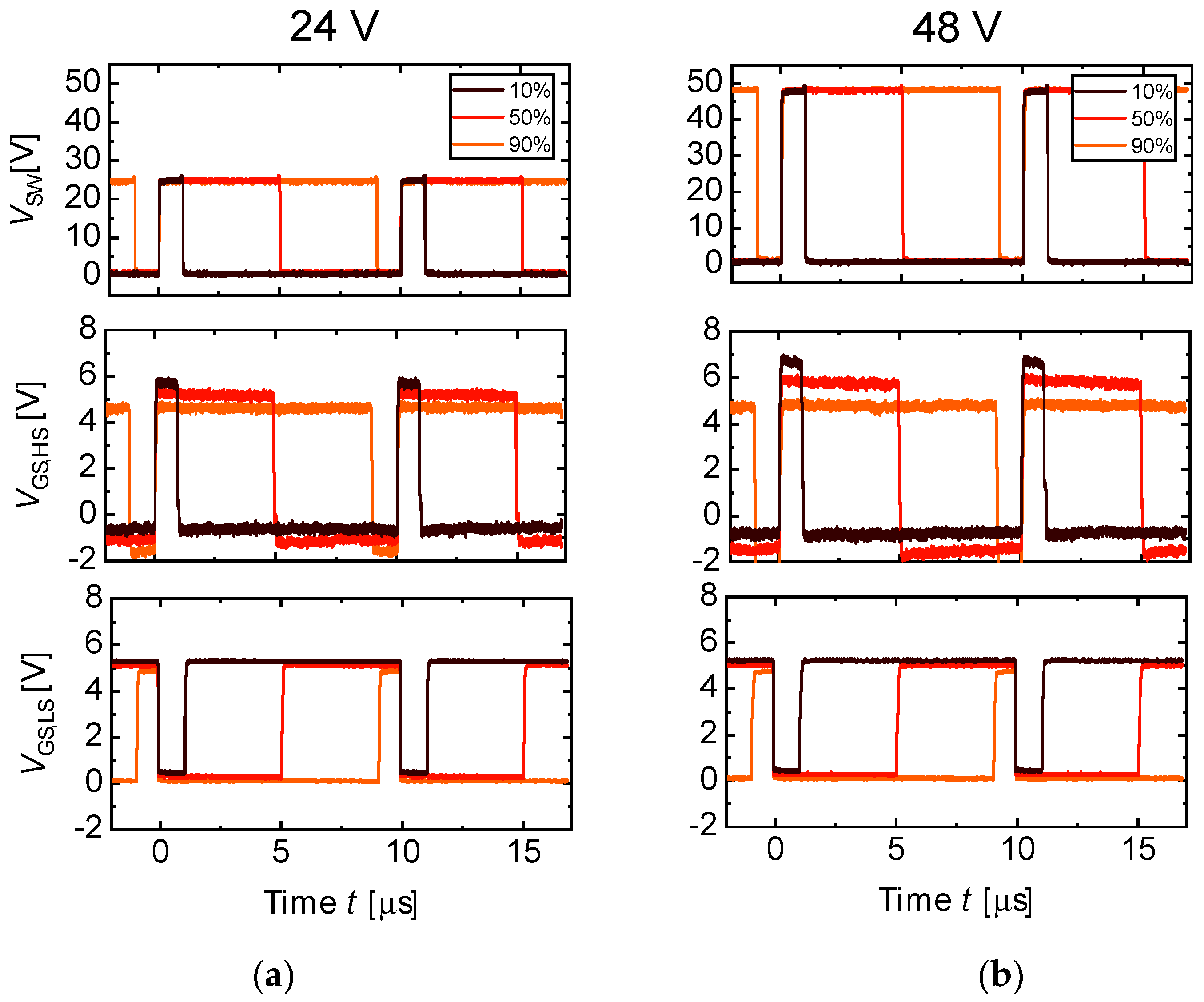
3. Measurement Results
4. Considerations on Life Cycle Assessment
5. Conclusions
Author Contributions
Funding
Data Availability Statement
Acknowledgments
Conflicts of Interest
References
- Chen, K.J.; Häberlen, O.; Lidow, A.; Tsai, C.l.; Ueda, T.; Uemoto, Y.; Wu, Y. GaN-on-Si Power Technology: Devices and Applications. IEEE Trans. Electron Devices 2017, 64, 779–795. [Google Scholar] [CrossRef]
- Jones, E.A.; Wang, F.F.; Costinett, D. Review of Commercial GaN Power Devices and GaN-Based Converter Design Challenges. IEEE J. Emerg. Sel. Top. Power Electron. 2016, 4, 707–719. [Google Scholar] [CrossRef]
- Wei, J.; Zheng, Z.; Tang, G.; Xu, H.; Lyu, G.; Zhang, L.; Chen, J.; Hua, M.; Feng, S.; Chen, T.; et al. GaN Power Integration Technology and Its Future Prospects. IEEE Trans. Electron Devices 2023, 71, 1365–1382. [Google Scholar] [CrossRef]
- Lidow, A. The Path Forward for GaN Power Devices. In Proceedings of the 2020 IEEE Workshop on Wide Bandgap Power Devices and Applications in Asia (WiPDA Asia), Suita, Japan, 23–25 September 2020; pp. 1–3. [Google Scholar]
- Kinzer, D. Monolithic GaN Power IC Technology Drives Wide Bandgap Adoption. In Proceedings of the 2020 IEEE International Electron Devices Meeting (IEDM), San Francisco, CA, USA, 12–18 December 2020; pp. 27.5.1–27.5.4. [Google Scholar]
- Basler, M.; Reiner, R.; Moench, S.; Benkhelifa, F.; Döring, P.; Waltereit, P.; Quay, R.; Ambacher, O. Building Blocks for GaN Power Integration. IEEE Access 2021, 9, 163122–163137. [Google Scholar] [CrossRef]
- Navitas Semiconductor. Sustainablility Report 2021: Electrify Our World™ GaNFast Power ICs Accelerate the Tranistion to Net Zero. Available online: https://navitassemi.com/wp-content/uploads/2022/03/Sustainability-Report-Brochure-v11.pdf (accessed on 21 September 2022).
- Efficient Power Conversion. EPC2152: 80 V, 15 A ePower™ Stage. Available online: https://epc-co.com/epc/Portals/0/epc/documents/datasheets/EPC2152_datasheet.pdf (accessed on 31 January 2022).
- Mönch, S.; Basler, M.; Reiner, R.; Benkhelifa, F.; Döring, P.; Sinnwell, M.; Müller, S.; Mikulla, M.; Waltereit, P.; Quay, R. GaN power converter and high-side IC substrate issues on Si, p-n junction, or SOI. E-Prime Adv. Electr. Eng. Electron. Energy 2023, 4, 100171. [Google Scholar] [CrossRef]
- Reiner, R.; Moench, S.; Waltereit, P.; Benkhelifa, F.; Basler, M.; Mikulla, M.; Quay, R. Design and Characterization of an Interleaved GaN Half-Bridge IC with Matrix Layout. In Proceedings of the PCIM Europe 2022: International Exhibition and Conference for Power Electronics, Intelligent Motion, Renewable Energy and Energy Management, Nuremberg, Germany, 4–6 May 2022; pp. 1–8. [Google Scholar]
- Basler, M.; Moench, S.; Reiner, R.; Benkhelifa, F.; Weidinger, G.; Weis, G.; Quay, R.; Kallfass, I.; Ambacher, O. High-Power Density DC-DC Converters Using Highly-Integrated Half-Bridge GaN ICs. In Proceedings of the PCIM Europe Digital Days 2021: International Exhibition and Conference for Power Electronics, Intelligent Motion, Renewable Energy and Energy Management, Nuremberg, Germany, 4–6 May 2021; pp. 1–8. [Google Scholar]
- Deckers, M.; Ravyts, S.; Vecchia, M.D.; Chatterjee, U.; Driesen, J. Comparison of GaN Enhancement Mode Transistor Performance with Integrated and External Driver. Power Electron. Devices Compon. 2022, 2, 100004. [Google Scholar] [CrossRef]
- Aygün, D.; Fossion, M.; Decoutere, S.; Barnes, A.; Delepaut, C.; Thoné, J.; Wens, M. A Monolithic 200V GaN Half Bridge IC with Integrated Gate Drivers and Level-shifters Achieving 98.3% Peak Efficiency. In Proceedings of the 2022 IEEE Applied Power Electronics Conference and Exposition (APEC), Houston, TX, USA, 20–24 March 2022; pp. 2141–2145. [Google Scholar]
- Wang, T.-W.; Kao, Y.-Y.; Hung, S.-H.; Wen, Y.-H.; Yang, T.-H.; Li, S.-Y.; Chen, K.-H.; Zheng, K.-L.; Lin, Y.-H.; Lin, S.-R.; et al. Monolithic GaN-Based Driver and GaN Switch with Diode-Emulated GaN Technique for 50-MHz Operation and Sub-0.2-ns Deadtime Control. IEEE J. Solid-State Circuits 2022, 57, 3877–3888. [Google Scholar] [CrossRef]
- Jiang, W.L.; Murray, S.K.; Zaman, M.S.; De Vleeschouwer, H.; Roig, J.; Moens, P.; Trescases, O. Monolithic Integration of a 5-MHz GaN Half-Bridge in a 200-V GaN-on-SOI Process: Programmable dv/dt Control and Floating High-Voltage Level-Shifter. In Proceedings of the 2021 IEEE Applied Power Electronics Conference and Exposition (APEC), Virtual, 14–17 June 2021; pp. 728–734. [Google Scholar]
- Basler, M.; Reiner, R.; Moench, S.; Waltereit, P.; Quay, R. Function Blocks of a Highly-Integrated All-in-GaN Power IC for DC-DC Conversion. In Proceedings of the 2022 24th European Conference on Power Electronics and Applications (EPE’22 ECCE Europe), Hannover, Germany, 5–9 September 2022; pp. 1–9. [Google Scholar]
- Strydom, J. Selecting eGaN® FET Optimal On-Resistance: White Paper WP011. Available online: http://epcco.com/epc/documents/papers/Selecting%20eGaN%20FET%20Optimal%20OnResistance.pdf (accessed on 17 January 2024).
- Basler, M.; Deneke, N.; Mönch, S.; Reiner, R.; Wicht, B.; Quay, R. Monolithically Integrated GaN Gate Drivers– A Design Guide. IEEE Open J. Power Electron. 2023, 4, 487–497. [Google Scholar] [CrossRef]
- Zheng, Y.; Li, B.; Dong, Q.; Ying, Y.; Song, D.; Zhu, J.; Sun, W.; Qian, Q.; Zhang, L.; Li, S.; et al. A 200-V Half-Bridge Monolithic GaN Power IC With High-Speed Level Shifter and TEXPRESERVE0 Noise Immunity Enhancement Structure. IEEE Trans. Very Large Scale Integr. (VLSI) Syst. 2023, 32, 542–551. [Google Scholar] [CrossRef]
- Qin, Y.; Ming, X.; Lin, Z.; Ye, Z.; Shi, J.; Zhuang, C.; Li, Z.; Zhang, B. A 50-V 50-MHz High-Noise-Immunity Capacitive-Coupled Level Shifter with Digital Noise Blanker for GaN Drivers. IEEE Trans. Circuits Syst. I Regul. Pap. 2023, 70, 2215–2227. [Google Scholar] [CrossRef]
- Zheng, Y.; Yuan, Q.; Song, D.; Ying, Y.; Zhu, J.; Sun, W.; Zhang, L.; Li, S.; Wang, D.; Zhou, J.; et al. A High-Speed Level Shifter with dVs/dt Noise Immunity Enhancement Structure for 200V Monolithic GaN Power IC. In Proceedings of the 2023 35th International Symposium on Power Semiconductor Devices and ICs (ISPSD), Hong Kong, 28 May–1 June 2023; pp. 203–206. [Google Scholar]
- Basler, M. Extended Monolithic Integration Levels for Highly Functional GaN Power ICs. Ph. D. Thesis, Albert-Ludwigs-University Freiburg, Freiburg, Germany, 2023. [Google Scholar]
- Chen, C.-J.; Wang, P.-Y.; Li, S.-T.; Chen, Y.-M.; Chang, Y.-C. An Integrated Driver with Bang-Bang Dead-Time Control and Charge Sharing Bootstrap Circuit for GaN Synchronous Buck Converter. IEEE Trans. Power Electron. 2022, 37, 9503–9514. [Google Scholar] [CrossRef]
- Zhuang, C.W.; Ming, X.; Ye, Z.K.; Qin, Y.; Lin, Z.Y.; Li, W.; Yan, H.; Zhang, B. Monolithic FET-Controlled GaN Driver with Pre-Boosting and Robust Dead Time Control for DToF LiDAR Application. In Proceedings of the 2023 35th International Symposium on Power Semiconductor Devices and ICs (ISPSD), Hong Kong, 28 May–1 June 2023; pp. 80–83. [Google Scholar]
- Kaufmann, M.; Wicht, B. A Monolithic GaN-IC With Integrated Control Loop for 400-V Offline Buck Operation Achieving 95.6% Peak Efficiency. IEEE J. Solid-State Circuits 2020, 55, 3169–3178. [Google Scholar] [CrossRef]
- EPA ENERGY STAR. ENERGY STAR Program Requirements for Computer Servers. Available online: https://www.energystar.gov/sites/default/files/specs//private/Computer_Servers_Program_Requirements%20v1.1.pdf (accessed on 23 January 2024).
- Reiner, R.; Basler, M.; Moench, S.; Waltereit, P.; Benkhelifa, F.; Mikulla, M.; Quay, R. Lateral GaN Power Devices and Integrated GaN Power Circuits: Status and Recent Progress. In Proceedings of the Components of Power Electronics and their Applications 2023, ETG Symposium, Bad Nauheim, Germany, 20–21 June 2023; pp. 89–96. [Google Scholar]
- Vauche, L.; Guillemaud, G.; Lopes Barbosa, J.-C.; Di Cioccio, L. Cradle-to-Gate Life Cycle Assessment (LCA) of GaN Power Semiconductor Device. Sustainability 2024, 16, 901. [Google Scholar] [CrossRef]
- Warren, J.A.; Riddle, M.E.; Graziano, D.J.; Das, S.; Upadhyayula, V.K.K.; Masanet, E.; Cresko, J. Energy Impacts of Wide Band Gap Semiconductors in U.S. Light-Duty Electric Vehicle Fleet. Environ. Sci. Technol. 2015, 49, 10294–10302. [Google Scholar] [CrossRef] [PubMed]


| [13] | [14] | [15] | This Work | |
|---|---|---|---|---|
| Technology | GaN-on-Si | GaN-on-SOI | GaN-on-SOI | GaN-on-Si |
| Int. Dead Time | Yes | Yes | No | Yes |
| Int. Control | Yes | No | No | Yes |
| Die size [mm2] | 16.75 | - | 5.26 1 | 7.5 |
| Power Supply [mW] | 13.8 | - | - | 26.4 |
| Max. VIN [V] | 48–400 | 200 | 50 | 80 |
| Max. IOUT [A] | 5 | 10 | 4 2 | |
| Max. POUT [W] | 240 | 223 | 100 | ≈100 2 |
| fSW [MHz] | ≤50 | 0.25–0.5 | ≤1 | ≤1 |
| ηPEAK [%] | 94.5 | 98.3 | 96 | - |
| Scenario |  |  | 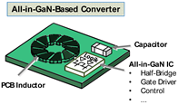 |
|---|---|---|---|
| Description | Discrete half-bridge with two Si MOSFETs | Discrete half-bridge with two GaN HEMTs | Monolithic GaN half-bridge with opt. int. driver, control, etc. |
| Control and driving | Si BCD/CMOS IC | Si BCD/CMOS IC | GaN (int. to the GaN half-bridge) |
| RON·A [mΩ·cm2] @100 V | 0.513 | 0.225 | 0.225 |
| RON·QG [mΩ·nC] @100 V | 288 | 31.2 | 31.2 |
| Price RON [€·Ω] @100 V | 1.33 × 10⁻² | 1.15 × 10⁻² | 1.15 × 10⁻² |
| El. req. for manufacturing | Si MOSFET: 2.45 2 | GaN: 2 3–2.43 | GaN: 2 3–2.43 |
| [kWh/cm2] 1 | Si BCD/CMOS: 0.67–3.02 | Si BCD/CMOS: 0.67–3.02 |
Disclaimer/Publisher’s Note: The statements, opinions and data contained in all publications are solely those of the individual author(s) and contributor(s) and not of MDPI and/or the editor(s). MDPI and/or the editor(s) disclaim responsibility for any injury to people or property resulting from any ideas, methods, instructions or products referred to in the content. |
© 2024 by the authors. Licensee MDPI, Basel, Switzerland. This article is an open access article distributed under the terms and conditions of the Creative Commons Attribution (CC BY) license (https://creativecommons.org/licenses/by/4.0/).
Share and Cite
Basler, M.; Mönch, S.; Reiner, R.; Benkhelifa, F.; Quay, R. Monolithically Integrated GaN Power Stage for More Sustainable 48 V DC–DC Converters. Electronics 2024, 13, 1351. https://doi.org/10.3390/electronics13071351
Basler M, Mönch S, Reiner R, Benkhelifa F, Quay R. Monolithically Integrated GaN Power Stage for More Sustainable 48 V DC–DC Converters. Electronics. 2024; 13(7):1351. https://doi.org/10.3390/electronics13071351
Chicago/Turabian StyleBasler, Michael, Stefan Mönch, Richard Reiner, Fouad Benkhelifa, and Rüdiger Quay. 2024. "Monolithically Integrated GaN Power Stage for More Sustainable 48 V DC–DC Converters" Electronics 13, no. 7: 1351. https://doi.org/10.3390/electronics13071351
APA StyleBasler, M., Mönch, S., Reiner, R., Benkhelifa, F., & Quay, R. (2024). Monolithically Integrated GaN Power Stage for More Sustainable 48 V DC–DC Converters. Electronics, 13(7), 1351. https://doi.org/10.3390/electronics13071351