Article

The Effect of Diluted N2O Annealing Time on Gate Dielectric Reliability of SiC Metal-Oxide Semiconductor Capacitors and Characterization of Performance on SiC Metal-Oxide Semiconductor Field Effect Transistor

1
School of Electronic Information, Hangzhou Dianzi University, Hangzhou 310018, China
2
Nanofabrication Facility, Suzhou Institute of Nano-Tech and Nano-Bionics, Chinese Academy of Sciences, Suzhou 215123, China
*
Authors to whom correspondence should be addressed.
Electronics 2024, 13(3), 596; https://doi.org/10.3390/electronics13030596
Submission received: 19 December 2023 / Revised: 27 January 2024 / Accepted: 29 January 2024 / Published: 31 January 2024
(This article belongs to the Section Semiconductor Devices)

Abstract

:
We performed dry oxidation on n-type silicon carbide (SiC), followed by annealing in diluted N2O, and subsequently fabricated n-type MOS structures. The study aimed to investigate the impact of different annealing times on the trap charges near the SiC/SiO2 interface and the reliability of the gate dielectric. Capacitance-voltage (C-V) and current-voltage (I-V) measurements of the n-type MOS revealed that increasing the annealing time with N2O effectively reduces the density of electron traps near the SiC/SiO2 interface, mitigates the drift in flat-band voltage and enhances the oxide breakdown field strength. However, excessive annealing time leads to an increase in the flat-band voltage drift of the MOS, resulting in premature oxide breakdown. Using the optimized annealing conditions, we fabricated n-type LDMOSFETs and obtained the threshold voltage (Vth), field-effect mobility (μFE) and specific on-resistance (Ron-sp) from the transfer curve (Id-Vg) and output curve (Id-Vd) measurements. The research findings provide valuable insights for the gate oxidation process of SiC.

1. Introduction

As one of the third-generation wide band gap semiconductors, Silicon carbide (SiC) has many outstanding electrical, mechanical and chemical properties, including a large band gap, high electron and hole mobility, extremely high hardness, high quality factor Q, high thermal conductivity, high chemical corrosion resistance and others [1]. Due to these physical advantages, SiC is now widely used as a material for powering MOSFET devices.
One advantage of SiC is that SiO2 can be obtained by thermal oxidation, which makes it possible to follow the similar design of silicon based on metal-oxide semiconductor (MOS) field effect transistors. However, a carbon-rich layer and defects form at the interface of SiC/SiO2 after oxidation. This results in a high density of interface states (Dit) near the conduction band edge (EC) and valence band edge (EV) in the SiC bandgap, trapping most of the free electrons in the MOSFET inversion channel, further reducing the channel mobility [2]. This is not good for MOSFET devices and can lead to an increase in the threshold voltage and power dissipation and a decrease in channel mobility. Different defect models have been proposed through theoretical calculations and experiments to explain the origin of the defects, such as the sub-oxide layer [3], native point defects [4] and carbon-related defects, including carbon-dangling bonds, SiCxOy species and carbon clusters [5,6]. Until now, there is still no consensus for a unified model of the dominating defects. For passivating these defects, conventional POA methods are used to passivate interface traps in a nitrogen-containing atmosphere (NO or N2O) [7,8]. N2O decomposes at a high temperature and produces NO and O2. NO will offer nitrogen for the interface, and the oxygen produced by N2O decomposition will cause slow re-oxidation. The competitive relationship between N passivation and re-oxidation makes the passivation effect of N2O slightly inferior to that of NO [9]. It is reported that the peak mobilities of MOSFETs annealed in NO and N2O were 37 and 29 cm2V−1s−1, respectively [10]. NO or N2O can provide a large amount of nitrogen during annealing. Nitrogen enters the SiC/SiO2 interface during annealing. As the annealing temperature or annealing time increases, this nitrogen accumulates at the SiC/SiO2 interface until saturation [11]. After reaching saturation, this nitrogen diffuses into the SiO2 and SiC bodies, filling silicon vacancies [12], reacting with carbon dangling bonds to convert C=C bonds into C=N bonds [13] and diffusing to the device channel region to form nitrogen doping [14], resulting in a reduction in the shallow interface state and improving the channel mobility of the device. Although annealing in NO has been proved to be more beneficial, N2O is still widely used, mainly because of the toxicity of NO [15]. The passivation effect is not only related to the annealing atmosphere but also closely related to the specific annealing conditions.
Many studies have shown that using diluted N2O to anneal the oxidized SiC/SiO2 interface can also improve the interface characteristics. The initial results by Philippe et al. show that the SiC MOS flat band voltage drift can be effectively reduced by cutting down the proportion of N2O in the annealing atmosphere from 20% to 10% [9]. Zhao et al. found that in the diluted N2O (10% in N2) annealing, a higher-temperature nitridation reduced the trap time constant and increased the trap capture cross-section [16]. Masato et al. annealed the SiO2 deposited by PECVD in diluted N2O. It was found that this annealing condition can improve the channel mobility of 4H-SiC MOSFETs [17]. Tseng et al. tested different mixing ratios between N2O and N2 at three temperatures to identify the mechanism of diluted N2O oxidation processes on 4H-SiC. The results demonstrated that the collision partner played a critical role in N2O decomposition. The diluent N2 worked as the collision partner at oxidation temperatures below 1200 °C and significantly affected the grown oxide thickness in a diluted N2O ambient [8].
Since a diluted N2O annealing process can weaken the re-oxidation and avoid the formation of new interface states, the influence of different annealing times in a diluted N2O atmosphere on the electrical performance of n-type SiC MOS capacitors was studied in this paper. Interface state density with charge voltage drift at different passivation times was extracted through C-V testing, characterizing the interface quality of SiC/SiO2. On the basis of SiC MOS capacitors, SiC LDMOSFET devices were fabricated to extract the channel mobility of MOSFET devices, quiescent electrical tests of MOSFET devices were carried out and the results were analyzed and calculated. The threshold voltage, transconductance, field-effect mobility and specific on-resistance were obtained and some existing research results were compared

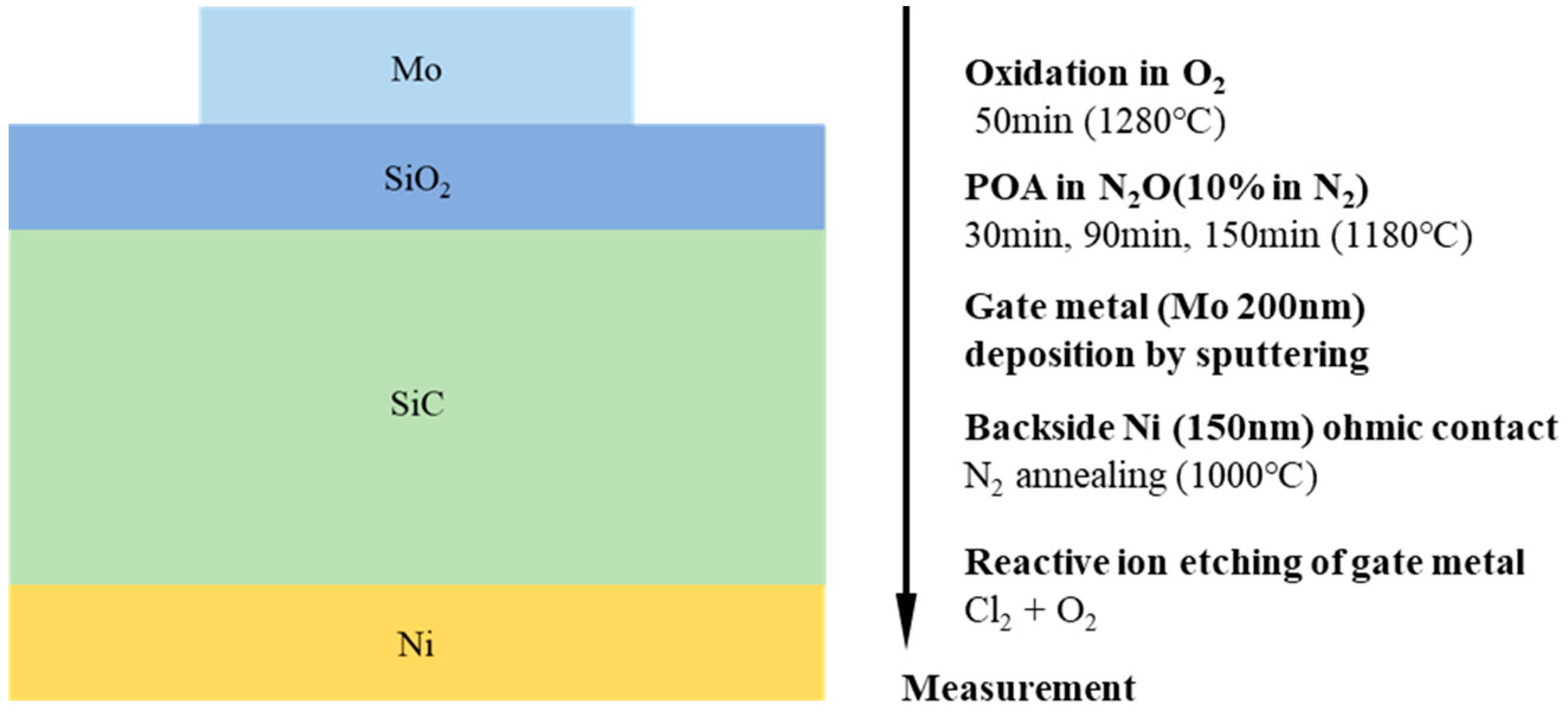
2. Experiment of MOS Capacitors

N2O is stable below 1100 °C, and when the temperature exceeds 1200 °C, N2O is thermally decomposed, and the reaction is as follows [1]:
N 2 O N 2 + O
N 2 O + O 2 NO
In the process of post-annealing, the diffusion coefficient of N2O in SiO2 is much lower than that of NO and O2 due to its large molecular weight, so the process of interfacial nitriding is not carried out by N2O itself but by NO produced by the thermal decomposition of N2O. This is consistent with the temperature required for N2O annealing in the industry from 1200 to 1300 °C. When the temperature exceeds 1300 °C, NO is also be decomposed by heat, which is not desirable, and the reaction of thermal decomposition is as follows:
2 NO N 2 + O 2
In this study, the MOS capacitors were fabricated on commercial n-type 4° off-axis (0001) 4H-SiC epitaxial wafers. The nitrogen doping concentration of the epitaxial layer was 8 × 1015 cm−3 and the thickness was 12 μm. The preparation process of the experiment is shown in Figure 1. The crystal elements were first cleaned with standard RCA and then immersed in BOE solution. The elements were then rinsed with deionized water and dried with nitrogen. After that, the gate oxides were fabricated by oxidation at 1280 °C for 50 min under dry oxygen pressure of 90 kPa. Then, different annealing times were used in diluted N2O (10% in N2O). The annealing temperature and pressure were 1180 °C and 90 kPa, respectively. After the annealing process, the molybdenum (Mo) film of 200 nm was deposited on the front of the sample as the gate electrode, while protecting the oxide layer from being affected by the subsequent process. The SiO2 on the back of the sample was removed by dry etching, and the 150 nm thick nickel (Ni) was then deposited as the back ohmic contact. Metal post-annealing was used in a N2 atmosphere at 1000 °C for 2 min. The photoresist was spun on Mo and graphically applied. Then, a metal dry etching machine was used to etch the excess Mo to form a circular gate electrode with a diameter of 300 μm.
The oxide thickness was measured by ellipsometry (J.A.WoollamM-2000, J.A Woollam, Lincoln, NE, USA) after annealing. The electrical properties of SiC MOS were measured by an Agilent-B1505A electrical characterization system. Near-interface traps (NITs) were characterized by bidirectional capacitance-voltage (C-V) measurement at room temperature. The voltage sweep started from depletion towards accumulation, followed by a reverse sweep from accumulation towards depletion. The interface state density (Dit) was extracted by the high frequency–low frequency method. The current-voltage (I-V) curve was obtained by applying a DC voltage with a step size of 0.1 V to characterize the reliability of the gate oxide. Twenty MOS electrodes were designed in the experiment, and the average value was taken as the test results under the corresponding oxidation conditions.

3. Results and Discussion

This section is divided by subheadings. It should provide a concise and precise description of the experimental results and their interpretation, as well as the experimental conclusions that can be drawn.

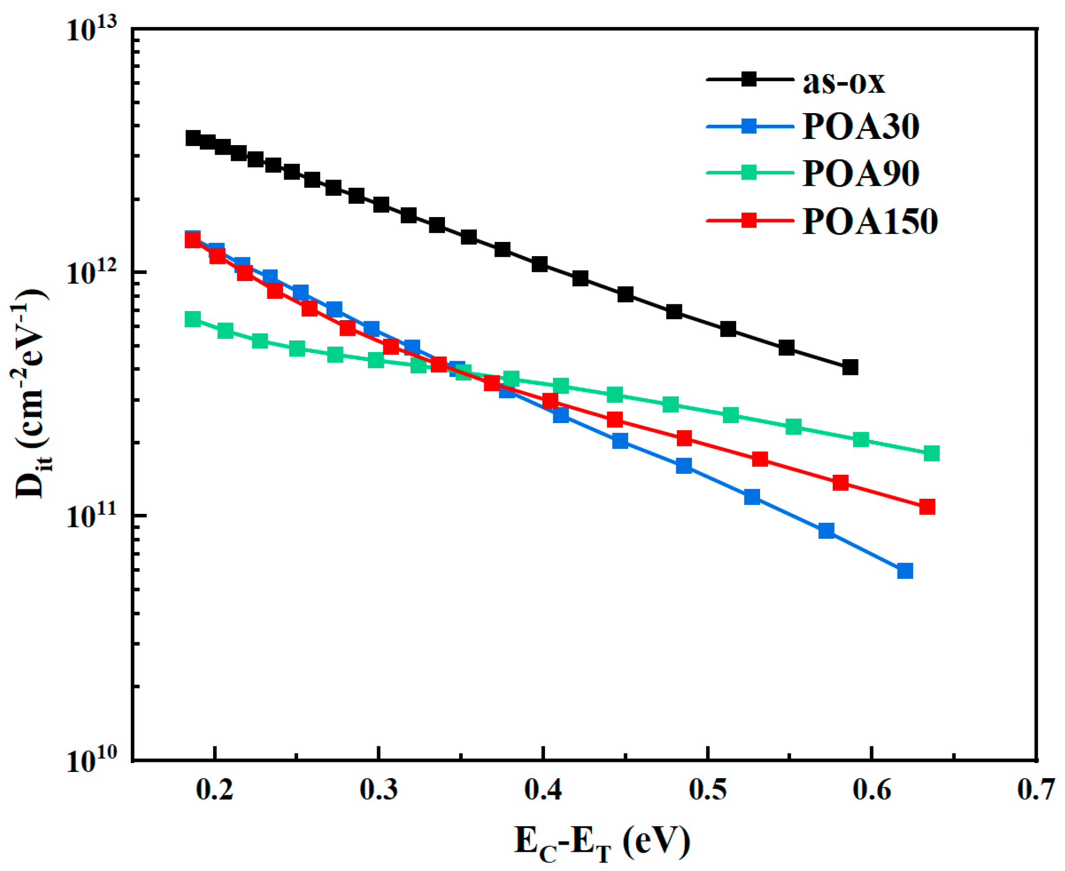
3.1. The Results of C-V Test

After oxidation and annealing, ellipsometry measurements show that the oxide thicknesses of as-ox, POA30, POA90 and POA150 are 47.2 nm, 48.4 nm, 48.6 nm and 49.4 nm, respectively. It can be seen that when annealed in diluted N2O, the thickness change of the sample’s oxide layer is negligible. This avoids additional oxidation, which might lead to new interface traps [17].
The normalized bidirectional C-V measurement results with a frequency of 1 MHz are shown in Figure 2. The C-V curves of all samples have positive flat-band voltage. This indicates that negative charges were generated during the preparation process of the SiC MOS capacitor. The sample without annealing shows a flat band voltage of 4.71 V. After N2O annealing, the curve had obvious left shift and clockwise hysteresis. This is determined by the doping concentration of SiC and the work function of the gate electrode, indicating the presence of negative fixed charges and electron traps. The hysteresis of the curve is related to the oxide trap near the interface. When the gate voltage scans from negative to positive, electrons are injected into the oxide and captured by NITs [18]. Then, when the gate voltage is retraced, these electrons cannot be released in time due to their large time constant [19]. A larger gate voltage was needed to balance these electrons. According to the bidirectional C-V curve, the flat band voltage and the trap density near the interface were extracted, as shown in Table 1. At the annealing time of 30 min, the density of the NITs was 5.27 × 1010 cm−2. When the time was increased to 90 min, the density of the NITs was increased to 2.11 × 1011 cm−2. When annealed for 150 min, the density of the NITs was close to the value of the un-annealed one. This indicates that the flat band voltage and hysteresis voltage decreases with the increase in annealing time in diluted N2O. However, excessive annealing also increases the flat band voltage and hysteresis voltage. This is because N2O decomposes at a high temperature to produce NO, O2 and N2, and the NO injects N atoms into the interface. The accumulation of N atoms reduces the density of interface states and NITs [15]. After annealing in N2O, the interface of SiC/SiO2 is nitride. At the interface after nitriding, it was found that when the temperature drops to 4 K, there was a very strong EDMR signal generated by Nh, which was similar to the nitrogen shallow donor at the 4H SiC carbon h-site [NC(h); C3v symmetry, g = 2.0005 and g = 2.0010 ] [20]. The signal width of this Nh was only 0.4–0.5 mT, which was much smaller than the 3.6 mT [20] of the k-site shallow nitrogen donor NC(k), This indicates that both of the NC(h) and Nh centers are related to shallow nitrogen donors. When the temperature was less than 20 K, the relationship between NC(h) and Nh was consistent. Therefore, it is believed that the Nh signal originates from the h-site of the shallow nitrogen donor in the channel region. The annealing time and temperature in N2O atmosphere can both affect the concentration of N at the SiC/SiO2 interface. With the increase in annealing time and temperature, the concentration of N at the SiC/SiO2 interface significantly increases. After reaching saturation, it diffuses into SiO2 and SiC. The XPS measurement results show that the N peak widens as the concentration of N atoms increases [21]. During the annealing process, these N atoms that diffuse to the surface of SiC form high-density N donors and ultimately appear in the form of Nh centers. These shallow interface state donors form very fast interface states near the conduction band (EC). Compared to slow interface states that can be detected at a frequency of 1 M, these very fast interface states often require a frequency of over 100 M to be detected or can be detected at a frequency of around 1M when the temperature is lowered to low temperatures (<20 K). The interface state of the SiC/SiO2 interface decreases due to the accumulation of N at the interface during annealing, but at the same time, very fast interface states are also generated, which is a dynamic process that requires finding an equilibrium point. These diffused N atoms form stable binding states that exist at the interface, even if they are γ -ray exposure does not remove it, and the specific form of existence still needs to be studied. When these N donors appear in the channel region, it is obvious that this lowers the threshold voltage of the device [20,22]. Therefore, by properly controlling the N2O annealing time, SiC MOSFET can perform with relatively low threshold voltage and small threshold voltage drift.
The channel mobility of SiC MOSFET is low because the high density of states (Dit) at the SiC/SiO2 interface causes Coulomb scattering [23]. The Dit was extracted by the high–low method at EC − ET = 0.2–0.6 eV [24]. The characteristics of high frequency and low frequency were measured at 1 MHz and 1 kHz, respectively. When a high frequency signal is added to a DC signal, the interface defects cannot catch and release electrons following the signal. When a low frequency signal is superimposed, interface defects can trap and release electrons. Figure 3 shows the Dit distribution of the SiC MOS capacitors near the edge of the 4H-SiC conduction band at different annealing times. The POA90 sample has the lowest Dit of 5.78 × 1011 cm−2eV−1 when EC − ET = 0.2 eV.
The accumulation of N atoms on the SiC/SiO2 interface during annealing can remove the C-related defects and form stronger Si≡N and O≡N bonds [25]. During the oxidation process of SiC, carbon splitting gaps may be formed, some of which may form π-bonded interstitial carbon dimers (Ci=Ci) during the oxidation process. These Ci=Ci dimers may generate acceptor states near the edge of CB. When annealing in a N2O atmosphere, NO generated by thermal decomposition enters the SiC/SiO2 interface and react with Ci=Ci within a certain Fermi level range, as shown in the following formula [13]:
SiC / SiO 2 : [ C i = C i ) 0 + 2 e + SiO 2 : NO SiC / SiO 2 : C i C + O if 0 + SiO 2 : C N
SiC / SiO 2 : [ C i = C i ) 0 + e + SiO 2 : NO SiC / SiO 2 : ( N i = C i ) + + SiO 2 : C O 2
Equation (4) gives an energy gain of 2EF − 1.3 eV, i.e., 2.5–3.1 eV in the chosen Fermi-level range and describes the observed carbon removal from the interface [9,26]. The energy gain in Equation (5) is EF + 1.8 eV, positive for any Fermi-level position, and 3.7–4.0 eV in our range. Therefore, this is the dominant reaction and it is responsible for the observed nitrogen incorporation at the interface [27]. These reactions convert the carbon dimer into a zwitterionic but mobile carbon filler and into a fixed N=C dimer (deep donor level), with a few N=N bonds expected [13]. When annealed in the atmosphere containing N2O, the passivation by N and the oxidation by oxygen are carried out simultaneously. Even if N2O was diluted, additional oxidation still exists [8,28]. When the annealing time increased to 150 min, the Dit increased instead. The content of N atoms at the interface tends to become saturated. Excessive nitrogen passivation causes nitrogen atoms to diffuse into the SiO2 layer for several nanometers near the interface. This leads to some new interface traps, decreasing the field effect mobility (μFE) of MOSFET [29]. The value of Dit of the POA90 and POA150 samples at EC − ET = 0.35–0.6 eV is larger than that of POA30. The energy level of the C cluster is related to its size [13]. The passivation of N can reduce the size of C clusters and transfer their energy levels to the lower part of the semiconductor band gap (or possibly beyond the band gap) [30]. Therefore, the Dit between 0.35 and 0.6 eV at the bottom of the conduction band increases. The longer nitrogen passivation of the POA150 sample makes Dit lower than that of the POA90 sample at EC − ET = 0.35–0.6 eV.

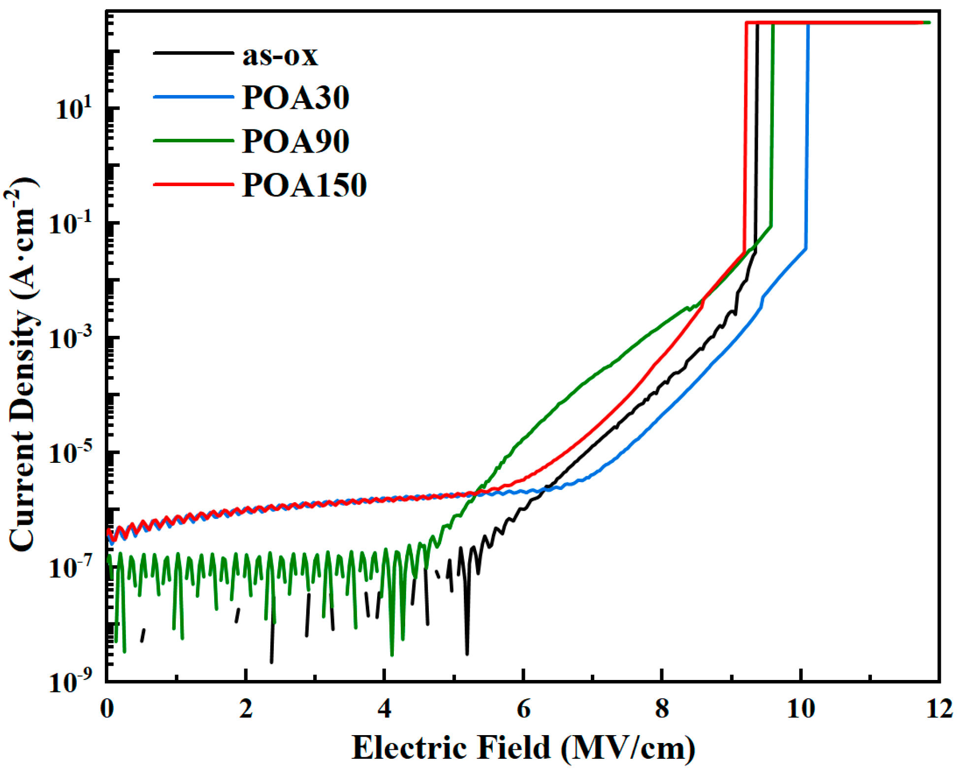
3.2. The Results of IV Test

Figure 4 shows the leakage current density–electric field (J-E) curve of the SiC MOS capacitor under different annealing times. The POA30 sample has the highest breakdown field of 10.08 MV/cm. Although increasing the annealing time is helpful to reduce the density of interface states and improve the mobility of devices, the reliability of the gate dielectric is be reduced at the same time and makes the gate breakdown prematurely. The longer the passivation time is, the earlier the dielectric breakdown point arrives. These results show that the oxide leakage current density at electric fields above 5 MV/cm increases sharply due to Fowler–Nordheim tunneling; when a positive voltage is applied to the gate of an n-channel MOS capacitor, an electric field appears in the gate oxide layer. At low electric fields, due to the presence of a potential barrier between the semiconductor and the metal, the current density remains almost unchanged. When the gate voltage rises and the oxide layer is in the high field region, the height and width of the barrier decrease, and the probability of electrons tunneling through the oxide layer from the semiconductor into the metal greatly increase; this significantly increases the current density between the semiconductors and metals. The electron tunneling model under high electric fields is called the Fowler–Nordheim tunneling model, and the leakage current is controlled by this model. Its expression is as follows [1]:
J FN = q 3 E 2 16 π ϕ B exp ( 4 2 m * ϕ B 3 3 q E )
Among them, E is the electric field strength in the oxide, m * is the effective mass of electrons in the oxide, ϕ B is the barrier height or conduction band offset between the oxides and semiconductors ( Δ E C ) and = h / 2 π , where h is the Planck constant. From this, it can be seen that as the electric field strength increases, the leakage current controlled by the Fowler–Nordheim tunneling model significantly increases. As shown in Figure 4 of the article, except for POA30 and POA150, samples of as-ox and POA90 experience a sharp increase in leakage current above 5MV/cm due to the Fowler–Nordheim tunneling effect. So, the electric field in the oxide layer of all samples should be kept below 5 MV/cm.

4. Experiment of LDMOSFETs

LDMOSFETs were fabricated on commercial n-type 4° off-axis (0001) 4H-SiC epitaxial wafers. The nitrogen doping concentration of the epitaxial layer was 8 × 1015 cm−3 and the thickness was 12 μm. Firstly, the inorganic solution was used to clean the substrate according to RCA standard to remove the dirt on the surface, and then the BOE solution was used to remove the natural oxide layer on the substrate to prevent the oxide layer from affecting the subsequent process. The tablets were then washed with deionized water and blown dry with nitrogen for the subsequent steps. In the first step, high-temperature ion implantation was carried out, and AlCl3 was used as the P-type injection source to form a P-base region at a depth of 750 nm with a doping concentration of 1 × 1017 cm−3. The second step was still high-temperature ion implantation, using N as the N-type injection source, and the injection was formed into a N + source region with a depth of 300 nm and an injection concentration of 1 × 1019 cm−3. Ion implantation was followed by high-temperature ion activation, which was first baked with photoresist to form a carbon film, which was covered on the surface of the substrate, and then annealed in an argon atmosphere at 1700 °C for 30 min. After completion, the degumming machine was used for 10 min under a condition of 500 W to remove the carbon film on the surface. After that, the sacrificial oxidation of the surface was carried out, and the surface was oxidized with SiC of about 20 nm to ensure the flatness of the surface and reduce the effect of ion implantation on the substrate surface. After that, the gate oxygen layer was formed by oxidation at 1280 °C for 50 min in the oxidation equipment, and immediately after the oxidation, it was annealed at 1180 °C for 0, 30, 90 and 150 min in the same equipment using a diluted N2O atmosphere (as-ox, POA30, POA90, POA150). After the gate oxygen preparation was completed, 500 nm of metal Mo was sputtered on the surface, and the gate electrode was prepared by the stripping process. Then, 500 nm of metal Ni was sputtered to form a source-drain metal at 1000 °C. The general fabrication process and device structure are illustrated in Figure 5. Upon device fabrication completion, testing was carried out using Agilent B1505 (Agilent, Santa Clara, CA, USA). The I-V test of the transfer characteristics and output characteristics of the LDMOSFET device was carried out, and the threshold voltage and transconductance were extracted from the obtained transfer characteristic curves. The field-effect mobility of the device was calculated by using the transconductance. The specific on-resistance was obtained from the resulting output characteristic curve. Twenty MOSFETs were designed in the experiment, and the average value was taken as the test results under the corresponding oxidation conditions.

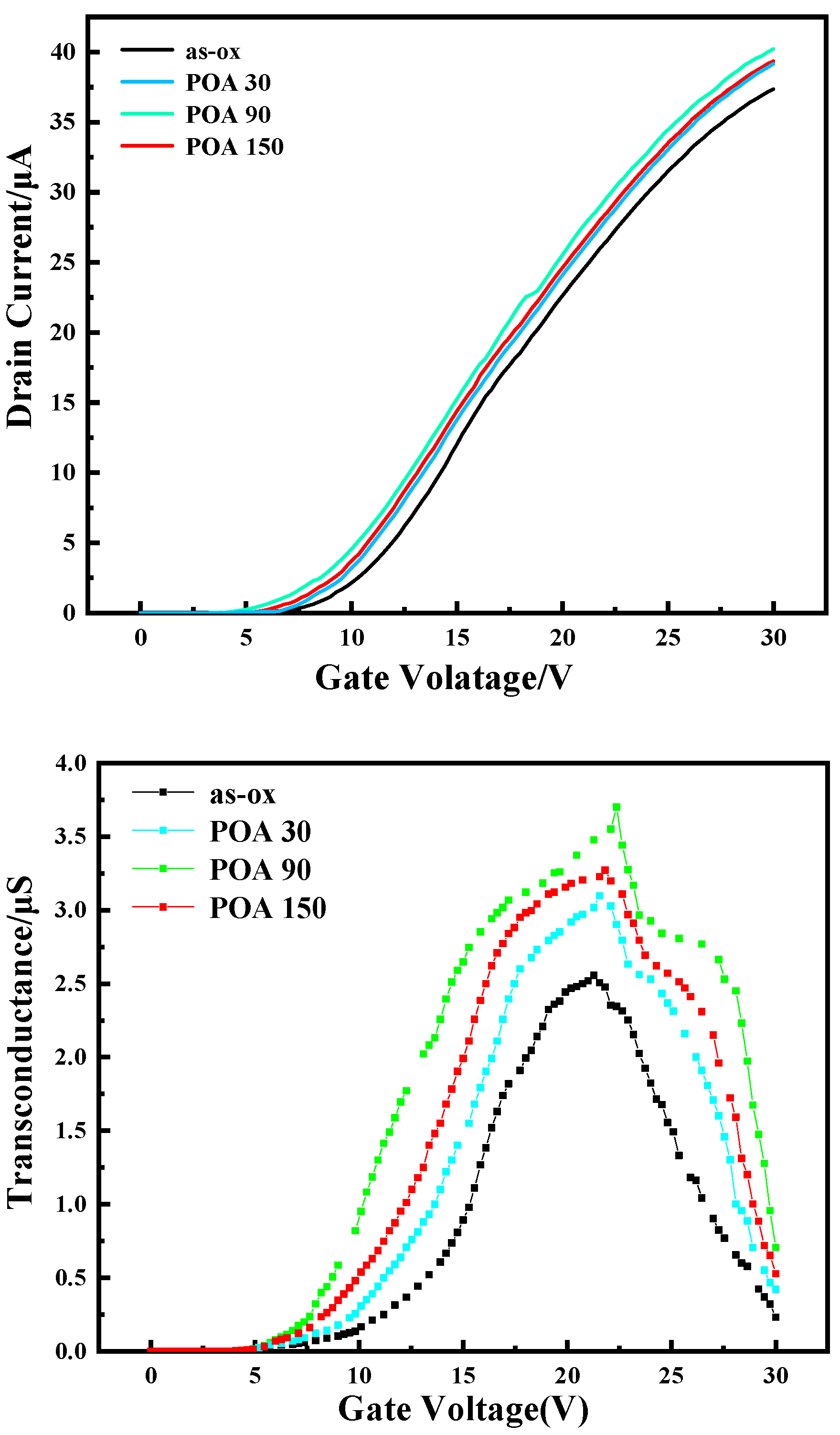
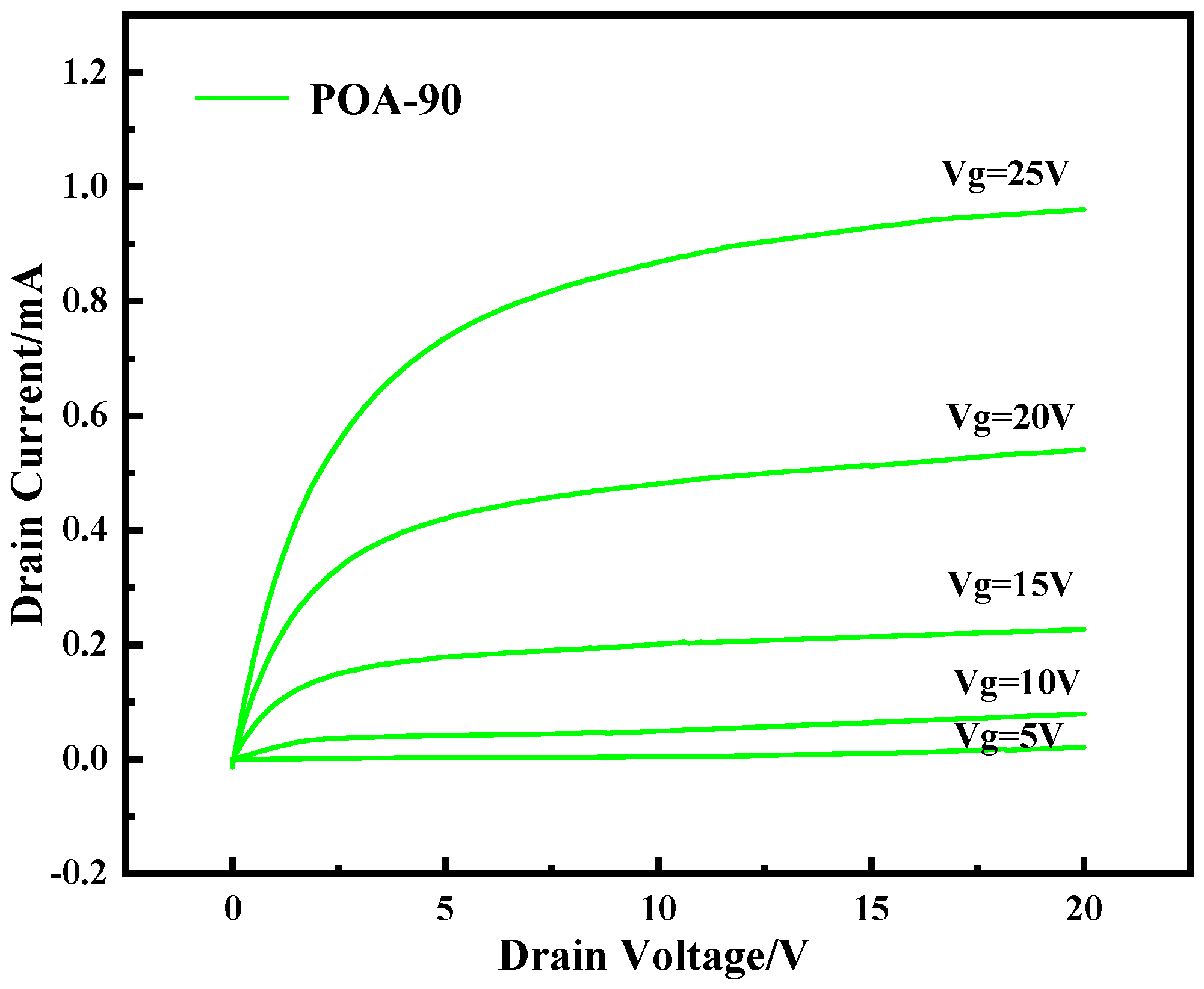
The Results of I-V Test

The transfer curve is shown in Figure 6. The graph shows the curves of as-ox, POA-30, POA-90 and POA-150. Taking POA-90 as an example, the threshold voltage of 7.83 V is obtained by linear extrapolation from the linear region of the transfer characteristics. The peak transconductance of the device is 3.79 μS at Vg = 24V. Figure 7 shows the typical output characteristics of the fabricated lateral enhancement mode N-channel MOSFET using POA-90 as an example, with the gate voltage (Vg) from 0 V to 25 V and the drain– source voltage (VDS) from 0 V to 20 V. The device exhibits a drain current of 1010 µA at Vg = 25 V and VDS = 20 V. The output characteristics exhibit excellent linear and saturation regions. The specific data are shown in Table 2.
To verify the effectiveness of annealing in diluted N2O and the effect of different annealing times on device performance, the gate voltage dependence of the field-effect mobility µFE was measured, and the Vg for the measurement ranged from 0 to 30 V. The µFE can be calculated from the following formula using transconductance characteristics at a drain voltage of 100 mV [1]:
μ F E = I d V g s C o x V d s W L
In this context, (∂Id)/(∂Vgs) is the transconductance, also denoted as “gm”, Cox represents the gate oxide capacitance, W stands for channel width and L signifies channel length. In the fabricated devices, the gate oxide thickness, channel length and channel width are 49.6 nm, 2 μm and 150 μm, respectively. Taking LDMOSFET devices prepared under POA90 conditions as an example, the calculations reveal a peak field-effect mobility of 7.1 cm2/V·s for the device. The output curve is depicted in Figure 7, and by evaluating the linear region with a source-drain voltage from 0 to 3 V, the specific on-resistance of the device is calculated to be 12 mΩ·cm2.
The results indicate that the annealing time in N2O does not necessarily present a trend of the longer the better. An excessively long annealing time can actually increase the interface state density and reduce the peak field effect mobility of the device, which is consistent with the conclusion of MOS capacitors. However, the peak field effect migration rate of POA-90 is not particularly prominent compared to current research levels, which may be due to several reasons: firstly, differences in annealing atmosphere. Many studies have used a NO annealing atmosphere, while this article uses a N2O annealing atmosphere. Compared with NO annealing, the N2O annealing process involves re-oxidation, and the impact on the interface state during this process is more complex. Secondly, this may be a problem with the preparation process. In this article, the N2O annealing process is directly carried out after gate oxygen oxidation, while in other studies, such as Song et al.’s [31], the gate oxygen preparation process issandwich (nitridation–oxidation–nitridation) type. Different preparation processes result in different SiO2/SiC interfaces, which have a significant impact on the device. Thirdly, due to process limitations, this article chose metal Mo instead of polycrystalline silicon as the gate metal. Polysilicon can change the Fermi level through high concentration doping, which can adjust the barrier height during the metal oxide semiconductor contact process, making it more suitable as the gate of MOSFET. Although the peak field effect mobility of the device prepared in this article is not high, the structure proposed in this article has a smaller threshold voltage compared to the study by Song et al. The process of gate oxygen preparation and oxidation mentioned in this article is also relatively simple, and simpler process steps introduce fewer errors, which is conducive to achieving better device performance. The conclusion of this article has certain guiding significance for the preparation of SiC MOSFET devices.

5. Conclusions

In this paper, n-type SiC MOS was prepared to study the effect of different N2O annealing times on the reliability of MOS gate dielectrics. Through C-V test, it was found that with the increase in annealing time, the flat band voltage and the density of states at the SiC/SiO2 interface decreased. However, a too-long N2O annealing time will lead to excessive nitrogen passivation and additional oxidation, which will increase NITs and Dit. The I-V test showed that a shorter annealing time is helpful to improve the breakdown field of gate dielectrics. Annealing in diluted N2O needs to be comprehensively considered for its influence on threshold voltage, channel mobility and dielectric breakdown field. The experimental results of n-channel SiC MOS capacitors show that the interface state density of Ec − Et = 0.2 eV of POA90 is the smallest. LDMOSFET devices were prepared using different annealing conditions, and the transfer and output characteristics of the devices were measured. The results showed that post annealing in a N2O atmosphere can improve the performance of the devices, such as the threshold voltage and peak field effect mobility. However, the longer the annealing time, the more complex the interface state of SiO2/SiC and the lower the device performance. Based on the experimental results of MOS capacitors, POA90 has the minimum interface density of states at Ec − Et = 0.2 eV, as well as the lowest threshold voltage and highest field effect mobility. The research results of this article have certain reference significance for the manufacturing process of MOSFET devices.

Author Contributions

Methodology, L.J., M.S., C.Z., H.L., Y.S. and Q.C.; Software, L.J. and H.L.; Formal analysis, M.S. and C.Z.; Resources, Z.D., C.Z., Z.Z. and B.Z.; Writing—original draft, L.J. and H.L.; Writing—review & editing, Z.D. and B.L. All authors have read and agreed to the published version of the manuscript.

Funding

This research received no external funding.

Data Availability Statement

Data are found within the article.

Conflicts of Interest

The authors declare no conflict of interest.

References

  1. Kimoto, T.; Cooper, J.A. Fundamentals of Silicon Carbide Technology: Growth, Characterization, Devices and Applications; John Wiley & Sons: Singapore, 2014. [Google Scholar]
  2. Dhar, S. Nitrogen and hydrogen induced trap passivation at the SiO2/4H-SiC interface. In Materials Science Forum; Trans Tech Publications Ltd.: Stafa-Zurich, Switzerland, 2006; pp. 949–954. [Google Scholar]
  3. Li, X.; Lee, S.S.; Li, M.; Ermakov, A.; Medina-Ramos, J.; Fister, T.T.; Amarasinghe, V.; Gustafsson, T.; Garfunkel, E.; Fenter, P.; et al. Effect of nitrogen passivation on interface composition and physical stress in SiO2/SiC (4H) structures. Appl. Phys. Lett. 2018, 113, 131601. [Google Scholar] [CrossRef]
  4. Kobayashi, T.; Harada, K.; Kumagai, Y.; Oba, F.; Matsushita, Y.I. Native point defects and carbon clusters in 4H-SiC: A hybrid functional study. J. Appl. Phys. 2019, 125, 125701. [Google Scholar] [CrossRef]
  5. Anders, M.A.; Lenahan, P.M.; Lelis, A.J. Are dangling bond centers important interface traps in 4H-SiC metal oxide semiconductor field effect transistors. Appl. Phys. Lett. 2016, 109, 142106. [Google Scholar] [CrossRef]
  6. Devynck, F.; Alkauskas, A.; Broqvist, P.; Pasquarello, A. Charge transition levels of carbon-, oxygen-, and hydrogen-related defects at the SiC/SiO2 interface through hybrid functionals. Phys. Rev. B 2011, 84, 235320. [Google Scholar] [CrossRef]
  7. Tseng, Y.H.; Wu, T.H.; Tsui, B.Y.; Yen, C.T.; Hung, C.C.; Lee, C.Y. A comprehensive study on the oxidation of 4H-SiC in diluted N2O ambient. Jpn. J. Appl. Phys. 2017, 56, 04CR02. [Google Scholar] [CrossRef]
  8. Zhai, D.; Gao, D.; Xiao, J.; Gong, X.; Yang, J.; Zhao, Y.; Wang, J.; Lu, J. Electrical characterization of near-interface traps in thermally oxidized and NO-annealed SiO2/4H-SiC metal-oxide-semiconductor capacitors. J. Phys. D Appl. Phys. 2020, 53, 445102. [Google Scholar] [CrossRef]
  9. Jamet, P.; Dimitrijev, S.; Tanner, P. Effects of nitridation in gate oxides grown on 4H-SiC. J. Appl. Phys. 2001, 90, 5058–5063. [Google Scholar] [CrossRef]
  10. Nanen, Y.; Kato, M.; Suda, J.; Kimoto, T. Effects of nitridation on 4H-SiC MOSFETs fabricated on various crystal faces. IEEE Trans. Electron Devices 2013, 60, 1260–1262. [Google Scholar] [CrossRef]
  11. Yoshioka, H.; Nakamura, T.; Kimoto, T. Generation of very fast states by nitridation of the SiO2/SiC interface. J. Appl. Phys. 2012, 112, 024520. [Google Scholar] [CrossRef]
  12. Meyer, D.J.; Bohna, N.A.; Lenahan, P.M.; Lelis, A.J. Spin dependent recombination at deep-level centers in 6H silicon carbide/silicon metal oxide semiconductor field effect transistors. In Materials Science Forum; Trans Tech Publications Ltd.: Bäch, Switzerland, 2004; Volume 457, pp. 477–480. [Google Scholar] [CrossRef]
  13. Deak, P.; Knaup, J.M.; Hornos, T.; Thill, C.; Gali, A.; Frauenheim, T. The mechanism of defect creation and passivation at the SiC/SiO2 interface. J. Phys. D Appl. Phys. 2007, 40, 6242. [Google Scholar] [CrossRef]
  14. Agarwal, A.K.; Burk, A.A.; Callanan, R.; Capell, C.; Das, M.K.; Haney, S.K.; Hull, B.A.; Jonas, C.; O’Loughlin, M.J. Critical technical issues in high voltage SiC power devices. In Materials Science Forum; Trans Tech Publications Ltd.: Bäch, Switzerland, 2009; Volume 600, pp. 895–900. [Google Scholar] [CrossRef]
  15. Siddiqui, A.; Elgabra, H.; Singh, S. The current status and the future prospects of surface passivation in 4H-SiC transistors. IEEE Trans. Device Mater. Reliab. 2016, 16, 419–428. [Google Scholar] [CrossRef]
  16. Zhao, P.; Liu, Y.; Tin, C.C.; Zhu, W.G.; Ahn, J. Investigation of 4H-SiC MOS capacitors annealed in diluted N2O at different temperatures. Microelectron. Eng. 2006, 83, 61–64. [Google Scholar] [CrossRef]
  17. Noborio, M.; Suda, J.; Kimoto, T. P-Channel MOSFETs on 4H-SiC {0001} and Nonbasal Faces Fabricated by Oxide Deposition and N2O Annealing. IEEE Trans. Electron Devices 2009, 56, 1953–1958. [Google Scholar] [CrossRef]
  18. Jia, Y.; Lv, H.; Song, Q.; Tang, X.; Xiao, L.; Wang, L.; Tang, G.; Zhang, Y.; Zhang, Y. Influence of oxidation temperature on the interfacial properties of n-type 4H-SiC MOS capacitors. Appl. Surf. Sci. 2017, 397, 175–182. [Google Scholar] [CrossRef]
  19. Luo, Z.; Wan, C.; Jin, Z.; Xu, H. Effects of sequential annealing in low oxygen partial-pressure and NO on 4H-SiC MOS devices. Semicond. Sci. Technol. 2021, 36, 045021. [Google Scholar] [CrossRef]
  20. Greulich-Weber, S. The microscopic and electronic structure of shallow donors in SiC. Phys. Status Solidi (b) 1998, 210, 415–427. [Google Scholar] [CrossRef]
  21. Fujihira, K.; Tarui, Y.; Imaizumi, M.; Ohtsuka, K.I.; Takami, T.; Shiramizu, T.; Kawase, K.; Tanimura, J.; Ozeki, T. Characteristics of 4H–SiC MOS interface annealed in N2O. Solid-State Electron. 2005, 49, 896–901. [Google Scholar] [CrossRef]
  22. Umeda, T.; Esaki, K.; Kosugi, R.; Fukuda, K.; Ohshima, T.; Morishita, N.; Isoya, J. Behavior of nitrogen atoms in SiC-SiO2 interfaces studied by electrically detected magnetic resonance. Appl. Phys. Lett. 2011, 99, 142105. [Google Scholar] [CrossRef]
  23. Yoshioka, H.; Senzaki, J.; Shimozato, A.; Tanaka, Y.; Okumura, H. N-channel field-effect mobility inversely proportional to the interface state density at the conduction band edges of SiO2/4H-SiC interfaces. AIP Adv. 2015, 5, 017109. [Google Scholar] [CrossRef]
  24. Friedrichs, P.; Burte, E.P.; Schörner, R. Interface properties of metal-oxide-semiconductor structures on n-type 6H and 4H-SiC. J. Appl. Phys. 1996, 79, 7814–7819. [Google Scholar] [CrossRef]
  25. Hazra, S.; Chakraborty, S.; Lai, P.T. Density profiles and electrical properties of thermally grown oxide nanofilms on p-type 6H–SiC (0001). Appl. Phys. Lett. 2004, 85, 5580–5582. [Google Scholar] [CrossRef]
  26. Chang, K.C.; Porter, L.M.; Bentley, J.; Lu, C.Y.; Cooper, J., Jr. Electrical, structural, and chemical analysis of silicon carbide-based metal-oxide-semiconductor field-effect-transistors. J. Appl. Phys. 2004, 95, 8252–8257. [Google Scholar] [CrossRef]
  27. Li, H.F.; Dimitrijev, S.; Sweatman, D.; Harrison, H.B.; Tanner, P.; Feil, B. Investigation of nitric oxide and Ar annealed SiO2/SiC interfaces by X-ray photoelectron spectroscopy. J. Appl. Phys. 1999, 86, 4316–4321. [Google Scholar] [CrossRef]
  28. Jamet, P.; Dimitrijev, S. Physical properties of N2O and NO-nitrided gate oxides grown on 4H SiC. Appl. Phys. Lett. 2001, 79, 323–325. [Google Scholar] [CrossRef]
  29. Kimoto, T.; Watanabe, H. Defect engineering in SiC technology for high-voltage power devices. Appl. Phys. Express 2020, 13, 120101. [Google Scholar] [CrossRef]
  30. Baliga, B.J. Silicon carbide power devices. In Springer Handbook of Semiconductor Devices; Springer International Publishing: Cham, Switzerland, 2022; pp. 491–523. [Google Scholar]
  31. Song, Q.W.; Tang, X.Y.; He, Y.J.; Tang, G.N.; Wang, Y.H.; Zhang, Y.M.; Guo, H.; Jia, R.X.; Lv, H.L.; Zhang, Y.M. Fabrication and characterization of the normally-off N-channel lateral 4H–SiC metal–oxide–semiconductor field-effect transistors. Chin. Phys. B 2016, 25, 037306. [Google Scholar] [CrossRef]
Figure 1. The structure and fabrication procedure of SiC MOS.
Electronics 13 00596 g001
Figure 2. Normalized C-V characteristics for the samples with different N2O POA time. Broken line shows the ideal C-V curve calculated by Poisson’s equation.
Electronics 13 00596 g002
Figure 3. Distribution of interface state density in the bandgap of the sample with different POA time.
Electronics 13 00596 g003
Figure 4. A comparison of current density (J) as a function of electric field (E) for the four samples.
Electronics 13 00596 g004
Figure 5. The fabrication procedure of SiC LDMOSFET.
Electronics 13 00596 g005
Figure 6. The transfer curves and transconductance curves of LDMOSFETs under different oxidation conditions.
Electronics 13 00596 g006
Figure 7. The output curve of LDMOSFET (taking POA-90 as an example).
Electronics 13 00596 g007
Table 1. SiC MOS structures fabricated with different POA time.
SampleOxidation Time
at 1280 °C
(min)
POA Time
at 1180 °C
(min)
VFB
(V)
Hysteresis
in C-V
(V)
NNITs
(cm−2)
as-ox50/4.710.216.78 × 1011
POA-3050303.600.025.27 × 1010
POA-9050902.400.082.11 × 1011
POA-150501502.910.165.02 × 1011
Table 2. SiC MOSFET structures fabricated with different POA time.
SampleOxidation Time
at 1280 °C
(min)
POA Time
at 1180 °C
(min)
VTH
(V)
Peak Field Effect Mobility
(cm²/V·s)
as-ox50/10.55.0
POA-3050309.36.0
POA-9050907.87.1
POA-150501508.56.3
Disclaimer/Publisher’s Note: The statements, opinions and data contained in all publications are solely those of the individual author(s) and contributor(s) and not of MDPI and/or the editor(s). MDPI and/or the editor(s) disclaim responsibility for any injury to people or property resulting from any ideas, methods, instructions or products referred to in the content.

