Abstract
‘Frame blocking’ or ‘Framing’ is a technique that divides a time-sampled speech or audio signal into consecutive and equi-sized short-time frames, either overlapped or non-overlapped, for analysis. The framing hardware architectures (FHA) in the literature support framing speech or audio samples of specific word size with specific frame size and frame overlap size. However, speech and audio applications often require framing signal samples of varied word sizes with varied frame sizes and frame overlap sizes. Therefore, the existing FHAs must be redesigned appropriately to keep up with the variability in word size, frame size and frame overlap size, as demanded across multiple applications. Redesigning the existing FHAs for each specific application is laborious, prompting the need for a configurable intellectual property (IP) core. The existing FHAs are inappropriate for creating configurable IP cores as they lack adaptability to accommodate variability in frame size and frame overlap size. Therefore, to address these issues, a novel FHA, adaptable to accommodate the desired variability, is proposed. Furthermore, the proposed FHA is transformed into a field-programmable gate array-based soft, ready-to-use and configurable frame blocking IP core using the Xilinx® Vivado™ tool. The resulting IP core is versatile, offering configurability for framing in numerous applications incorporating real-time digital speech and audio systems. This research article discusses the proposed FHA and frame blocking IP core in detail.
Keywords:
algorithmic state machine with datapath (ASMD); configurable soft intellectual property (IP) core; digital circuits and systems; digital speech and audio processing; digital VLSI system design; field-programmable gate array (FPGA); frame blocking; hardware architecture; register-transfer level (RTL) design; very large-scale integration (VLSI) 1. Introduction
1.1. Background
‘Frame blocking’ or ‘framing’ is a technique that divides a time-sampled signal (say of duration) into consecutive and equi-sized short-time frames (say each of ms duration having samples) for analysis. It is often performed on audio signals (e.g., speech, music, etc.) to obtain frames, viz., overlapped (say by , equivalent to ms duration with samples, such that and ) or non-overlapped (where ), as illustrated in Figure 1.
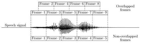
Figure 1.
Illustration of framing performed on a time-sampled speech signal to obtain overlapped and non-overlapped frames for analysis. The signal waveform of this illustration represents a speech utterance ‘seven’ from a recorded file ‘06f6c194_nohash_1.wav’ of the Speech Commands dataset [1].
The resulting frames have a fixed duration , chosen appropriately based on signal analysis. For instance, the wide-band spectrogram analysis requires frames of shorter duration (e.g., ms) to achieve good time resolution. In contrast, the narrow-band spectrogram analysis requires frames of relatively longer duration (e.g., ms) to achieve good frequency resolution [2]. Furthermore, in the case of overlapped framing, the adjacent frames are overlapped by to smooth the transition from one frame to another. In speech and audio processing, framing is typically performed after pre-emphasis1 and before windowing2.
1.2. Related Works
In recent years, a wide variety of framing hardware architectures (FHA) were disclosed in the literature [3,4,5,6,7,8,9] for applications employing digital speech and audio systems. These FHAs primarily comprise memory unit(s), wherein the memory width is equal to the speech or audio sample word size (say n bits); the total no. of memory locations (say M) depends on the desired frame size (); and the coordination of memory units is based on the desired frame overlap size () (or the percentage of frame overlap ()). Furthermore, the existing FHAs [3,4,5,6,7,8,9] broadly fall under two distinct categories, viz., blocking [3,4,5,6,7,8] and non-blocking [9]. The blocking type FHAs [3,4,5,6,7,8] use memory unit(s), wherein the total no. of memory locations is equal to the desired frame size (i.e., ). Therefore, they divide the signal samples into discrete frames by buffering them in the memory unit(s). In contrast, the non-blocking type FHAs [9] use memory unit(s), wherein the total no. of memory locations is less than the desired frame size (i.e., ). Therefore, they divide the signal samples into discrete frames without buffering them in the memory unit(s).
The high-level architectures of the state-of-the-art blocking type framing hardware in [3,4,5,6,7,8] are illustrated in Figure 2. The FHA in [3] (see Figure 2a) uses a 252-by-16 (depth-by-width) dual-port (DP) random access memory (RAM). It is divided into three fixed and equi-sized partitions (say and ) to obtain frames (of ms duration having samples) overlapped by (equivalent to ms duration with samples) from speech signals sampled with a frequency of kHz. The FHA in [4] (see Figure 2b) uses a P-by-16 auxiliary RAM (A-RAM). It is divided into two fixed and equi-sized partitions (say and ) to obtain frames (of ms duration having P samples, where ) overlapped by (equivalent to ms duration with samples) from speech signals sampled with a frequency of kHz. The FHA in [5] (see Figure 2c) uses two (double) 256-by-16 buffers to obtain frames (of ms duration having samples) overlapped by (equivalent to ms duration with samples) from speech signals sampled with a frequency of kHz. The FHA in [6] (see Figure 2c) uses two (double) 128-by-16 buffers to obtain frames (of ms duration having samples) overlapped by (equivalent to ms duration with samples) from speech signals sampled with a frequency of kHz. The FHA in [7,8] (see Figure 2d) uses a 200-by-16 DP-RAM. It is divided into two fixed and equi-sized partitions (say and ) to obtain frames (of ms duration having samples) overlapped by (equivalent to ms duration with samples) from music (audio) signals sampled with a frequency of kHz.
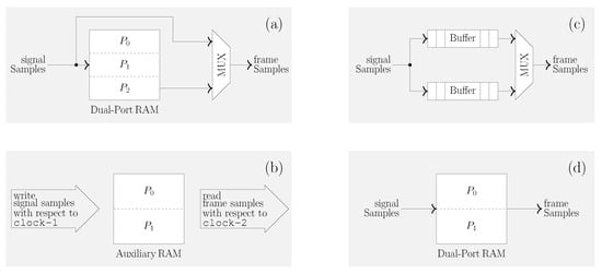
Figure 2.
High-level architectures of the state-of-the-art blocking type framing hardware in the literature. (a) FHA in [3]. (b) FHA in [4]. (c) FHA in [5,6]. (d) FHA in [7,8]. Refer to Appendix A for brief descriptions outlining the functionality of these FHAs.
The high-level architectures of the state-of-the-art non-blocking type framing hardware in [9] are illustrated in Figure 3. In [9], two FHAs (say I and II) were disclosed. The FHA-I in [9] (see Figure 3a) uses a 128-by-16 RAM-based shift register (SR) to obtain frames (of ms duration having samples) overlapped by (equivalent to ms duration with samples) from speech signals sampled with a frequency of kHz. Similarly, the FHA-II in [9] (see Figure 3b) uses three 64-by-16 RAM-SRs to obtain frames (of ms duration having samples) overlapped by (equivalent to ms duration with samples) from speech signals sampled with a frequency of kHz. The FHAs-I and -II in [9] support continuous-flow operation to process streaming or stored speech signals at high-speed.
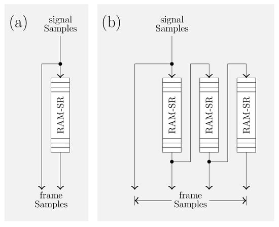
Figure 3.
High-level architectures of the state-of-the-art non-blocking type framing hardware in the literature. (a) FHA-I in [9]. (b) FHA-II in [9]. Refer to Appendix B for brief descriptions outlining the functionality of these FHAs.
The key aspects of blocking and non-blocking type FHAs, as discussed, are tabulated in Table 1 for quick reference.

Table 1.
Comprehensive review of the state-of-the-art blocking and non-blocking type FHAs in the literature.
1.3. Problem Statement
The FHAs in [3,4,5,6,7,8,9] operate on speech or audio samples of specific word size and output frames of specific frame size and frame overlap size (and percentage of frame overlap), as demanded by a specific application. However, speech and audio applications often require framing signal samples of varied word sizes with varied frame sizes and frame overlap sizes (and percentage of frame overlap). Therefore, the existing FHAs must be redesigned appropriately to keep up with the variability in word size, frame size and frame overlap size (and percentage of frame overlap), as demanded across multiple applications. Redesigning the existing FHAs for each specific application can be tedious to the hardware designers as it necessitates manual intervention at the register-transfer level (RTL). This involves making adjustments or modifications to the base architectures, which is often time-consuming due to extended development cycles that include design and verification processes. The optimal solution to overcome the problem of redesigning the existing FHAs for each specific application lies in transforming their base architectures into soft, ready-to-use and configurable intellectual property (IP) cores3 that allow the end users to customize the required hardware as per the application requirements.
However, the base architectures of existing framing hardware are inappropriate for the IP core design due to the following limitations:
- Limited adaptability to accommodate variability in frame size (): The base architectures of framing hardware in [4,5,6,7,8] and [9]-I, [3] and [9]-II are adaptable to specific frame sizes that are integral multiples of 2, 3 and 4, respectively. Therefore, their adaptability does not extend to some arbitrary frame sizes required by specific applications, e.g., consider a speech recognition application, wherein kHz and ms [10]. In this case, samples (i.e., ). Here, 253 is not an integral multiple of 2, 3 and 4, and 297 is not an integral multiple of 2 and 4.
- Non-adaptable to accommodate variability in frame overlap size () (and percentage of frame overlap): The base architectures of framing hardware in [4,5,6,7,8] and [9]-I, [3] and [9]-II output frames that are overlapped by , and , respectively, by default, due to the specific hardware configuration (e.g., double buffers [5,6] and triple RAM-SRs [9]-II). Therefore, they are not adaptable to some arbitrary percentages of frame overlap required by specific applications, e.g., consider a speech recognition application, wherein samples and samples [10]. In this case, (i.e., ).
Therefore, it becomes apparent that if the IP core(s) is (are) developed using the base architectures of existing framing hardware, then it (they) offer(s) a limited degree of customization, wherein the word size is customizable as desired; the frame size () is customizable to a certain extent; and the frame overlap size () (and the percentage of frame overlap) remains unchanged.
Furthermore, the base architectures of existing framing hardware, particularly in [3,4,7,8], are inappropriate for the IP core design due to the following drawbacks:
- The FHAs in [3,4,7,8] tend to have an increased area cost and power consumption due to using multi-port memory units.
- The FHA in [4] employs a dual clocking scheme, wherein its A-RAM unit operates with two distinct clocks, in contrast to other FHAs (and the typical digital speech and audio systems, e.g., in [7,8,11,12]) that operate solely with a single clock. The dual clocking scheme necessitates using additional functional units comprising: a clock signal generator for deriving two clock signals; a reset signal generator for providing reset signals to the functional units operating in two clock domains; and multiple clock domain crossing (CDC) units for enabling the required signals to cross between two clock domains. Consequently, this architecture incurs an additional area cost and power consumption when compared to the FHAs in [3,7,8].
The limitations and drawbacks, as discussed, make the existing FHAs inappropriate for the IP core design. Therefore, speech and audio applications require a frame blocking IP core based on a versatile base architecture that can be configured to operate on speech or audio samples of any specific word size and output frames with any specific frame size and frame overlap size (and percentage of frame overlap). To the best of our knowledge, to date, no such IP core exists in the literature, and the requirement for the same is still outstanding.
The research work reported in this article specifically focuses on addressing the mentioned requirement, primarily within the realm of speech applications, while being applicable to audio (non-speech) applications as well. The significant contributions made in this article are listed as follows:
- First, a novel blocking type FHA, capable of accommodating variability in word size, frame size and frame overlap size (and percentage of frame overlap) is proposed.
- Second, the proposed FHA is transformed into a field-programmable gate array (FPGA)-based soft, ready-to-use and configurable frame blocking IP core using the Xilinx® Vivado™ tool.
1.4. Brief Summary and Article Organization
In summary, the FHAs in the literature support framing speech or audio samples of specific word size with specific frame size and frame overlap size. However, speech and audio applications often require framing signal samples of varied word sizes with varied frame sizes and frame overlap sizes. Therefore, the existing FHAs must be redesigned appropriately to keep up with the variability in word size, frame size and frame overlap size, as demanded across multiple applications. Redesigning the existing FHAs for each specific application is laborious, prompting the need for a configurable IP core. The existing FHAs are inappropriate for creating configurable IP cores as they lack adaptability to accommodate variability in frame size and frame overlap size. Therefore, to address these issues, a novel FHA, adaptable to accommodate the desired variability, is proposed. Furthermore, the proposed FHA is transformed into an FPGA-based soft IP core using the Xilinx® Vivado™ tool. The resulting IP core offers a ready-to-use and configurable solution for frame blocking, catering to the dynamic needs of numerous applications incorporating real-time digital speech and audio systems.
2. Methodology
In this article, we propose a novel blocking type FHA that uses an M-by-n single-port (SP) RAM (having no fixed partitions) to output frames, characterized by: a default frame size (i.e., samples) or any other specific frame size (i.e., samples); and a specific frame overlap size (i.e., samples, such that ), from speech signals sampled with a wide range of sampling frequency. The methodology adopted by our FHA to perform framing involves two distinct phases of operations on SP-RAM, viz., a memory write phase and a memory read phase, as illustrated in Figure 4. The memory write phase involves operations to write (store) speech samples in SP-RAM to realize a frame. Conversely, the memory read phase involves operations to read (output) the realized frame samples from SP-RAM. Therefore, the FHA performs framing by alternating between the memory write and read phases, explained in detail, using a timing diagram illustrated in Figure 5, as follows:

Figure 4.
Methodology of our proposed FHA for framing time-sampled digital speech signals.
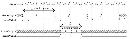
Figure 5.
Timing diagram illustrating the framing methodology of our proposed FHA. The signals clock, dataSample and dataValid denote the inputs and frameSample and frameValid denote the outputs of the FHA. The dataValid input is asserted for one clock cycle, equivalent to ns, at every instant when a speech sample arrives (for every ms, equivalent to clock cycles) at the dataSample input. The frameValid output is asserted (for ns, equivalent to clock cycles) at every instant when the FHA outputs a frame of samples, consecutively (in clock cycles), via the frameSample output.
2.1. Memory Write Phase
Let the FHA operate at a clock frequency of MHz (clock period of ns). Consider an active data source (e.g., an analog-to-digital (A2D) converter) that transmits speech samples to the FHA with a sampling frequency of kHz (sampling period of ms). Therefore, the FHA receives a speech sample (say at the dataSample input) for every ms, equivalent to clock cycles, as illustrated in Figure 5, where
and the effect of and on is illustrated graphically in Figure 6a. The received samples are consecutively stored in SP-RAM.
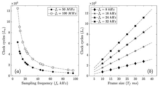
Figure 6.
(a) Effect of and on . For a fixed (or ), decreases exponentially with an increase in (or decrease in ). For a fixed , increases with an increase in . (b) Effect of and on . For a fixed , increases with an increase in (or decrease in ). For a fixed (or ), increases with an increase in (or ).
2.2. Memory Read Phase
The FHA reads and outputs the stored samples from SP-RAM (say via a frameSample output) in proper order with a frequency of MHz, at specific instants, when the mentioned samples collectively represent a valid frame. Therefore, the FHA takes ns, equivalent to clock cycles, to output an entire frame, as illustrated in Figure 5, where
and the effect of and on is illustrated graphically in Figure 6b.
2.3. Framing Mechanism
The framing mechanism of our proposed FHA is briefly summarized as follows: For the first frame, the FHA writes (stores) a series of samples consecutively in SP-RAM and reads (outputs) them consecutively in the same order. Conversely, for every subsequent frame, the FHA writes a series of samples consecutively in SP-RAM and reads a series of samples consecutively in the proper order. The FHA outputs successive frames for every ms, equivalent to clock cycles, as illustrated in Figure 7, where
and the effect of (or ) and (or ) on is illustrated graphically in Figure 8.
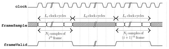
Figure 7.
Timing diagram illustrating a scenario, wherein our proposed FHA outputs the successive frames (for every ms, equivalent to clock cycles).
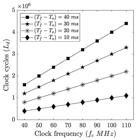
Figure 8.
Effect of (or ) and (or ) on . In this graphical illustration, we consider ms and ms such that , respectively. For a fixed (or ), increases with an increase in . For a fixed , increases with an increase in (or decrease in ).
2.4. Theoretical Condition(s) for Proper Framing
As our proposed FHA utilizes SP-RAM, it is crucial for the FHA to efficiently alternate between the memory write and read phases of the framing mechanism. Specifically, the transition from the memory read phase to the memory write phase must complete before a speech sample arrives at the dataSample input for ensuring successful reception and storage in SP-RAM. Therefore, the theoretical condition(s) for our FHA to perform proper framing is (are) deduced from (1) and (2) as,
We solve (4) for by considering MHz (a common target clock frequency range for speech-based applications, e.g., [13]) and , where kHz (a common target sampling frequency range for speech and audio applications). Further, we apply a constraint, ms. Finally, the obtained solutions are graphically illustrated in Figure 9, which primarily depicts the range (marked as a shaded region) supported by our FHA for specific and . Let such that kHz, where kHz and is denoted by a vertical dotted line in Figure 9. It is evident that , our FHA supports framing ms. Further, range increases when increases with . Furthermore, the supported range decreases .
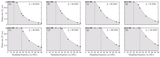
Figure 9.
Solutions of (4), i.e., ; MHz, kHz and ms. The sub-figures (a–h) illustrate the solutions of as increases from 40–110 MHz with a step size of 10 MHz. The dashed line denotes ; the shaded region denotes ; and the vertical dotted line denotes kHz.
3. Proposed FHA and Frame Blocking IP Core
3.1. Architecture
The proposed blocking type FHA is illustrated in Figure 10. It comprises: a four-state algorithmic state machine with datapath (ASMD)-based controller; an M-by-n SP-RAM with synchronous read and write enable configuration; and a 2-to-1 MUX. The ASMD is the core of the framing hardware and is responsible to perform framing using SP-RAM according to the methodology discussed in Section 2. The MUX multiplexes the necessary write and read addresses generated by the ASMD to the common address input of SP-RAM during memory write and read phases of the framing mechanism, respectively.
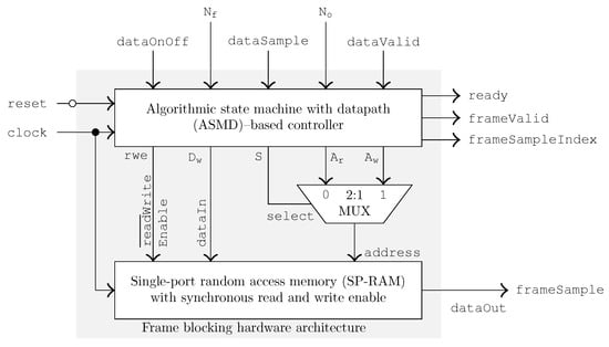
Figure 10.
Proposed blocking type FHA [14]. In addition to the ASMD, MUX and SP-RAM, the FHA uses delay units (not shown in the figure) specifically on the frameValid and frameSampleIndex outputs to synchronize them with the frameSample output.
The input and output (I/O) ports of our FHA are listed and briefly described in Table 2. Furthermore, the control, data and address output ports and internal control logic registers (apart from those that particularly drive the output ports) of the ASMD are listed and briefly described in Table 3 and Table 4, respectively.
Table 2.
I/O ports of our FHA.
Table 3.
Control, data and address output ports of the ASMD.
Table 4.
Internal control logic registers of the ASMD.
The ASMD is realized with four states, viz., , , and , using the design methodology presented in [15], and its state diagram is illustrated in Figure 11. The state is the idle state. The state handles operations of the memory write phase to realize a frame in SP-RAM. The state handles operations that control switching between the memory write and read phases of the framing mechanism. The state handles operations of the memory read phase to output the realized frame samples from SP-RAM.
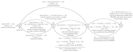
Figure 11.
State diagram of the ASMD-based controller used in our proposed blocking type FHA. In this state diagram, the conditions for state transitions and key outputs during state transitions are symbolically represented near arcs. The horizontal line separates the two condition-output pairs. Refer to Section 3.3 for a detailed functional description of this state diagram.
3.2. Brief Functional Description
The ASMD’s functionality is described in brief as follows: Upon power-up, the ASMD switches to the state by default. It remains in the state indefinitely and switches to the state when the data source becomes active.
- Case-1:
While in the state, the ASMD waits for nearly ms (provided that the data source is active) to receive a speech sample. Upon receiving a speech sample, the ASMD switches to the state to store it in SP-RAM. Furthermore, the ASMD checks if the samples in SP-RAM collectively represent a valid frame. If the samples in SP-RAM do not represent a valid frame, then the ASMD switches back to the state to receive a subsequent speech sample. The switching activity between and states continues to realize a frame in SP-RAM. Conversely, if the samples in SP-RAM collectively represent a valid frame, then the ASMD switches to the state to output the realized frame samples from SP-RAM. While in the state, the ASMD outputs each frame sample with a time period of ns. Therefore, the ASMD remains in the state for ns to output entire frame samples and subsequently switches to the state to check the status of the data source. If the data source is inactive, then the ASMD stops framing and switches to the state. Conversely, if the data source is active, then the ASMD switches to the state and continues to perform framing, as discussed.
- Case-2:
While in the state, at any instance, if the data source becomes inactive, then the ASMD no longer waits for ms as the speech samples cease to arrive from the data source. Furthermore, the ASMD checks if the last frame is partly realized in SP-RAM. If the last frame is not partly realized in SP-RAM, then the ASMD stops framing and switches to the state. Conversely, if the last frame is partly realized in SP-RAM, then the ASMD generates a zero-magnitude sample (to pad the last frame) and switches to the state to store it in SP-RAM. Furthermore, the ASMD checks if the samples in SP-RAM collectively represent a valid last frame. If the samples in SP-RAM do not represent a valid last frame, then the ASMD switches back to the state to generate a subsequent zero-magnitude sample. The switching activity between and states continues to pad the last frame in SP-RAM with the required no. of zero-magnitude samples. Conversely, if the samples in SP-RAM collectively represent a valid last frame, then the ASMD switches to the state to output the realized zero-padded last frame samples from SP-RAM. While in the state, the ASMD outputs the last frame samples (in the similar manner, as discussed) and subsequently switches to the state to check the status of the data source. As the data source is inactive at this instant, the ASMD stops framing and switches to the state.
3.3. Detailed Functional Description
The ASMD’s functionality is described in detail with reference to its state diagram, illustrated in Figure 11, and the algorithmic state machine (ASM) charts of its four states, viz., , , and , illustrated in Figure 12, Figure 13, Figure 14 and Figure 15, respectively, as follows:
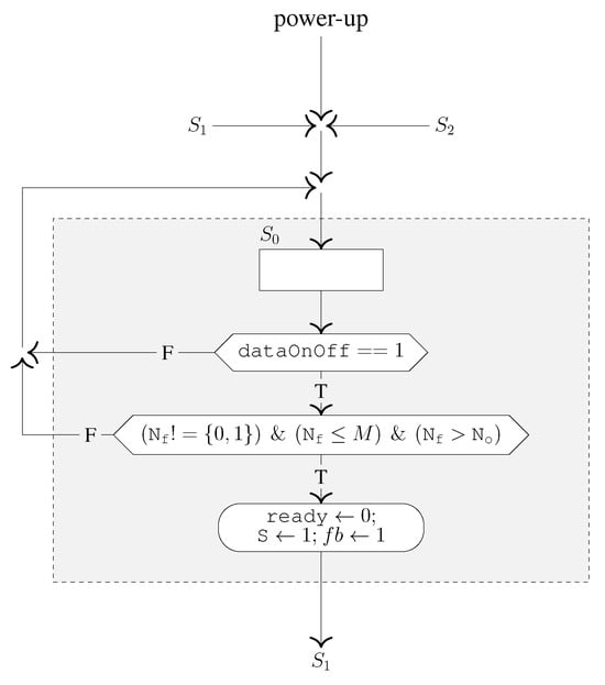
Figure 12.
ASM chart of the state.
- state:
The ASMD switches to the state by default on power-up or from or states on completion of framing. It remains in the state for an indefinite no. of clock cycles until it is initiated by the data source via the dataOnOff input. Therefore, it monitors the dataOnOff input and accordingly performs operations categorized as follows:
- (a)
- When dataOnOff = 0, it signifies that the data source is inactive and the speech signal is not available for framing. Therefore, the ASMD waits in the state.
- (b)
- When dataOnOff = 1, it signifies that the data source is active and the speech signal is available for framing. Therefore, the ASMD makes the state transition to start framing (provided that the configuration data () of Nf input satisfies the following conditions: , and ) and accordingly updates its registers and generates outputs as follows:
- (i)
- The ready output is reset to a low logic to denote the hardware status as busy.
- (ii)
- The S output is set to a high logic that enables the MUX to multiplex the Aw output to the address input of SP-RAM during the memory write operations.
- (iii)
- The register is set to a high logic that enables the ASMD to realize the first frame in SP-RAM.

Figure 13.
ASM chart of the state.
Figure 13.
ASM chart of the state.

- state:
Upon switching, the ASMD remains in the state for at most clock cycles (equivalent to ms) when dataOnOff = 1 or for one clock cycle when dataOnOff = 0, and performs operations categorized as follows:
- (a)
- When dataOnOff = 1 and dataValid = 0, it signifies that a valid sample of the speech signal is not available at the dataSample input and is yet to arrive from the data source. Therefore, the ASMD waits in the state for the sample arrival.
- (b)
- When dataOnOff = 1 and dataValid = 1, it signifies that a valid sample of the speech signal has arrived at the dataSample input. Therefore, the ASMD makes the state transition to write (store) the received sample in SP-RAM and accordingly updates its registers and generates outputs as follows:
- (i)
- The received sample of the speech signal is made available at the Dw output.
- (ii)
- The address to write (store) the sample of Dw output in SP-RAM is computed (using a generalized conditional expression) as,where denotes a write address register that drives the Aw output.
- (iii)
- The rwe output is set to a high logic to enable memory write operation on SP-RAM.
- (iv)
- The register is incremented by one as the received sample of the speech signal is stored in SP-RAM.
- (c)
- When dataOnOff = 0, it signifies that the data source is inactive and has stopped transmitting speech samples to the dataSample input, and at the same instant, a new frame realization is yet to begin. Therefore, the ASMD makes the state transition to stop framing and accordingly updates its registers and generates the following outputs:
- (i)
- The ready output is set to a high logic to denote the hardware status as idle and ready to start framing on the subsequent speech signal.
- (ii)
- The S output is reset to a low logic, i.e., the default condition.
- (d)
- When dataOnOff = 0 and Cw ≠ 0, it signifies that the data source is inactive and has stopped transmitting speech samples to the dataSample input, and at the same instant, a new frame realization is already under progress, during which a frame, referred to as the last frame, is partly realized in SP-RAM. Therefore, the ASMD performs zero-padding to the last frame to realize it completely. In this regard, the ASMD makes the state transition to write (store) a zero-magnitude sample in SP-RAM and accordingly updates its registers and generates outputs as follows:
- (i)
- The zero-magnitude sample is made available at the Dw output.
- (ii)
- The address to write (store) the sample of Dw output in SP-RAM is computed appropriately using (5).
- (iii)
- The rwe output is set to a high logic to enable memory write operation on SP-RAM.
- (iv)
- The register is incremented by one as the zero-magnitude sample is stored in SP-RAM.

Figure 14.
ASM chart of the state.
Figure 14.
ASM chart of the state.

- state:
The ASMD switches to the state from the state, after initiating a memory write operation, or from the state, after completing the memory read operations. It stays in the state for one clock cycle and performs operations categorized with respect to the register (that drives the rwe output), as follows:
- (A)
- When , it signifies that the ASMD has switched from the state, and a sample determined by the Dw output is stored in SP-RAM at an address determined by the Aw output. Subsequently, the ASMD initiates to reset the rwe output to a low logic to disable memory write on SP-RAM and makes either the or the state transition to continue frame realization or read (output) the realized frame samples from SP-RAM, respectively. The ASMD makes the relevant state transition, defined as follows:
- (a)
- When , it signifies that the first frame is partly realized in SP-RAM. Therefore, the ASMD makes the state transition.
- (b)
- When , it signifies that the first frame is fully realized in SP-RAM. Therefore, the ASMD makes the state transition and accordingly updates its registers and combinational logic and generates outputs as follows:
- (i)
- The register is reset to a low logic that enables the ASMD to realize subsequent frame(s) (other than the first frame) in SP-RAM.
- (ii)
- The register is reset to zero, which enables the counter to newly count the subsequent write operations performed on SP-RAM to realize the subsequent frame.
- (iii)
- The S output is reset to a low logic that enables the MUX to multiplex the Ar output to the address input of SP-RAM during the memory read operations.
- (iv)
- The address to read (output) the starting sample of the first frame from SP-RAM is initialized in a register, say (that drives the Ar output), by resetting it to zero.
- (v)
- A combinational logic, denoted as , is used as an offset to compute the (read) address corresponding to the starting sample of every frame being realized in SP-RAM. It is initialized by resetting it to zero.
- (c)
- When , it signifies that a frame (other than the first frame) is partly realized in SP-RAM. Therefore, the ASMD makes the state transition.
- (d)
- When , it signifies that a frame (other than the first frame) is fully realized in SP-RAM. Therefore, the ASMD makes the state transition and accordingly updates its registers and generates an output as follows:
- (i)
- The register is reset to zero, which enables the counter to newly count the subsequent write operations performed on SP-RAM to realize the subsequent frame.
- (ii)
- The S output is reset to a low logic that enables the MUX to multiplex the Ar output to the address input of SP-RAM during the memory read operations.
- (B)
- When , it signifies that the ASMD has switched from the state. Subsequently, the ASMD performs operations categorized as follows:
- (a)
- When dataOnOff = 1, it signifies that the data source is active. Therefore, the ASMD makes the state transition to continue framing and accordingly updates its register and generates an output as follows:
- (i)
- The S output is set to a high logic that enables the MUX to multiplex the Aw output to the address input of SP-RAM during the memory write operations.
- (b)
- When dataOnOff = 0, it signifies that the data source is inactive and has stopped transmitting speech samples to the dataSample input. Therefore, the ASMD makes the state transition to stop framing and accordingly updates its register and generates an output as follows:
- (i)
- The ready output is set to a high logic to denote the hardware status as idle and ready to start framing on the subsequent speech signal.

Figure 15.
ASM chart of the state. In this ASM chart, denotes the sign bit.
Figure 15.
ASM chart of the state. In this ASM chart, denotes the sign bit.

- state:
Upon switching, the ASMD remains in the state for clock cycles (equivalent to ns) and performs operations categorized as follows:
- (a)
- When , it signifies that the realized frame samples are yet to be read from SP-RAM. Therefore, the ASMD initiates to read (output) the first sample of the realized frame from SP-RAM (at an address determined by the Ar output) and accordingly updates its registers and generates an output as follows:
- (i)
- The register is incremented by one as the first sample of the realized frame is read from SP-RAM.
- (ii)
- The frameValid output is set to a high logic as the hardware begins to output the realized frame samples, consecutively, via the frameSample output.
- (b)
- When , it signifies that the realized frame samples are partly read from SP-RAM. Therefore, the ASMD initiates to read (output) a jth sample (such that ) of the realized frame from SP-RAM and accordingly updates its registers and generates an output as follows:
- (i)
- The address to read (output) the jth sample of the realized frame from SP-RAM is computed as,
- (ii)
- The register is incremented by one as the jth sample of the realized frame is read from SP-RAM.
- (c)
- When , it signifies that the realized frame samples are fully read from SP-RAM. Therefore, the ASMD makes the state transition and accordingly updates its registers and combinational logic and generates outputs as follows:
- (i)
- The register is reset to zero, which enables the counter to newly count the subsequent read operations performed on SP-RAM to output the subsequent frame upon realization.
- (ii)
- The frameValid output is reset to a low logic as the hardware has finished outputting the realized frame samples via the frameSample output.
- (iii)
- The (read) address corresponding to the starting sample of the subsequent frame is pre-computed as,where . The expression () denotes . It ensures that the read addresses are generated within the range .
For a more comprehensive understanding of the functionality, refer to supplementary materials, specifically Figure S1 (Part-1–3), which correspond to the behavioral simulation of our FHA (illustrating the signal timing waveforms captured during a framing task performed on a short finite-length test sequence) discussed in detail in Section S1 of Document S1. These visual aids offer valuable insights into the real-time behavior of our FHA, enhancing the clarity and depth of the presented information.
3.4. Practical Condition(s) for Proper Framing
Let the dataOnOff input of our FHA be at a high logic and the ASMD perform framing on speech samples according to the methodology discussed in Section 2. Consider a framing scenario, wherein the ASMD makes a series of state transitions to switch from the memory write phase to the memory read phase and subsequently switch back to the memory write phase, represented symbolically as,
From (8), it is evident that the ASMD takes (where ) clock cycles to exit from and re-enter into the state. Furthermore, the ASMD must re-enter into the state before a speech sample arrives at the dataSample input to ensure successful reception and storage in SP-RAM. Therefore, the practical condition(s) for our FHA to perform proper framing is (are) deduced as,
3.5. FHA Design and Functional Verification
We used the Xilinx® Vivado™ 2021.1 [16] tool to design and simulate our proposed FHA and to create, package, implement and test our proposed frame blocking IP core. The RTL design of our FHA is carried out using Verilog-HDL [17]. The HDL descriptions are parameterized, making them ideal for creating the configurable frame blocking IP core.
Before creating the desired frame blocking IP core, the HDL descriptions of our FHA are thoroughly verified for functionality through extensive behavioral simulations using Verilog testbenches. The simulations are performed using random test sequences and speech signals (that are diverse in terms of the sampling frequency () and the sample word size (n)) sourced from recordings of multiple speech databases, as listed in Table A1 (refer to Appendix C). Refer to supplementary materials, specifically Section S1 of Document S1, for more details regarding an example behavioral simulation performed to verify the functionality of our FHA.
3.6. Frame Blocking IP Core Creation and Packaging
We created and packaged [18] our proposed frame blocking IP core using the parameterized RTL descriptions of our FHA. The resulting IP core, along with its customization menu, is illustrated in Figure 16. The customization menu offers end users a range of IP customization options, categorized as ‘General Options’ and ‘Optional–Input and –Outputs’. The ‘General Options’ category contains two configurable parameters , viz., ‘Word Size’ and ‘Frame Size (default)’, wherein the end user must configure the former and latter with the desired values, denoting the word size of speech samples (within the range bits) and the frame size (say , within the range samples that satisfies (9) for specific and ), respectively, as per the application requirements.
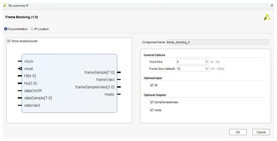
Figure 16.
Proposed frame blocking IP core, created and packaged using the Xilinx® Vivado™ 2021.1.
The ‘Optional Input’ category defines the IP input Nf as optional. This input is enabled by default, and the end user may disable it if needed. If the Nf input is enabled, then the IP core is capable of realizing frames with any specific frame size, i.e., samples, as determined by the Nf input. Conversely, if the Nf input is disabled, then the IP core realizes frames with default frame size, i.e., samples. Similarly, the ‘Optional Outputs’ category defines the two IP outputs, viz., frameSampleIndex and ready, as optional. These outputs are enabled by default, and the end user may disable them if needed.
Furthermore, if the optional I/Os are partly or fully disabled, then the FHA resulting from the IP customization uses an adapted variant of the ASMD, wherein
- the logic associated in connecting the register to the frameSampleIndex output is trimmed, when the frameSampleIndex output is disabled.
The proposed IP core is compatible for implementation with most of the Xilinx®-based FPGA targets, including devices from the 7-series product families [19]. We have implemented our IP core on multiple FPGA targets, viz., Basys 3 [20] and ZedBoard™ [21], and thoroughly tested and validated its functionality using multiple test cases. Refer to supplementary materials, specifically Section S2 of Document S1, for more details regarding an example implementation of our IP core on an FPGA target to test and validate its functionality. Additionally, refer to Video S1 for a comprehensive demonstration of testing and validation of our IP core’s functionality on an FPGA target.
4. Results and Discussions
4.1. Implementation Results
We performed multiple implementations of our proposed frame blocking IP core (based on multiple combinations of the configuration parameters, viz., n and M) on an FPGA target, specifically the Avnet® ZedBoard™ [21] having the xc7z020clg484-1 device from the Xilinx® Zynq™ 7000 APSoC (all programmable system-on-chip) family [22]. The results, covering multiple hardware-related aspects, viz., maximum supported clock frequency (speed), resource utilization on the FPGA fabric (area) and total on-chip power consumption, for each specific implementation of our IP core, are reported in Table 5.
Table 5.
Summary of resource utilization, total on-chip power consumption and maximum supported clock frequency for multiple implementations of our proposed frame blocking IP core on the Xilinx® Zynq™ xc7z020clg484-1 FPGA.
In Table 5, for each specific implementation of our IP core that operates at a target clock period of ns, the maximum clock frequency supported by the target device speed grade is estimated as [23],
where denotes the worst negative slack of the target clock period . The estimates from Table 5 confirm that our IP core can effectively operate at a target clock frequency ranging up to 110 MHz (and beyond to a certain extent) making it well-suited for the majority of speech-based applications, e.g., [13].
The resource utilization by our IP core (e.g., slice, slice look-up tables (LUT), slice registers, block RAM (BRAM), etc.) on an FPGA fabric varies with IP configuration , as reported in Table 5. Furthermore, our IP core keeps the overall resource utilization at a minimum as it realizes the required SP-RAM using BRAM resources on the FPGA fabric. The total memory utilization () by our IP core using BRAM resources of FPGA varies with IP configuration as,
where (samples) denotes the default frame size, and the effect of M and n on is illustrated graphically in Figure 17.
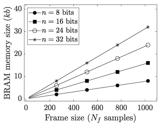
Figure 17.
Total memory utilization by our proposed frame blocking IP core using BRAM resources on FPGA. For a fixed M (or ), increases with an increase in n. For a fixed n, increases with an increase in M (or ).
The total on-chip power consumption by our IP core depends on multiple factors, viz., IP configuration (n, M), clock frequency (), FPGA target device, etc. The power analysis estimates of our IP core for a variable IP configuration, under a fixed clock frequency and target device, as reported in Table 5, show that the total on-chip power consumption varies within the range mW.
4.2. Comparison with Baselines
A comprehensive comparison between our proposed frame blocking IP core and the FHA baselines is presented in Table 6, and the key inferences drawn from this table are summarized as follows:
Table 6.
Comprehensive comparison between our proposed frame blocking IP core and the FHA baselines.
- The IP core is based on a blocking type FHA. It has a dynamic hardware configuration that varies with IP customization when compared to the blocking [3,4,5,6,7,8] and non-blocking [9] type FHA baselines having a fixed hardware configuration.
- The FHA baselines [3,4,5,6,7,8,9] use memory unit(s) (viz., DP-RAM with three fixed partitions [3], A-RAM with two fixed partitions [4], double buffers [5,6], DP-RAM with two fixed partitions [7,8] and RAM-SR(s) [9]), wherein the memory width is fixed to bits [3,4,5,6,7,8,9], and the total no. of memory locations (M) is fixed to 252 [3], P (where ) [4], 512 [5], 256 [6], 200 [7,8], 128 [9]-I and 192 [9]-II. Therefore, they perform framing on speech (or audio) samples having a word size of bits and output frames having a fixed frame size ( samples, ms), viz., (252, 22.8) [3], (P, 10) [4], (512, 32) [5], (256, 16) [6,9] and (200, 20) [7,8]. Conversely, our IP core uses a memory unit (SP-RAM with no fixed partitions), wherein the memory width can be customized according to the speech sample word size (n) within the range , and the total no. of memory locations (M) can be customized according to the desired frame size () (that satisfies (9) for specific and ) within the range .
- The IP core can vary frame size within the range via the Nf input (provided that it is enabled during IP customization) and frame overlap size within the range via the No input.
- This feature is not available in the FHA baselines [3,4,5,6,7,8,9]. Therefore, they perform framing with fixed frame size, as discussed, and frame overlap size ( samples, ms), viz., (168, 15.2) [3], (, 5) where [4], (256, 16) [5], (128, 8) [6] and [9]-I, (100, 10) [7,8] and (192, 12) [9]-II.
- The IP core supports overlapped framing () and non-overlapped framing (for ), as determined by the No input, whereas the FHA baselines [3,4,5,6,7,8,9] exclusively support overlapped framing.
- The IP core can vary the percentage of frame overlap (i.e., ) within the range [0, ]·100% via the No input.
- This feature is not available in the FHA baselines [3,4,5,6,7,8,9]. Therefore, they perform framing with a fixed percentage of frame overlap, viz., [3], [4,5,6,7,8] and [9]-I and [9]-II.
- The IP core supports zero-padding, specifically performed to the last frame when it falls short of speech samples. However, whether the FHA baselines [3,4,5,6,7,8,9] accommodate this feature remains unknown.
- The IP core supports framing speech signals (with desired frame size, ms) sampled with a frequency, kHz, when operated at a clock frequency, MHz, where kHz, for MHz; kHz, for MHz; kHz, for MHz; and kHz, for MHz (see Figure 9). Conversely, the FHA baselines [3,4,5,6,7,8] perform framing on speech (or audio) signals sampled with a specific frequency , viz., kHz [3], 16 kHz [5,6], 10 kHz [7,8] or a finite set of , viz., kHz [4]. However, the extent to which the FHA baselines [3,4,5,6,7,8] can effectively support the framing of speech (or audio) signals sampled with a wide range of remains unknown.
- The IP core is versatile, offering configurability for framing in applications based on narrow- and wide-band spectrogram analysis of speech and audio, in contrast to the FHA baselines [3,4,5,6,7,8,9], exclusively designed for applications based on narrow-band spectrogram analysis of speech and audio.
Table 6 presents a comprehensive comparison between our proposed frame blocking IP core and the FHA baselines, specifically focusing on multiple generalized aspects related to framing and hardware. Notably, certain important hardware-related aspects, viz., maximum supported clock frequency (speed), resource utilization on the FPGA fabric (area) and total on-chip power consumption, were not included in this comparison. This omission arises because although we can explicitly report estimates for the speed, area and power of our IP core, comparable estimates for the FHA baselines are not explicitly reported in the literature. Instead, these estimates are typically reported for speech (and audio) systems, with FHA serving as a subsystem among several others. Therefore, the speed, area and power estimates for the FHA baselines are not readily accessible. Moreover, if the speed, area and power estimates for the FHA baselines are readily accessible, then their comparisons with the equivalent estimates of our IP core would still be inappropriate as the implementations of our IP core and the FHA baselines were performed across a wide range of FPGA target devices from different manufactures and families, as reported in Table 6, wherein the configuration of basic blocks, e.g., LUTs, within these devices varies significantly.
Given these challenges, the most viable approach to make a more detailed comparison would involve obtaining the speed, area and power estimates for the FHA baselines based on their implementations performed on a common FPGA target, specifically the one used to report the equivalent estimates for our IP core. Consequently, to advance in this endeavor, we replicated the FHA baselines (through RTL design using Verilog HDL in the Xilinx® Vivado™ tool) by taking into account the following key considerations:
- Blocking type FHA baselines [3,4,5,6,7,8]:
- Their I/O configuration matches that of our IP core, except for the Nf and No inputs.
- They perform framing similar to the methodology discussed in Section 2 (refer to Section 2.1, Section 2.2, Section 2.3).
- They independently perform operations of memory write and read phases of the framing mechanism using two dedicated controllers.
- The FHA baseline [3] is slightly modified by eliminating the use of the MUX. This simplification ensures consistency with the framing mechanism (refer to Section 2.3) adopted by other FHA baselines [4,5,6,7,8], as well as by our IP core.
- The FHA baseline [4] requires: a clock signal generator for deriving two distinct clock signals; a reset signal generator for providing reset signals to the functional units operating in two clock domains; and multiple CDC units, specifically single-bit and pulse-type synchronizer variants, for enabling the required signals to cross between two clock domains. The need for clock signal generator and CDC units is addressed using the Xilinx® Clocking Wizard [24] and XPM CDC Generator [25] IP cores, respectively.
- They perform zero-padding similar to our IP core.
- Non-blocking type FHA baselines [9]-I and -II:
- Their I/O configuration matches that of our IP core, except for the Nf, No, and dataOnOff inputs and frameSample and frameSampleIndex outputs.
- The FHA baseline [9]-I outputs frame samples via a pair of parallel outputs (e.g., frameSample_X, where X = {0, 1}). Furthermore, the frame samples are accompanied by their respective indices, provided via another pair of parallel outputs (e.g., frameSampleIndex_X, where X = {0, 1}).
- The FHA baseline [9]-II outputs frame samples via a set of four parallel outputs (e.g., frameSample_X, where X = {0, 1, 2, 3}). Furthermore, the frame samples are accompanied by their respective indices, provided via another set of four parallel outputs (e.g., frameSampleIndex_X, where X = {0, 1, 2, 3}).
- They use RAM-SR(s), whose requirement is addressed by the Xilinx® RAM-based Shift Register IP core [26].
- They employ a framing methodology (refer to Appendix B for more details) that differs from the one outlined in Section 2 (refer to Section 2.1, Section 2.2, Section 2.3). These FHAs perform framing on speech samples arriving at high speeds, typically matching the target clock frequency .
- They employ a controller that primarily controls the RAM-SR(s) via a clock enable (CE) input. Additionally, the controller is responsible in generating ready, frameValid and frameSampleIndex_X outputs.
- They perform zero-padding similar to our IP core.
Upon validating the functionality, we have implemented the resulting FHA baselines [3,4,5,6,7,8,9] on the Xilinx® Zynq™ xc7z020clg484-1 FPGA. The results, covering multiple hardware-related aspects, viz., maximum supported clock frequency (speed), resource utilization on the FPGA fabric (area) and total on-chip power consumption, for each specific implementation of the FHA baseline are reported in Table 7, Table 8, Table 9, Table 10, Table 11, Table 12, Table 13, Table 14 and Table 15. Additionally, these results are compared with those of our IP core, specifically configured to ensure framing equivalence with the FHA baselines when implemented on the same FPGA target device.
Table 7.
Comparison of resource utilization, total on-chip power consumption and maximum supported clock frequency between our implementations of the FHA baseline [3] and the proposed frame blocking IP core on the Xilinx® Zynq™ xc7z020clg484-1 FPGA.
Table 8.
Comparison of resource utilization, total on-chip power consumption and maximum supported clock frequency(ies) between our implementations of the FHA baseline [4] and the proposed frame blocking IP core on the Xilinx® Zynq™ xc7z020clg484-1 FPGA.
Table 9.
Comparison of resource utilization, total on-chip power consumption and maximum supported clock frequency(ies) between our implementations of the FHA baseline [4] and the proposed frame blocking IP core on the Xilinx® Zynq™ xc7z020clg484-1 FPGA.
Table 10.
Comparison of resource utilization, total on-chip power consumption and maximum supported clock frequency(ies) between our implementations of the FHA baseline [4] and the proposed frame blocking IP core on the Xilinx® Zynq™ xc7z020clg484-1 FPGA.
Table 11.
Comparison of resource utilization, total on-chip power consumption and maximum supported clock frequency between our implementations of the FHA baseline [5] and the proposed frame blocking IP core on the Xilinx® Zynq™ xc7z020clg484-1 FPGA.
Table 12.
Comparison of resource utilization, total on-chip power consumption and maximum supported clock frequency between our implementations of the FHA baseline [6] and the proposed frame blocking IP core on the Xilinx® Zynq™ xc7z020clg484-1 FPGA.
Table 13.
Comparison of resource utilization, total on-chip power consumption and maximum supported clock frequency between our implementations of the FHA baseline [7,8] and the proposed frame blocking IP core on the Xilinx® Zynq™ xc7z020clg484-1 FPGA.
Table 14.
Comparison of resource utilization, total on-chip power consumption and maximum supported clock frequency between our implementations of the FHA baseline [9]-I and the proposed frame blocking IP core on the Xilinx® Zynq™ xc7z020clg484-1 FPGA.
Table 15.
Comparison of resource utilization, total on-chip power consumption and maximum supported clock frequency between our implementations of the FHA baseline [9]-II and the proposed frame blocking IP core on the Xilinx® Zynq™ xc7z020clg484-1 FPGA.
The key inferences drawn from the comparison of speed, area and power estimates between the FHA baselines and our frame blocking IP core, as presented in Table 7, Table 8, Table 9, Table 10, Table 11, Table 12, Table 13, Table 14 and Table 15, are summarized as follows:
Speed: For each specific implementation of the FHA baselines, except [4], and our IP core that operates at a target clock period of ns, the maximum clock frequency () supported by the target device speed grade is estimated using (10). In contrast, for each specific implementation of the FHA baseline [4], wherein the fastest clock (i.e., clock-2) operates at a target clock period of ns, the maximum clock frequency () for both clock-1 and clock-2, supported by the target device speed grade is estimated through multiple implementation trials. In each trial, the clock periods for clock-1 and clock-2 are proportionally decreased until one of them (preferably the fastest clock) starts failing timing after implementation [23]. The estimates from Table 7, Table 8, Table 9, Table 10, Table 11, Table 12, Table 13, Table 14 and Table 15 confirm that our IP core can effectively operate at a target clock frequency ranging up to 110 MHz (and beyond to a certain extent), similar to the FHA baselines.
Area: Our IP core reports a relatively higher resource utilization, particularly in terms of Slice and Slice LUTs, when compared to the FHA baselines [3,7,8]. While the resource utilization of our IP core, particularly in terms of Slice and Slice LUTs, is relatively higher when compared to the FHA baseline [4], it exhibits a relatively lower utilization in terms of Slice Registers and BUFG and no utilization in terms of the mixed-mode clock manager (MMCM) due to the absence of clock and reset signal generators and CDC synchronizers. Our IP core reports a relatively lower resource utilization, particularly in terms of Slice Registers and BRAM, when compared to the FHA baselines [5,6]. This difference is due to the SP-RAM configuration adopted by our IP core, which utilizes a single BRAM resource, in contrast to the double buffer configuration adopted by the FHA baselines [5,6], utilizing two BRAM resources. Our IP core reports a relatively lower resource utilization, particularly in terms of Slice, Slice LUTs and Slice Registers, when compared to the FHA baselines [9]-I and -II. This difference is due to the SP-RAM configuration adopted by our IP core, which utilizes a single BRAM resource, in contrast to the RAM-SR(s) configuration adopted by the FHA baselines [9]-I and -II, utilizing multiple LUTs as memory, i.e., the distributed memory.
Upon further analysis, it is found that our IP core has acquired the ability to vary frame overlap size () and percentage of frame overlap (), via the No input, at an expense of a moderate increase in resource utilization. Therefore, it is apparent that the relatively higher resource utilization of our IP core when compared to the FHA baselines, as reported in Table 7, Table 8, Table 9, Table 10, Table 11, Table 12, Table 13, Table 14 and Table 15, is due to its ability to vary and . Moreover, it is found that when the Nf input is enabled, then our IP core acquires an additional ability to vary frame size () at an expense of a moderate increase in resource utilization beyond the estimates reported in Table 7, Table 8, Table 9, Table 10, Table 11, Table 12, Table 13, Table 14 and Table 15.
Power: Our IP core reports a relatively lower total on-chip power consumption when compared to the blocking type FHA baselines [3,4,5,6,7,8]. Our IP core achieves lower power consumption due to using SP-RAM along with a unified memory write and read controller (ASMD), in contrast to the FHA baselines using either multi-port memory units (viz., DP-RAM [3,7,8] and A-RAM [4]) or multiple memory units (i.e., double buffers [5,6]) along with independent memory write and read controllers. Furthermore, the power consumption reported for the FHA baseline [4] is highest among all FHA baselines [3,5,6,7,8,9] and our IP core because of using additional functional units, viz., clock and reset signal generators and CDC units.
Conversely, our IP core reports a relatively higher total on-chip power consumption when compared to the non-blocking type FHA baselines [9]-I and -II. In general, SP memory units tend to have higher power consumption when compared to RAM-SR(s). The SP memory units typically involve more complex circuitry, including address decoders and MUXes, which contribute to increased power consumption. On the other hand, RAM-SR(s) are relatively simpler in design and operate by shifting data serially through flip-flops, resulting in lower power consumption.
4.3. Featured Applications
The proposed frame blocking IP core has significant applications as a front-end pre-processing subsystem in numerous real-time digital systems, viz.,
- speech processing systems, used for speaker recognition, spoken language recognition, speech recognition, speech emotion recognition, voice pathology detection, steganography, etc.; and
- audio (non-speech, e.g., music, acoustic, etc.) processing systems, used for music genre recognition, acoustic scene recognition, etc.
4.4. Advantages
The advantages of our proposed frame blocking IP core are listed as follows:
- It uses a simple native I/O interface. Therefore, it can be easily interfaced with the existing native I/O interface-based preceding and succeeding hardware stages, viz., pre-emphasis [11,27] and windowing [4,9,28,29,30,31,32,33,34,35,36,37], respectively, in case of typical real-time digital speech and audio processing systems.
- It is compatible to work with the existing:
- –
- memory-based windowing hardware architectures (WHA) [4,9,28] (that operate with a fixed window size, equal to the frame size ()) when configured (by setting the ‘Frame Size (default)’ parameter to a value, say M, and disabling the Nf input) to operate with a fixed frame size (i.e., samples); and
- –
- pipelined COordinate Rotation DIgital Computer (CORDIC)-based WHAs [29,30,31,32,33,34,35,36,37] and sequential CORDIC-based WHA [38] (that operate with variable window size) when configured (by setting the ‘Frame Size (default)’ parameter to a value, say M, and enabling the Nf input) to operate with a variable frame size (i.e., samples).
4.5. Directions for Future Research
Our future research objectives to extend the present work are outlined as follows:
- Enhanced customization feature: In the upcoming version update, we plan to introduce a new feature that allows end-users to disable the No input and subsequently define the desired frame overlap size () via a customizable parameter within the IP customization menu. This enhancement is intended to optimize resource utilization on the FPGA fabric, particularly for applications requiring framing with a fixed frame overlap size (and percentage of frame overlap).
- Cross-platform compatibility: The proposed frame blocking IP core has been created and packaged using the Xilinx® Vivado™ tool for implementation on the Xilinx® FPGA targets. As part of our future plans, we aim to achieve cross-platform compatibility by adapting and reusing the technical contents of this work to create and package the frame blocking IP core using other widely used FPGA development tools, e.g., Intel® Quartus® Prime, Microchip Libero® SoC Design Suite, etc., for implementation on their respective FPGA targets. This initiative seeks to broaden the accessibility and applicability of our IP core across diverse FPGA platforms.
5. Patents
The following Patent was granted for the work reported in this manuscript:
- Srinivas, N.S.S.; Sugan, N.; Kumar, L.S.; Nath, M.K.; Kanhe, A. A Generalized System to Perform Real-Time Frame Blocking on Streaming Samples of the Digital Signals. IN Patent 394994, 19 January 2021.
Supplementary Materials
The following supporting information can be downloaded at: https://www.mdpi.com/article/10.3390/electronics13214180/s1, Document S1: Supplementary Materials: FPGA-Based Design of a Ready-to-Use and Configurable Soft IP Core for Frame Blocking Time-Sampled Digital Speech Signals; Figure S1 (Part-1–3): Behavioral simulation of our proposed FHA, illustrating the signal timing waveforms captured during a framing task performed on a short finite-length test sequence, discussed in detail in Section S1 of Document S1; Figure S2: Adapted ASM chart for the state of the ASMD within the FHA, resulting from our frame blocking IP core, specifically when the Nf input is disabled during IP customization; Figure S3: Adapted state diagram of the ASMD within the FHA, resulting from our frame blocking IP core, specifically when the Nf input is disabled during IP customization; Video S1: Comprehensive demonstration of testing and validation of our proposed frame blocking IP core’s functionality on an FPGA target, discussed in detail in Section S2 of Document S1. For more resources, please visit the corresponding author’s GitHub page: https://github.com/Nettimi-Satya-Sai-Srinivas accessed on 1 April 2024. Any correspondence and requests must be addressed to the corresponding author. References [39,40] are cited in the Supplementary Materials.
Author Contributions
Conceptualization, N.S.S.S., N.S., L.S.K., M.K.N. and A.K.; methodology, N.S.S.S., N.S., L.S.K., M.K.N. and A.K.; software, N.S.S.S. and N.S.; validation, N.S.S.S. and N.S.; formal analysis, N.S.S.S.; investigation, N.S.S.S.; resources, N.S., L.S.K., M.K.N. and A.K.; data curation, N.S.S.S.; writing—original draft preparation, N.S.S.S.; writing—review and editing, N.S.S.S., N.S. and L.S.K.; visualization, N.S.S.S.; supervision, L.S.K., M.K.N. and A.K.; project administration, L.S.K., M.K.N. and A.K.; funding acquisition, L.S.K., M.K.N. and A.K. All authors have read and agreed to the published version of the manuscript.
Funding
This research was supported under the ‘Special Manpower Development Programme for Chips to System Design (SMDP-C2SD) Project’, funded by the Ministry of Electronics and Information Technology (MeitY), Government of India (GoI), under vide sanction order and grant No. 9(1)/2014-MDD(Vol.III).
Institutional Review Board Statement
Not applicable.
Informed Consent Statement
Not applicable.
Data Availability Statement
No new data were created or analyzed in this study. Data sharing is not applicable to this article.
Acknowledgments
We, the authors, greatly acknowledge the support provided by the National Institute of Technology, Puducherry. We thank all anonymous reviewers for their valuable time and efforts dedicated to review this article. We express our sincere gratitude to the readership and broader scientific community for their interest and engagement with our work presented in this article. We hope that this article will contribute to the ongoing research, and we look forward to collaborate with our colleagues in the future.
Conflicts of Interest
The authors L.S.K., M.K.N. and A.K. have received a research grant from the MeitY, GoI, under vide sanction order and grant no. 9(1)/2014-MDD(Vol.III) as part of the SMDP-C2SD Project, which supported the work reported in this article. The authors N.S.S.S., L.S.K. and A.K. have received funding from the MeitY, GoI, under the ‘Swadeshi Microprocessor Challenge (SMC)’ for the development of a proof of concept related to a proposed project, which includes, but is not limited to, the use of a software-based solution, functionally equivalent to the hardware solution reported in this article. Furthermore, the authors N.S.S.S., L.S.K. and A.K., as a team, reached the semi-finals of SMC. They secured a spot among the top 100 teams that qualified to the semi-finals. This accomplishment was achieved after the quarter-finals, contested by 6,169 participating teams. The author N.S.S.S. received the ‘VDAT-2022 Fellowship’ to attend and participate in the ‘Design Contest’ of the 26th International Symposium on VLSI Design and Test (VDAT-2022), held at the Indian Institute of Technology, Jammu, from 17–19 July 2022, wherein the participation in the design contest includes showcasing a design [41] related to the work reported in this article. Furthermore, the authors N.S.S.S., N.S., L.S.K., M.K.N. and A.K., as a team, won the design contest and were awarded the ’Best Design Award’. The author N.S.S.S. received an ‘International Travel Support (ITS) Grant’ from the Science and Engineering Research Board (SERB), Department of Science & Technology (DST), GoI, under file no. ITS/2022/003002, to participate and deliver an invited talk at the 7th Annual Global Congress of Knowledge Economy (GCKE-2023), held in Sapporo, Japan, from 09–11 January 2023, wherein the invited talk [42] is related to the work reported in this article. The authors N.S.S.S., N.S., L.S.K., M.K.N. and A.K. are the inventors of the Indian Patent (no. 394994, titled ‘A Generalized System to Perform Real-Time Frame Blocking on Streaming Samples of the Digital Signals,’ bearing application no. 202141002332, filed on 19 January 2021) granted to the National Institute of Technology, Puducherry (applicant), wherein the patent is related to the work reported in this article. The authors N.S.S.S., L.S.K. and A.K. serve as the Directors of ATRIEL (Advanced Technological Research in Integrated ELectronics) India Private Limited, Karaikal 609 609, India, and individually hold shares in this company. The author N.S.S.S. is an IP Professional and serves as a Trainer to conduct IP awareness programmes for the National Intellectual Property Awareness Mission (NIPAM-2.0) on behalf of the Office of the Controller General of Patents, Designs and Trade Marks (CGPDTM), under the Department for Promotion of Industry and Internal Trade (DPIIT), Ministry of Commerce & Industry, GoI. The author N.S.S.S. serves as a Senior FPGA Design Engineer with the KeyPoint Technologies India Private Limited, Hyderabad 500 084, India; and the Defence Electronics Applications Laboratory (DEAL), under the Defence Research & Development Organisation (DRDO), Dehradun 248 001, India. The author N.S. serves as an Assistant Professor in the Department of Electronics and Communication Engineering at Government College of Engineering, Bodinayakanur 625 582, India. The funders had no role in the design of the study; in the collection, analyses, or interpretation of data; in the writing of the manuscript; or in the decision to publish the results. Please note that the financial and non-financial interests that might be perceived as potential conflicts of interest have been disclosed. The authors affirm that these conflicts of interest have not influenced the design, conduct, or reporting of this research, and the work was conducted in an unbiased and objective manner. In the interest of transparency and maintaining the integrity of our research, we encourage readers to consider this statement when interpreting the findings and conclusions reported in this article.
Abbreviations
The following abbreviations are used in this manuscript:
| A2D | analog-to-digital |
| APSoC | all programmable system-on-chip |
| A-RAM | auxiliary RAM |
| ASIC | application specific integrated circuit |
| ASM | algorithmic state machine |
| ASMD | algorithmic state machine with datapath |
| BRAM | block RAM |
| BUFG | global buffer |
| CDC | clock domain crossing |
| CMOS | complementary metal-oxide semiconductor |
| CORDIC | coordinate rotation digital computer |
| DP | dual-port |
| FHA | framing hardware architecture |
| FIR | finite impulse response |
| FPGA | field-programmable gate array |
| HDL | hardware description language |
| I/O | input and output |
| IP | intellectual property |
| LUT | look-up table |
| MMCM | mixed-mode clock manager |
| MUX | multiplexer |
| RAM | random access memory |
| RTL | register-transfer level |
| SP | single-port |
| SR | shift register |
| VLSI | very large-scale integration |
| WHA | windowing hardware architecture |
Symbols
The following symbols are used in this manuscript:
| clock frequency of a typical framing hardware in MHz. | |
| sampling frequency of an audio signal in kHz. | |
| percentage of frame overlap between adjacent audio frames. | |
| i | audio frame index. |
| j | audio frame sample index. |
| latency (in no. of clock cycles) with which our FHA (and frame blocking IP core) outputs successive audio frames. | |
| no. of clock cycles taken by our FHA (and frame blocking IP core) to output a realized audio frame. | |
| latency (in no. of clock cycles) with which the audio signal samples arrive at the input of our FHA (and frame blocking IP core) when the signal is sampled at kHz. | |
| m | discrete-time index of an audio signal. |
| M | total no. of memory locations across the memory unit(s) present in a typical framing hardware. |
| n | width of the memory unit(s) present in a typical framing hardware; and audio sample word size in bits. |
| frame size, particularly denoting the no. of samples in an audio frame. | |
| frame overlap size, particularly denoting the no. of overlapped samples between adjacent audio frames. | |
| t | audio signal duration in s. |
| clock period of a typical framing hardware in ns. | |
| sampling period of an audio signal in ms. | |
| latency (in ms), with which our FHA (and frame blocking IP core) outputs successive audio frames. | |
| frame size, particularly denoting the duration of an audio frame in ms. | |
| frame overlap size, particularly denoting the duration of overlap (in ms) between adjacent audio frames. | |
| total memory utilization by our FHA (and frame blocking IP core) in kb. | |
| worst negative slack in ns. | |
| x | time-sampled audio signal. |
Appendix A
The brief descriptions outlining the functionality of blocking type FHAs, as illustrated in Figure 2, are provided as follows:
The three partitions (, and ) in DP-RAM of FHA in [3] (see Figure 2a) are consecutively updated with speech samples. The FHA outputs the first frame samples via a multiplexer (MUX) that selects a data line connected to the input, via which the speech samples are stored in DP-RAM. Subsequently, for each partition update, the FHA outputs the subsequent frame samples in proper order by alternately accessing the three partitions (viz., -- when is updated; -- when is updated; and -- when is updated) via the MUX that selects a data line connected to the DP-RAM output. When one partition undergoes updating, the other two remain unchanged, thereby containing a part of the data from the previous frame that corresponds to the overlapped data in the current frame.
The A-RAM of FHA in [4] (see Figure 2b) operates with respect to two distinct clocks, wherein the first clock, say clock-1, runs two times slower than the second clock, say clock-2. The two partitions ( and ) in A-RAM are consecutively updated with speech samples (with respect to clock-1). When both partitions receive consecutive updates, the FHA outputs the first frame samples (with respect to clock-2) by accessing the two partitions in the same order as their updates. Subsequently, for each partition update, the FHA outputs the subsequent frame samples (with respect to clock-2) in proper order by alternately accessing the two partitions (viz., - when is updated; and - when is updated). When one partition undergoes updating, the other remains unchanged, thereby containing a part of the data from the previous frame that corresponds to the overlapped data in the current frame.
The double buffers of FHA (say and ) in [5,6] (see Figure 2c) are consecutively updated with speech samples. One of the buffers stores one-half of the frame samples, while the other stores the remaining half. When both buffers receive consecutive updates, the FHA outputs the first frame samples by accessing the double buffers (via a MUX) in the same order as their updates. Subsequently, for each buffer update, the FHA outputs the subsequent frame samples in proper order by alternately accessing the double buffers (viz., - when is updated; and - when is updated) via the MUX. When one buffer undergoes updating, the other remains unchanged, thereby containing a part of the data from the previous frame that corresponds to the overlapped data in the current frame.
The two partitions ( and ) in DP-RAM of FHA in [7,8] (see Figure 2d) are consecutively updated with music samples. When both partitions receive consecutive updates, the FHA outputs the first frame samples by accessing the two partitions in the same order as their updates. Subsequently, for each partition update, the FHA outputs the subsequent frame samples in proper order by alternately accessing the two partitions (viz., - when is updated; and - when is updated). When one partition undergoes updating, the other remains unchanged, thereby containing a part of the data from the previous frame that corresponds to the overlapped data in the current frame.
Appendix B
The brief descriptions outlining the functionality of non-blocking type FHAs, as illustrated in Figure 3, are provided as follows:
The FHA-I in [9] (see Figure 3a) outputs frames by converting the single (high-speed) stream of speech samples into two parallel streams, viz., and , using a -depth RAM-SR. It begins to output overlapped frame samples after memory locations of RAM-SR are filled.
The FHA-II in [9] (see Figure 3b) outputs frames by converting the single (high-speed) stream of speech samples into four parallel streams, viz., , , and , using three -depth RAM-SRs. It begins to output overlapped frame samples after memory locations of RAM-SRs are filled.
Appendix C
Table A1.
Comprehensive list of speech databases used for the behavioral simulations of our proposed FHA.
Table A1.
Comprehensive list of speech databases used for the behavioral simulations of our proposed FHA.
| Database | Sampling Frequency ( kHz) | Word Size (n Bits) |
|---|---|---|
| Noisy Speech Corpus (NOIZEUS) [43] | 8 | 16 |
| Russian Through Switched Telephone Network (RuSTeN) [44] | 16 | |
| Speech Commands Dataset [1] | 16 | 16 |
| “Easy-Hard” Word Multi-Talker Speech (or Indiana University Word) Database [45] | 20 | 16 |
| LJ Speech Dataset [46] | 16 | |
| Tohoku University—Matsushita Isolated Word (TMW) [47] | 24 | 16 |
| Surrey Audio-Visual Expressed Emotion (SAVEE) [48] | 16 | |
| Harward Speech Corpus—Audio Recording 2019 [49] | 48 | 32 |
| Effective Multilingual Interaction in Mobile Environments (EMIME) [50] | 96 | 24 |
Notes
| 1 | Pre-emphasis: It is a time-domain-based filtering operation performed on audio signals using a digital high-pass filter, typically a first-order finite impulse response (FIR) filter. It aims to counteract the spectral falloff of the signal at higher frequencies by boosting them prior to subsequent analysis. |
| 2 | Windowing: It is a time-domain-based operation performed on short-time frames of an audio signal. It aims to smoothly taper the edges of the frames to zero (by multiplying them with a desired window function, e.g., Hamming, Hanning, etc.) to reduce signal discontinuity (or artifacts) that often lead to undesirable spectral leakage during frequency-domain analysis. |
| 3 | Soft, ready-to-use and configurable IP cores: IP cores are reusable units of design or circuitry built to perform specific functions. Typically, they are licensed or purchased for seamless integration into larger designs. IP cores are ‘soft’ if they are defined using hardware description language (HDL), e.g., Verilog. IP cores are ‘ready-to-use’ because they are pre-designed, -verified and -tested, ensuring reliability and immediate usability for integration into larger designs. IP cores are ‘configurable’ if they offer parameters or options that can be adjusted or customized within specified ranges during the design phase to adapt the core’s functionality to meet specific application requirements. Customization options may include enabling or disabling specific features; setting clock frequency, data width and other functional attributes; etc. In summary, ‘soft, ready to use and configurable IP cores are invaluable assets as they significantly reduce design time and enable rapid prototyping in the development of complex integrated circuits and systems. |
References
- Warden, P. Speech Commands: A Dataset for Limited-Vocabulary Speech Recognition. Comput. Res. Repository 2018, arXiv:1804.03209. [Google Scholar] [CrossRef]
- Rabiner, L.R.; Schafer, R.W. Introduction to digital speech processing. In Foundations and Trends® in Signal Processing; Now Publishers Inc.: Hanover, MA, USA; Delft, The Netherlands, 2007; Volume 1, pp. 1–194. [Google Scholar]
- Nunes, R.P.; Gomez, J.; Barone, D.; Bampi, S. A Specific Frame Blocking and Windowing Architecture for the Pre-processing of Speech Signals. In Proceedings of the Microelectron. Students Forum, Pirinópolis, Brazil, 10–12 September 2001; Volume 1, pp. 1–4. Available online: https://sbmicro.org.br/eventos/sforum (accessed on 1 April 2024).
- Biarge, V.R.; Concejero, C.G.; Icaya, E.M.D.; Marquina, A.A.; Vilda, P.G. Hardware reusable design of feature extraction for distributed speech recognition. In Proceedings of the AEE’07: Proceedings of the 6th Conference on Applications of Electrical Engineering, Istanbul, Turkey, 27–29 May 2007; pp. 47–52. Available online: https://dl.acm.org/doi/abs/10.5555/1503689.1503698 (accessed on 1 April 2024).
- Vu, N.; Whittington, J.; Ye, H.; Devlin, J. Implementation of the MFCC front-end for low-cost speech recognition systems. In Proceedings of the 2010 IEEE International Symposium on Circuits and Systems, Paris, France, 30 May–2 June 2010; pp. 2334–2337. [Google Scholar] [CrossRef]
- Jo, J.; Yoo, H.; Park, I. Energy-efficient Floating-point MFCC Extraction Architecture for Speech Recognition Systems. IEEE Trans. Very Large Scale Integr. VLSI Syst. 2016, 24, 754–758. [Google Scholar] [CrossRef]
- Wassi, G.; Iloga, S.; Romain, O.; Granado, B. FPGA-based real-time MFCC extraction for automatic audio indexing on FM broadcast data. In Proceedings of the 2015 Conference on Design and Architectures for Signal and Image Processing (DASIP), Krakow, Poland, 23–25 September 2015; pp. 1–6. [Google Scholar] [CrossRef]
- Wassi, G.; Iloga, S.; Romain, O.; Granado, B.; Tchuenté, M. FPGA-based simultaneous multichannel audio processor for musical genre indexing applications in broadcast band. J. Parallel Distrib. Comput. 2018, 119, 146–161. [Google Scholar] [CrossRef]
- Paul, S.B.S.; Glittas, A.X.; Lakshminarayanan, G. A Low Latency Modular-level Deeply Integrated MFCC Feature Extraction Architecture for Speech Recognition. Integr. VLSI J. 2021, 76, 69–75. [Google Scholar] [CrossRef]
- Speech Processing. Transmission and Quality Aspects (STQ); Distributed Speech Recognition; Front-End Feature Extraction Algorithm; Compression Algorithms. ETSI ES 2003, 201, v1. Available online: https://www.en-standard.eu/ (accessed on 1 April 2024).
- Ramos-Lara, R.; López-García, M.; Cantó-Navarro, E.; Puente-Rodriguez, L. Real-Time Speaker Verification System Implemented on Reconfigurable Hardware. J. Sign. Process. Syst. 2013, 71, 89–103. [Google Scholar] [CrossRef]
- Wang, J.; Lian, L.; Lin, Y.; Zhao, J. VLSI Design for SVM-Based Speaker Verification System. IEEE Trans. VLSI Syst. 2015, 23, 1355–1359. [Google Scholar] [CrossRef]
- Price, M.; Glass, J.; Chandrakasan, A.P. A 6 mW, 5,000-word Real-time Speech Recognizer using WFST Models. IEEE J. Solid-State Circuits 2015, 50, 102–112. [Google Scholar] [CrossRef]
- Srinivas, N.S.S.; Sugan, N.; Kumar, L.S.; Nath, M.K.; Kanhe, A. A Generalized System to Perform Real-Time Frame Blocking on Streaming Samples of the Digital Signals. IN Patent 394994, 20 April 2022. [Google Scholar]
- Chu, P.P. FPGA Prototyping by Verilog Examples: Xilinx Spartan-3 Version; John Wiley & Sons, Inc.: Hoboken, NJ, USA, 2008. [Google Scholar] [CrossRef]
- Vivado Design Suite, Version: 2021.1; The Xilinx Inc.: San Jose, CA, USA; Available online: https://www.xilinx.com/products/design-tools/vivado.html (accessed on 1 April 2024).
- IEEE Std 1364-1995; IEEE Standard Hardware Description Language based on the Verilog Hardware Description Language. IEEE: Piscataway, NJ, USA, 1996; pp. 1–688. [CrossRef]
- Vivado Design Suite User Guide, Creating and Packaging Custom IP (UG1118); Xilinx Inc.: San Jose, CA, USA, 2021; Available online: https://docs.amd.com/r/en-US/ug1118-vivado-creating-packaging-custom-ip (accessed on 1 April 2024).
- 7 Series FPGAs Data Sheet: Overview; Xilinx Inc.: San Jose, CA, USA, 2020; Available online: https://docs.amd.com/v/u/en-US/ds180_7Series_Overview (accessed on 1 April 2024).
- Basys 3. Available online: https://digilent.com/reference/programmable-logic/basys-3/start (accessed on 1 April 2024).
- ZedBoard. Available online: https://www.avnet.com/wps/portal/us/products/avnet-boards/avnet-board-families/zedboard/ (accessed on 1 April 2024).
- Zynq-7000 SoC Data Sheet: Overview (DS190); Xilinx Inc.: San Jose, CA, USA, 2018; Available online: https://docs.amd.com/v/u/en-US/ds190-Zynq-7000-Overview (accessed on 1 April 2024).
- UltraFast Design Methodology Guide for Xilinx FPGAs and SoCs (UG949); Xilinx Inc.: San Jose, CA, USA, 2023; Available online: https://docs.amd.com/r/en-US/ug949-vivado-design-methodology (accessed on 1 April 2024).
- Clocking Wizard v6.0, LogiCORE IP Product Guide (PG065); Xilinx Inc.: San Jose, CA, USA, 2022; Available online: https://docs.amd.com/r/en-US/pg065-clk-wiz (accessed on 1 April 2024).
- XPM CDC Generator v1.0, LogiCORE IP Product Guide (PG382); Xilinx Inc.: San Jose, CA, USA, 2021; Available online: https://docs.amd.com/r/en-US/pg382-xpm-cdc-generator (accessed on 1 April 2024).
- RAM-Based Shift Register v12.0, LogiCORE IP Product Guide (PG122); Xilinx Inc.: San Jose, CA, USA, 2021; Available online: https://docs.amd.com/v/u/en-US/pg122-c-shift-ram (accessed on 1 April 2024).
- Han, W.; Chan, C.F.; Choy, C.S.; Pun, K.P. An efficient MFCC extraction method in speech recognition. In Proceedings of the 2006 IEEE International Symposium on Circuits and Systems (ISCAS), Kos, Greece, 21–24 May 2006; pp. 145–148. [Google Scholar] [CrossRef]
- Prabhu, K.M.M. Window Functions and their Applications in Signal Processing, 1st ed.; CRC Press: Boca Raton, FL, USA, 2014. [Google Scholar] [CrossRef]
- Ray, K.C.; Dhar, A.S. CORDIC-based Unified VLSI Architecture for Implementing Window Functions for Real Time Spectral Analysis. IEEE Proc. Circuits Devices Syst. 2006, 153, 539–544. [Google Scholar] [CrossRef]
- Ray, K.C.; Dhar, A.S. ASIC Architecture for Implementing Blackman Windowing for Real Time Spectral Analysis. In Proceedings of the 2007 International Conference on Signal Processing, Communications and Networking, Chennai, India, 22–24 February 2007; pp. 390–393. [Google Scholar] [CrossRef]
- Ray, K.C.; Dhar, A.S. High Throughput VLSI Architecture for Blackman Windowing in Real Time Spectral Analysis. J. Comput. 2008, 3, 54–59. [Google Scholar] [CrossRef]
- Aggarwal, S.; Khare, K. Redesigned-Scale-Free CORDIC Algorithm based FPGA Implementation of Window Functions to Minimize Area and Latency. Int. J. Reconfigurable Comput. 2012, 2012, 1–8. [Google Scholar] [CrossRef]
- Aggarwal, S.; Khare, K. Efficient Window-Architecture Design using Completely Scaling-Free CORDIC Pipeline. In Proceedings of the 2013 26th International Conference on VLSI Design and 2013 12th International Conference on Embedded Systems, Pune, India, 5–10 January 2013; pp. 60–65. [Google Scholar] [CrossRef]
- Aggarwal, S.; Khare, K. CORDIC-based Window Implementation to Minimize Area and Pipeline Depth. IET Signal Process. 2013, 7, 427–435. [Google Scholar] [CrossRef]
- Ray, K.C.; Dhar, A.S. CORDIC-based VLSI Architecture for Implementing Kaiser-Bessel Window in Real Time Spectral Analysis. J. Sign. Process. Syst. 2014, 74, 235–244. [Google Scholar] [CrossRef]
- Kumar, V.; Ray, K.C.; Kumar, P. CORDIC-based VLSI Architecture for Real Time Implementation of Flat Top Window. Microprocess. Microsyst. 2014, 38, 1063–1071. [Google Scholar] [CrossRef]
- Kumar, V.; Ray, K.C.; Kumar, P. A VLSI Architecture of CORDIC-based Popular Windows and its FPGA Prototype. Int. J. High Perform. Syst. Archit. 2017, 7, 57–69. [Google Scholar] [CrossRef]
- Srinivas, N.S.S.; Sugan, N.; Kumar, L.S.; Nath, M.K.; Kanhe, A. A Digital Electronic System for Windowing the Time-Sampled Signal Segments using Hamming and Hanning Windows. IN Patent 506452, 02 February 2024. [Google Scholar]
- Virtual Input/Output v3.0, LogiCORE IP Product Guide (PG159); Xilinx Inc.: San Jose, CA, USA, 2018; Available online: https://docs.amd.com/v/u/en-US/pg159-vio (accessed on 1 April 2024).
- Integrated Logic Analyzer v6.2, LogiCORE IP Product Guide (PG172); Xilinx Inc.: San Jose, CA, USA, 2016; Available online: https://docs.amd.com/v/u/en-US/pg172-ila (accessed on 1 April 2024).
- Srinivas, N.S.S.; Sugan, N.; Kumar, L.S.; Nath, M.K.; Kanhe, A. FPGA-based IP core for framing speech signals. In Proceedings of the 26th International Symposium on VLSI Design and Test (VDAT-2022), Jammu, India, 17–19 July 2022; pp. 34–37. [Google Scholar]
- Gala Technology. Cluster Meeting of Gala Technology. 2023; pp. 1–515. Available online: https://www.bitcongress.com/galatechbook/ (accessed on 1 April 2024).
- Hu, Y.; Loizou, P.C. Subjective Comparison and Evaluation of Speech Enhancement Algorithms. Speech Commun. 2007, 49, 588–601. [Google Scholar] [CrossRef] [PubMed]
- Raev, A.; Koval, S.; Smirnova, N.; Khitrova, D.; Stepanov, V. Russian through Switched Telephone Network (RuSTeN); LDC2006S34; Linguistic Data Consortium: Philadelphia, PA, USA, 2006. [Google Scholar] [CrossRef]
- Torretta, G.M. The “Easy-Hard” Word Multi-Talker Speech Database: An Initial Report; Research on Spoken Language Processing, Progress Report No. 20; Indiana University: Bloomington, IN, USA, 1995; pp. 321–334. Available online: https://pisoni.lab.indiana.edu/ (accessed on 1 April 2024).
- Ito, K.; Johnson, L. The LJ Speech Dataset. 2017. Available online: https://keithito.com/LJ-Speech-Dataset/ (accessed on 1 April 2024).
- Makino, S. Matsushita Isolated Word Database (TMW). In Speech Resources Consortium, National Institute of Informatics. (Dataset); Tohoku University: Sendai, Japan, 2006. [Google Scholar] [CrossRef]
- Haq, S.; Jackson, P.J.B.; Edge, J.D. Audio-visual feature selection and reduction for emotion classification. In Proceedings of the International Conference on Auditory—Visual Speech Processing AVSP’08, Tangalooma, Australia, 26–29 September 2008; Available online: https://www.isca-speech.org/archive/avsp_2008/haq08_avsp.html (accessed on 1 April 2024).
- Demonte, P. Harvard Speech Corpus—Audio Recording 2019; University of Salford Collection; University of Salford: Salford, UK, 2019. [Google Scholar] [CrossRef]
- Wester, M. The EMIME Bilingual Database; Technical Report; University of Edinburgh: Edinburgh, UK, 2010; pp. 1–7. Available online: https://www.emime.org (accessed on 1 April 2024).


Disclaimer/Publisher’s Note: The statements, opinions and data contained in all publications are solely those of the individual author(s) and contributor(s) and not of MDPI and/or the editor(s). MDPI and/or the editor(s) disclaim responsibility for any injury to people or property resulting from any ideas, methods, instructions or products referred to in the content. |
© 2024 by the authors. Licensee MDPI, Basel, Switzerland. This article is an open access article distributed under the terms and conditions of the Creative Commons Attribution (CC BY) license (https://creativecommons.org/licenses/by/4.0/).