Article

The Impact of Gate Annealing on Leakage Current and Radio Frequency Efficiency in AlGaN/GaN High-Electron-Mobility Transistors

RF/Power Components Research Section, Electronics and Telecommunications Research Institute (ETRI), Daejeon 34129, Republic of Korea
*
Author to whom correspondence should be addressed.
Electronics 2024, 13(20), 4038; https://doi.org/10.3390/electronics13204038
Submission received: 13 September 2024 / Revised: 7 October 2024 / Accepted: 11 October 2024 / Published: 14 October 2024
(This article belongs to the Special Issue GaN-Based Electronic Materials and Devices)

Abstract

:
Gallium Nitride (GaN) high-electron mobility transistors (HEMTs) are highly promising for high-frequency and high-power applications due to their superior properties, such as a wide energy bandgap and high carrier density. The performance of GaN HEMTs is significantly influenced by the interfacial states of the AlGaN barrier, and gate annealing has emerged as a key process for reducing leakage currents and enhancing DC/RF characteristics. This research investigates the impact of gate annealing on AlGaN/GaN HEMTs, focusing on two main aspects: leakage current reduction and improvements in DC and RF efficiency. Through comprehensive electrical analysis, including DC and RF measurements, the effects of gate annealing were experimentally evaluated. The results show a significant reduction in gate leakage current and noticeable improvements in DC/RF performance for the devices that underwent gate annealing. The study confirms that the annealing process can effectively enhance device performance by modifying the material properties at the gate interface.

1. Introduction

Among the many candidates for devices with high-frequency and high-power capabilities, Gallium Nitride (GaN) high-electron-mobility transistors (HEMTs) have received the most promising evaluations due to their superior properties originating from their wide energy bandgaps and high carrier densities [1,2,3,4,5]. The performance of GaN HEMTs is known to be significantly affected by the interfacial states of the AlGaN barrier [6,7,8,9,10,11,12,13,14]. Gate annealing, involving controlled thermal treatments, improves the electrical performance by influencing the atomic arrangement and defect state at the gate interface [15]. High-temperature treatment helps to anneal out dislocations and passivate surface states, resulting in a more stable and defect-free interface, which is critical for reducing leakage currents and improving charge transport efficiency [16,17,18]. In this context, this research focuses on the impact of gate annealing on two crucial aspects of AlGaN/GaN HEMTs—leakage current reduction [19,20,21] and DC/RF efficiency enhancement [22,23,24].
In this work, through a comprehensive analysis of electrical properties including DC and RF characteristics, the effects of the presence or absence of gate annealing were experimentally analyzed. As a result, there was a very significant reduction in gate leakage current, and some degree of DC/RF performance improvement has been repeatedly observed. From a process perspective, we present quantitative differences according to the gate annealing process, and through this analysis, we confirm that the annealing process facilitates the reconstruction of interface defects and the removal of impurities, leading to improved interface quality between the AlGaN barrier and the gate metal.
Two groups of wafers were processed identically to form GaN HEMTs with T-shaped gates. One group underwent gate annealing after gate metal deposition, while the other group did not. Immediately after the gate annealing, there was no significant difference in performance between the two groups. However, after all processing was completed, there was a notable difference, especially in terms of the gate’s leakage current.

2. Methods

AlGaN/GaN heterostructures grown on an SiC substrate by metal–organic chemical vapor deposition (MOCVD) were used. As shown in Figure 1a, a buffer-free structure using SweGaN QuanFINE was used [25], and the structure consisted of 1 nm of GaN cap, 10 nm of Al0.3Ga0.7N barrier, a 1 nm AlN insertion, 250 nm GaN channel, and an AlN nucleation layer. Two identical wafers, grown together under the same conditions, were used for this study. The sheet resistance, electron density, and the mobility of 2DEG were determined to be 302.3 ohm/sq, 9.63 × 10⁻¹² /cm2, and 2194 cm2/v·s, respectively, for the first wafer, and 303.9 ohm/sq, 9.80 × 10⁻¹² /cm2, and 2135 cm2/v·s for the second wafer. The source/drain Ohmic contact was formed with Ti/Al/Ni/Au evaporation and rapid thermal annealing at 780 °C for 30 s. The device was isolated by phosphorus ion implant, and then 90 nm of SiN was deposited on the device by plasma enhanced chemical vapor deposition (PECVD). Source and drain areas were opened by BOE etching and 50/200 nm of Ti/Au metal electrodes was deposited to form an interconnection. We formed a T-shaped gate structure with a gate foot of 150 nm width and a gate head of 600nm width using E-beam and ICP etching, followed by electrode deposition using Ni/Au metal. Subsequently, the wafers were divided into two groups: one that underwent annealing at 250 °C for 15 min, and one that did not. A second SiN layer of 250 nm was deposited by PECVD, and ICP was used to open the gate, source, and drain electrodes. Additional interconnection was formed with a second metal layer, and a 3.5 µm thick air-bridge was created using a plating process to form internal vias. Finally, the process was completed with the deposition of a 50 nm final passivation layer and the opening of the electrodes. Figure 1b shows the cross-sectional scanning transmission electron microscopy (STEM) image of the gate area in the completed device. Transconductance (gm) and gate leakage current were measured immediately after the formation of the T-gate structure, after the gate annealing process if performed, and after the process was completed.

3. Results and Discussion

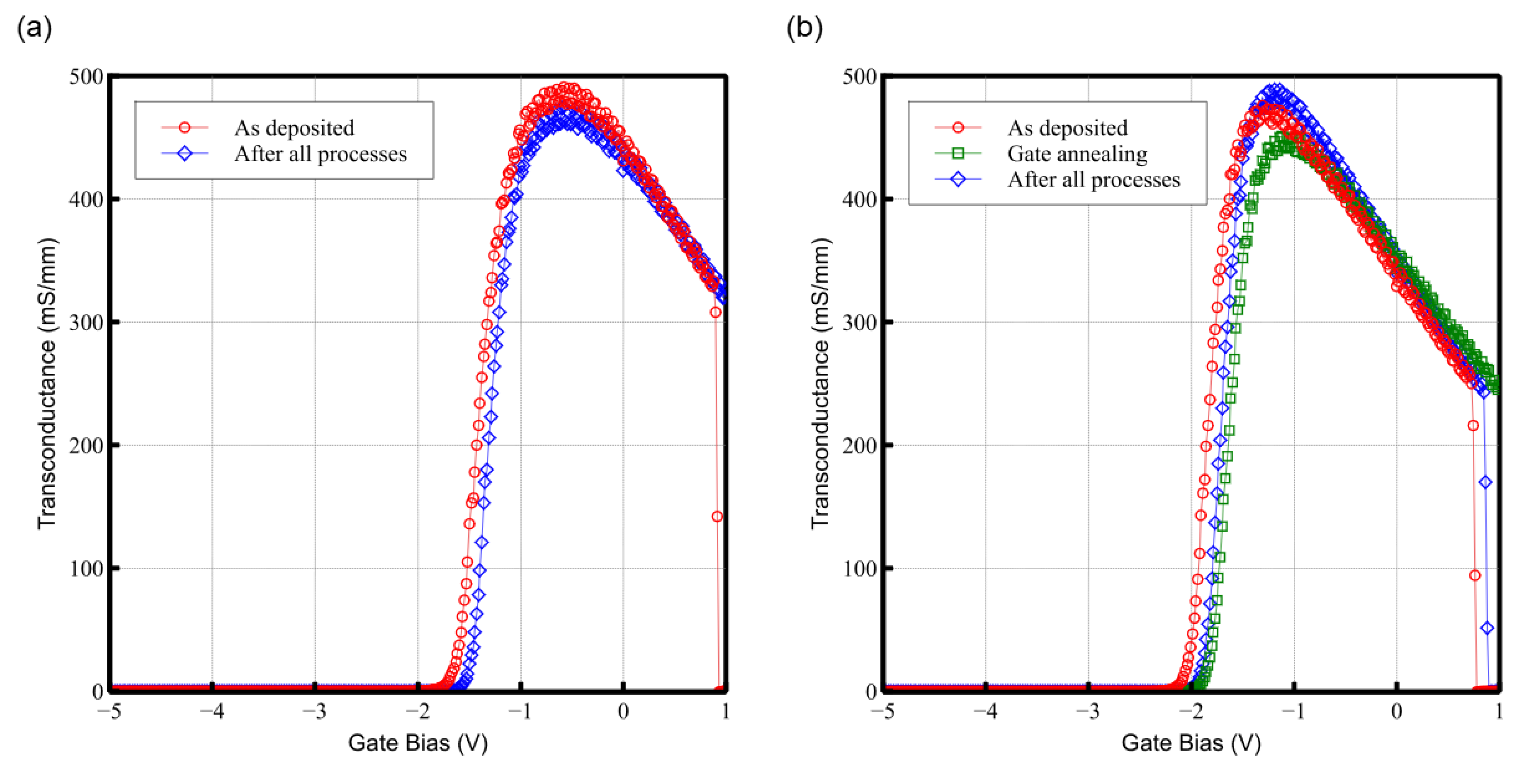
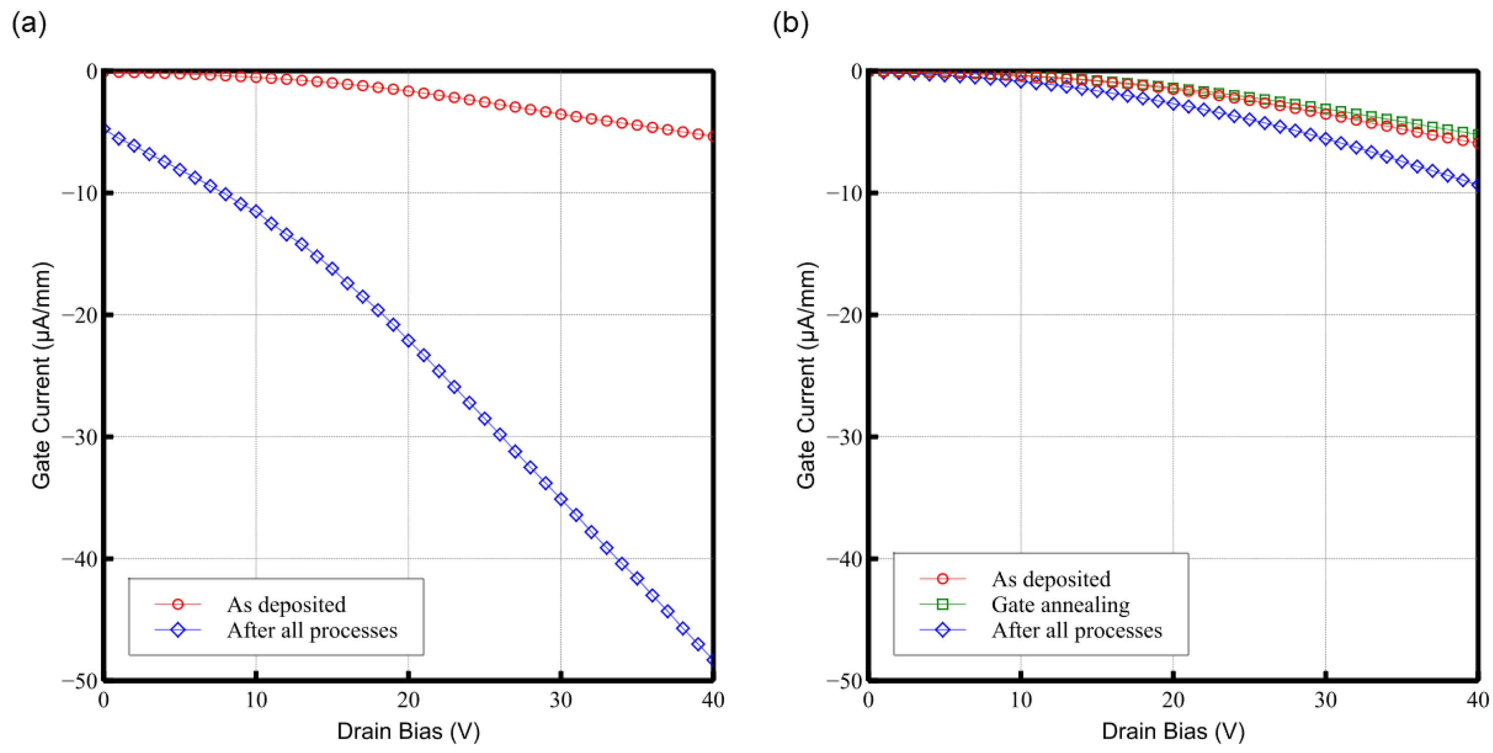
3.1. DC Characteristics

To analyze the electrical characteristics, DC measurements and RF measurements were performed. In the case of DC measurements, the devices with and without gate annealing were tracked according to the process progression. For each case, we measured immediately after gate metal deposition, after annealing for annealed devices, and after all processes by using Keysight HP4142. In each situation, we applied a drain voltage of 10 V and swept the gate voltage from −5 V to 1 V to obtain the Id-Vg curve and gm-Vg curve. Then, we applied a gate voltage of −5 V to turn off the channel and swept the drain voltage from 0 to 40 V to extract the gate leakage current and drain leakage current. Figure 2 is a graph of transconductance measured by applying a drain voltage of 10 V and varying the gate voltage from −5 V to 1 V.
Gate annealing was performed on one device and not on another. In the case of the device where gate annealing had not been performed, the maximum transconductance was measured as 491 mS/mm after the gate metal was deposited, and 475 mS/mm after all processes were completed. A slight decrease in maximum transconductance was observed. On the other hand, in the case of the device where gate annealing had been performed, the maximum transconductance was measured as 476 mS/mm after the gate metal was deposited, 451 mS/mm after gate annealing process, and 489 mS/mm after all processes. The maximum transconductance decreased after gate annealing, but increased after the process was completed compared to the initial value. This suggests that it exhibits a different behavior compared to devices that were not annealed.
The threshold voltage (Vth) was measured by the constant current method, with a criterion of 1mA/mm. For the device without gate annealing, the threshold voltage was measured as −1.48 V after gate metal deposition and −1.36 V after the completion of all processes. For the device with gate annealing, the threshold voltage was measured as −1.91 V after gate metal deposition, −1.69 V after annealing, and −1.75 V after the completion of all processes. Although there was an initial difference in the threshold voltage between the two devices after gate metal deposition due to process variations, the threshold shift was 0.12 V for the former and 0.16 V for the latter during the process.
Figure 3 shows the drain current change according to the gate bias voltage. Even when directly comparing the drain current, the difference is significant. In particular, for devices that did not undergo gate annealing, the off-state current at the end of the process was about 10 times higher than after gate metal deposition. However, for devices that underwent gate annealing, there was no significant difference. When the off-bias current is defined as Vgt = Vgs − Vth = −1 V, the off-bias current for the device without gate annealing was measured at 2.31 μA/mm after gate metal deposition and 31.9 μA/mm after the completion of all processes. For the device with gate annealing, the off-bias current was measured at 1.44 μA/mm after gate metal deposition, 1.44 μA/mm after annealing, and 3.19 μA/mm after the completion of all processes.
Figure 4 shows the gate leakage current change according to the drain bias for each case. In terms of leakage currents, a gate voltage of −5 V was applied, and the drain voltage was increased from 0 V to 40 V. For the wafer without annealing, when a drain voltage of 40 V and a gate voltage of −5 V were applied, the gate leakage current was measured at −5.36 μA/mm after gate metal deposition, and at −48.3 μA/m after the completion of the front-end process. For the wafer with annealing, the gate leakage current was measured at −5.93 μA/mm after gate metal deposition, −5.20 μA/mm after annealing, and −9.34 μA/mm after the completion of the front-end process.
The DC characteristics of AlGaN/GaN HEMTs with and without gate annealing were evaluated and compared in Table 1 through transconductance, threshold voltage (Vth), and leakage current measurements. The transconductance (gm) results revealed that for the device without gate annealing, there was a slight decrease in gm after the full process (from 491 to 475 mS/mm). However, the device with gate annealing showed a more dynamic behavior, where gm decreased after annealing but ultimately increased beyond the initial value after all processes were completed (from 476 to 489 mS/mm). This suggests that gate annealing may influence charge trapping at the gate interface, potentially improving the charge trapping dynamics and interface quality after the final process steps [26,27,28].
Gate leakage current showed significant differences. The device without gate annealing exhibited a dramatic increase in leakage current after the process (from −5.36 μA/mm to −4.83 μA/mm), likely due to increased charge trapping at the interface. In contrast, the annealed device maintained relatively stable leakage currents, with a moderate increase (from −5.93 μA/mm to −9.34 μA/mm), suggesting that gate annealing helps suppress the effects of charge trapping, reducing defects and improving the gate interface.

3.2. RF Characteristics

Afterward, the S-parameters within the frequency range of 0.5 to 50 GHz were evaluated using a Keysight N5245A microwave network analyzer, with gate voltage (Vg) set to 0 V and drain voltage (Vd) set to 0.8 V for the same device. The RF performance, including current gain (h21) and maximum stable/available gain (MSG/MAG), is shown in Figure 5. Using the above parameters, the cut-off frequency (ft) and the maximum frequency (fmax) were extracted. Similar to the DC measurements, both the device with gate annealing and the device without gate annealing were measured separately. Measurements were taken after all front-end processes were completed, and the results showed that the device without gate annealing had an ft of 48.87 GHz and fmax of 103.8 GHz, while the device with gate annealing had an ft of 52.98 GHz and fmax of 106.4 GHz. The improvements in RF efficiency were also notable. The RF efficiency increased by approximately 8.4%, as indicated by the enhanced power gain and reduced signal loss in high-frequency measurements. This improvement can be attributed to the better quality of the gate interface and reduced defect densities, which enhance carrier mobility and reduce scattering. The improved RF efficiency suggests that annealing can play a crucial role in optimizing HEMT performance for communication systems and other RF applications [17,22].
These results provide strong evidence for the beneficial effects of gate annealing on the performance of AlGaN/GaN HEMTs. Through a systematic measurement and analysis of the electrical characteristics before and after annealing, we have shown substantial improvements in key performance metrics. The process significantly decreases gate leakage currents, as demonstrated by the lower leakage in annealed devices compared to those without annealing. Furthermore, the improvements in RF performance, such as increased cut-off frequency (ft) and maximum frequency (fmax), emphasize the role of annealing in optimizing device efficiency for high-frequency applications.

4. Conclusions

The observed improvements in the Id-Vg and gm-Vg curves can be attributed to the annealing process reducing interface trap densities at the gate interface and within the GaN layer. The increase in peak transconductance and shift in threshold voltage indicate a more efficient channel formation and reduced scattering of charge carriers. This suggests that annealing helps in passivating surface states and repairing lattice damage caused during fabrication. The resulting improvement in carrier transport leads to better device performance, as reflected in the enhanced Id-Vg and gm-Vg characteristics. The significant reduction in gate and drain leakage currents post-annealing further supports this hypothesis. By decreasing the density of trap states and defects, the annealing process effectively minimizes leakage paths, enhancing the overall electrical integrity of the HEMTs. These findings underscore the importance of optimized annealing in the fabrication process, offering a pathway to achieving higher performance in RF applications. The reduced leakage currents contribute to lower power consumption and improved thermal management, which are critical for high-power devices.
While this study provides significant insights into the impact of gate annealing on GaN HEMTs, there are further characterization techniques that could deepen the understanding of the underlying mechanisms and enhance the overall analysis. For instance, multi-frequency C–V measurements could be employed to quantitatively assess the interface trap densities in devices with and without gate annealing, providing a more detailed evaluation of the gate interface’s quality. Additionally, load-pull measurements could be conducted to investigate the large-signal behaviors of GaN HEMTs, offering a more comprehensive analysis of the devices’ RF performance under high-power conditions. Also, stress testing under high-temperature and high-voltage conditions could be performed to assess the long-term reliability of the gate-annealed devices. These techniques present opportunities for future work and could provide further validation of the beneficial effects of gate annealing on device reliability and efficiency.

Author Contributions

Conceptualization, J.K.; methodology, J.K.; validation, J.K. and G.L.; Formal Analysis, J.Y.P., B.-G.M. and K.C.; Investigation, J.K., J.J. and H.-G.J.; Data Curation, J.K., J.J., W.C. and J.-M.L., writing—original draft preparation, J.K.; supervision, B.-G.M. and D.-M.K.; project administration, D.-M.K. All authors have read and agreed to the published version of the manuscript.

Funding

This research was financially supported by the Institute of Civil Military Technology Cooperation funded by the Defense Acquisition Program Administration and Ministry of Trade, Industry and Energy of Korean government under grant No. 22-CM-TN-15.

Data Availability Statement

The data presented in this study are available on request from the corresponding author.

Conflicts of Interest

The authors declare no conflicts of interest.

References

  1. Aadit, M.N.A.; Kirtania, S.G.; Afrin, F.; Alam, M.K.; Khosru, Q.D.M. High Electron Mobility Transistors: Performance Analysis, Research Trend, and Applications. In Different Types of Field-Effect Transistors-Theory and Applications; Intech: London, UK, 2017; pp. 45–64. [Google Scholar]
  2. Greco, G.; Iucolano, F.; Roccaforte, F. Review of Technology for Normally-Off HEMTs with p-GaN Gate. Mater. Sci. Semicond. Process. 2018, 78, 96–106. [Google Scholar] [CrossRef]
  3. Kumar, J.S.R.; Du John, H.V.; I.V, B.K.J.; Ajayan, J.; A, A.D.; Nirmal, D. A Comprehensive Review of AlGaN/GaN High Electron Mobility Transistors: Architectures and Field Plate Techniques for High Power/High Frequency Applications. Microelectron. J. 2023, 140, 105951. [Google Scholar] [CrossRef]
  4. Lee, J.M.; Min, B.G.; Chang, W.J.; Ji, H.G.; Cho, K.J.; Kang, D.M. Technical Trends in GaN RF Electronic Device and Integrated Circuits for 5G Mobile Telecommunication. Electron. Telecommun. Trends 2021, 36, 53–64. [Google Scholar]
  5. Mishra, U.K.; Parikh, P.; Wu, Y.F. AlGaN/GaN HEMTs—An Overview of Device Operation and Applications. Proc. IEEE 2002, 90, 1022–1031. [Google Scholar] [CrossRef]
  6. Kim, K.; Kim, T.J.; Zhang, H.; Liu, D.; Jung, Y.H.; Gong, J.; Ma, Z. AlGaN/GaN Schottky-Gate HEMTs with UV/O₃-Treated Gate Interface. IEEE Electron Device Lett. 2020, 41, 1488–1491. [Google Scholar] [CrossRef]
  7. Spelta, T.; Veillerot, M.; Martinez, E.; Mariolle, D.; Templier, R.; Chevalier, N.; Rocha, P.F.P.P.; Salem, B.; Vauche, L.; Hyot, B. Impact of Etching Process on Al2O3/GaN Interface for MOSc-HEMT Devices Combining ToF-SIMS, HAXPES, and AFM. Solid-State Electron. 2023, 208, 108743. [Google Scholar] [CrossRef]
  8. Yu, C.H.; Chiang, W.H.; Chen, Y.-H.; Samukawa, S.; Wuu, D.S.; Chung, C.-H.; Hsiao, C.-L.; Horng, R.H. Reduction of Interface Defects in Gate-Recessed GaN HEMTs by Neutral Beam Etching. Mater. Today Adv. 2024, 23, 100519. [Google Scholar] [CrossRef]
  9. Asubar, J.T.; Yatabe, Z.; Gregusova, D.; Hashizume, T. Controlling Surface/Interface States in GaN-Based Transistors: Surface Model, Insulated Gate, and Surface Passivation. J. Appl. Phys. 2021, 129, 123102. [Google Scholar] [CrossRef]
  10. Saito, W.; Kuraguchi, M.; Takada, Y.; Tsuda, K.; Omura, I.; Ogura, T. Influence of Surface Defect Charge at AlGaN-GaN-HEMT upon Schottky Gate Leakage Current and Breakdown Voltage. IEEE Trans. Electron Devices 2005, 52, 159–164. [Google Scholar] [CrossRef]
  11. Ahn, H.-K.; Kim, H.C.; Kang, D.M.; Kim, S.I.; Lee, J.M.; Lee, S.H.; Min, B.-G.; Yoon, H.-S.; Kim, D.-Y.; Lim, J.-W.; et al. Effect of Fluoride-Based Plasma Treatment on the Performance of AlGaN/GaN MISHFET. ETRI J. 2016, 38, 675–684. [Google Scholar]
  12. Kim, H.; Lee, J.; Liu, D.; Lu, W. Gate Current Leakage and Breakdown Mechanism in Unpassivated AlGaN/GaN High Electron Mobility Transistors by Post-Gate Annealing. Appl. Phys. Lett. 2005, 86, 142103. [Google Scholar] [CrossRef]
  13. Kumar, A.; Mukherjee, J.; Rawal, D.S.; Asokan, K.; Kanjilal, D. Trap Analysis on Pt-AlGaN/GaN Schottky Barrier Diode Through Deep Level Transient Spectroscopy. J. Semicond. 2023, 44, 042802. [Google Scholar] [CrossRef]
  14. Malik, A.; Sharma, C.; Laishram, R.; Bag, R.K.; Rawal, D.S.; Vinayak, S.; Sharma, R.K. Role of AlGaN/GaN Interface Traps on Negative Threshold Voltage Shift in AlGaN/GaN HEMT. Solid-State Electron. 2018, 142, 8–13. [Google Scholar] [CrossRef]
  15. Lee, H.-P.; Bayram, C. Improving Current ON/OFF Ratio and Subthreshold Swing of Schottky-Gate AlGaN/GaN HEMTs by Postmetallization Annealing. IEEE Trans. Electron Devices 2020, 67, 2760–2764. [Google Scholar] [CrossRef]
  16. Kim, H.; Schuette, M.L.; Lee, J.; Lu, W.; Mabon, J.C. Passivation of Surface and Interface States in AlGaN/GaN HEMT Structures by Annealing. J. Electron. Mater. 2007, 36, 1149–1155. [Google Scholar] [CrossRef]
  17. Lee, J.; Liu, D.; Kim, H.; Lu, W. Post-Annealing Effects on Device Performance of AlGaN/GaN HFETs. Solid-State Electron. 2004, 48, 1855–1859. [Google Scholar] [CrossRef]
  18. Chen, C.; Wang, Q.; Li, W.; Wang, Q.; Feng, C.; Jiang, L.; Xiao, H.; Wang, X. Effect of the Post-Gate Annealing on the Gate Reliability of AlGaN/GaN HEMTs. J. Semicond. 2021, 42, 092802. [Google Scholar] [CrossRef]
  19. Chung, J.W.; Roberts, J.C.; Piner, E.L.; Palacios, T. Effect of Gate Leakage in the Subthreshold Characteristics of AlGaN/GaN HEMTs. IEEE Electron Device Lett. 2008, 29, 1196–1198. [Google Scholar] [CrossRef]
  20. Stockman, A.; Canato, E.; Tajalli, A.; Meneghini, M.; Meneghesso, G.; Zanoni, E.; Moens, P.; Bakeroot, B. On the Origin of the Leakage Current in p-Gate AlGaN/GaN HEMTs. In Proceedings of the 2018 IEEE International Reliability Physics Symposium (IRPS), Burlingame, CA, USA, 11–15 March 2018; IEEE: Piscatvey, NJ, USA, 2018. [Google Scholar]
  21. Zhang, S.; Liu, X.; Wei, K.; Huang, S.; Chen, X.; Zhang, Y.; Zheng, Y.; Liu, G.; Yuan, T.; Wang, X.; et al. Suppression of Gate Leakage Current in Ka-Band AlGaN/GaN HEMT with 5-nm SiN Gate Dielectric Grown by Plasma-Enhanced ALD. IEEE Trans. Electron Devices 2020, 68, 49–52. [Google Scholar] [CrossRef]
  22. Jeong, J.; Cho, K.; Ji, H.; Chang, W.; Lee, J.; Min, B.G.; Kang, D. X-Band Quasi Class-F HPA MMIC Using DynaFET GaN HEMT Modelling. Electron. Lett. 2024, 60, e13221. [Google Scholar] [CrossRef]
  23. Efthymiou, L.; Longobardi, G.; Camuso, G.; Chien, T.; Chen, M.; Udrea, F. On the Physical Operation and Optimization of the p-GaN Gate in Normally-Off GaN HEMT Devices. Appl. Phys. Lett. 2017, 110, 123. [Google Scholar] [CrossRef]
  24. Chang, S.-J.; Jeong, H.S.; Jung, H.W.; Choi, S.M.; Choi, I.G.; Noh, Y.S.; Kim, S.-I.; Lee, S.-H.; Ahn, H.-K.; Kang, D.M.; et al. Effects of Parasitic Gate Capacitance and Gate Resistance on Radiofrequency Performance in LG = 0.15 μm GaN High-Electron-Mobility Transistors for X-Band Applications. ETRI J. 2024, 1–13. [Google Scholar] [CrossRef]
  25. Grünenpütt, J.; Sommer, D.; Splettstößer, J.; Chen OK, J.T.; Stieglauer, H.; Blanck, H. Evaluation of Novel Iron-Free QuanFINE® Structure by 100 nm and 150 nm AlGaN/GaN HEMT Technology. In Proceedings of the International Conference on Compound Semiconductor Manufacturing Technology (CS Mantech), Virtual, 24–27 May 2021. [Google Scholar]
  26. Wang, P.F.; Li, X.; Zhang, E.X.; Jiang, R.; McCurdy, M.W.; Poling, B.S.; Heller, E.R.; Schrimpf, R.D.; Fleetwood, D.M. Worst-Case Bias for High Voltage, Elevated-Temperature Stress of AlGaN/GaN HEMTs. IEEE Trans. Device Mater. Reliab. 2020, 20, 420–428. [Google Scholar] [CrossRef]
  27. Li, X.; Wang, P.; Qiu, H.; Zhang, E.; McCurdy, M.W.; Schrimpf, R.D.; Fleetwood, D.M. Irradiation-and Bias-Stress-Induced Charge Trapping and Gate Leakage in AlGaN/GaN HEMTs. In Proceedings of the 2022 22nd European Conference on Radiation and Its Effects on Components and Systems (RADECS), Venice, Italy, 3–7 October 2022; IEEE: Piscatvey, NJ, USA, 2022. [Google Scholar]
  28. Zhu, J.; Ma, X.; Hou, B.; Ma, M.; Zhu, Q.; Chen, L.; Yang, L.; Zhang, P.; Zhou, X.; Hao, Y. Comparative Study on Charge Trapping Induced Vth Shift for GaN-Based MOS-HEMTs with and without Thermal Annealing Treatment. IEEE Trans. Electron Devices 2018, 65, 5343–5349. [Google Scholar] [CrossRef]
Figure 1. (a) Structure of GaN HEMTs, (b) cross-sectional scanning transmission electron microscopy (STEM) image of GaN HEMTs, and (c) process flow chart.
Electronics 13 04038 g001
Figure 2. Graph of transconductance vs. gate bias voltage as process progresses, (a) without gate annealing process and (b) with gate annealing process.
Electronics 13 04038 g002
Figure 3. Graph of drain current vs. Vgt as process progresses, (a) without gate annealing process and (b) with gate annealing process. X-axis is Vgt = Vgs − Vth.
Electronics 13 04038 g003
Figure 4. Graph of gate leakage current vs. drain bias voltage as the process progresses, (a) without gate annealing process and (b) with gate annealing process.
Electronics 13 04038 g004
Figure 5. Graph of the RF performance, including current gain (h21) and maximum stable/available gain (MSG/MAG), (a) without gate annealing process and (b) with gate annealing process.
Electronics 13 04038 g005
Table 1. Transconductance, gate leakage current, and threshold voltage (Vth) according to the wafer and process. Wafer 1 indicates the device which did not undergo the gate annealing process, while wafer 2 did undergo the process. Transconductance was measured by applying a drain voltage of 10 V, and gate leakage current was measured by applying a drain voltage of 40 V and gate voltage of −5 V.
DeviceStatusgm (mS/mm)Ig.leak (μA/mm)Vth (V)Id.off (μA/mm)
Wafer 1As deposited491−5.36−1.480.231
Wafer 1After all processes475−48.3−1.363.19
Wafer 2As deposited476−5.93−1.910.144
Wafer 2Gate annealing451−5.20−1.690.144
Wafer 2After all processes489−9.34−1.750.319
Disclaimer/Publisher’s Note: The statements, opinions and data contained in all publications are solely those of the individual author(s) and contributor(s) and not of MDPI and/or the editor(s). MDPI and/or the editor(s) disclaim responsibility for any injury to people or property resulting from any ideas, methods, instructions or products referred to in the content.

