Abstract
In high-power applications, achieving adequate power quality in power converter design is accomplished by utilizing multilevel inverters instead of using two-level and three-level inverters. The device generates a sinusoidal output voltage, which results in reduced total harmonic distortion and lower voltage stress on the switches and leads to lower electromagnetic interference, making it suitable for use in renewable energy applications. However, to illustrate the advantages mentioned above, a significant number of switching devices and DC sources are necessary while raising the voltage levels. This article proposes an asymmetrical voltage generation method, which operates in a ratio of 1:5 and generates 25 levels using 11 power switches. The topology is modular in structure, and each module has a lower component count, which significantly reduces the overall cost. The proposed topology is capable of generating negative output voltage levels without the use of an H-bridge configuration, where only three switches are used to generate any voltage levels. The functionality of the developed module is amended by fixing different voltage values in DC sources. This article also presents a comprehensive examination of the circuit and the functioning of various voltage levels. The advantages of the proposed inverter have been demonstrated by comparative research with the currently existing MLI topologies. Ultimately, both the simulation and experimental findings validated the practical capabilities.
1. Introduction
Multilevel inverters (MLIs) have become increasingly significant in renewable energy systems due to their capacity to generate high-quality power output with minimal harmonic distortion. MLIs effectively transform direct current (DC) from renewable sources into alternating current (AC), thereby increasing compatibility with the power grid and improving overall system efficiency [1,2]. The automotive industry, which plays a crucial role in global economic dynamics, is undergoing a rapid evolution with the emergence of electric vehicles (EVs) and autonomous driving technologies taking the lead [3,4]. Aircraft applications encompass both commercial and military aviation, including passenger transport, cargo delivery, and combat missions. Innovations include advanced materials for lighter, stronger structures, cutting-edge propulsion systems, and autonomous flight technologies to enhance safety and efficiency [5]. Reactive power compensation makes the power system more efficient by integrating the supply and demand of reactive power, which lowers losses and makes the voltage more stable [6,7,8]. It claims its advantages in terms of generating a stepped voltage closer to a sinusoidal shape through several isolated DC sources, dc-link capacitors, clamping diodes, or capacitors. Several researchers have developed MLIs with novel topologies, carrier-based modulation strategies, and closed-loop control [9]. Many topologies have originated from traditional cascaded H-bridge MLIs to reduce total components and modulation strategies from phase/level-shifted carrier PWM methods. Over the past few years, there have been notable improvements in the field of electrical engineering, specifically in the areas of circuit design and power electronics [10]. One of the key innovations that has revolutionized the way electrical systems are constructed and operated is the H-bridge configuration [11]. The H-bridge, a fundamental component in power electronics, enables efficient control of voltage polarity and magnitude, making it indispensable in a wide range of applications including motor control, power conversion, and renewable energy systems [12,13]. Moreover, the comparative analysis of circuits with and without H-bridge configurations is incorporated as well. The H-bridge structure is used in circuits that are specifically designed for renewable energy applications. This design incorporates a revolutionary multisource switching capacitor architecture, as described in references [14,15,16]. By using low-power semiconductor switches and capacitors, this system utilizes a binary charging/discharging algorithm with series/parallel modes. As a result, it eliminates the requirement for circuit balance. Notably, it integrates a dual-input nine-level inverter featuring trinary voltage ratios to minimize active switches, augmenting reactive power capability through the integration of bidirectional switches. In addition, it demonstrates a switched capacitor module that produces voltage sources with 9 levels and 21 levels. This eliminates the need for H-bridge operation and reduces the use of high-blocking voltage switches. Furthermore, a tapped source stack (TSS) and a modified H-bridge inverter are proposed to function in a single stage, buttressed by multicarrier pulse width modulation implementation. This innovative MLI optimizes switch count for targeted voltage levels, pledging a higher voltage output with fewer components and bolstered performance, while concomitantly curtailing overall power device requisites, size, cost, and intricacy [17,18]. In contrast, several different MLI topologies are presented for renewable energy applications. For example, a cascaded structure with three DC sources and bidirectional switches requires an H-bridge inverter for polarity reversal, indicating potential in photovoltaic (PV) applications. Another topology, employing four DC sources with bidirectional and unidirectional switches, achieves high-quality output voltage yet demands a surplus of switching devices. Moreover, a structure employing five DC sources and twelve switches yields stepped voltage, accentuating the utilization of bidirectional switches with high blocking voltage. An innovative modified matrix structure MLI heightens output levels via a flexible configuration, thereby diminishing the number of switching devices [19,20,21,22,23]. These advancements portend efficient utilization of renewable energy with enhanced voltage control and diminished component complexity.
This research paper deals with a new topology with asymmetric DC sources, and the novelty of the MLI can be summarized as follows:
- (a)
- It employs eleven switches and four DC sources to generate a waveform with 25 levels of output voltage.
- (b)
- The proposed MLI does not require an H-bridge for negative polarity generation.
- (c)
- The proposed topology was initially modeled and simulated using the MATLAB/Simulink 2019b platform.
- (d)
- A 25-level inverter is proposed, simulated, and designed in the laboratory. The experimental results validate the smooth operation of the inverter.
- (e)
- Only three switches are conducted to generate any voltage levels.
- (f)
- The staircase waveform enhances power quality and lowers overall total harmonic distortion (THD).
This article is organized into distinct sections. Section 2 methodically summarizes the developed topology. Section 3 offers a comprehensive review of existing topologies, setting the stage for comparative analysis. Following this, Section 4 presents the empirical results obtained through simulation and experimentation. Finally, Section 5 encapsulates the conclusions drawn from the study, highlighting the significance of the findings and avenues for future research.
2. Proposed Modular Structure Topology
In this structure, four DC sources and eleven power switches are employed to generate 25 voltage levels across the output. Figure 1 depicts the circuit configuration, where a DC voltage ratio of 1:5 is employed to generate 25 voltage level outputs. The proposed topology is designed to function with various magnitudes of source voltage in order to achieve high voltage levels. Switches T1–T6 are only unidirectional, while switches T7–T11 are bidirectional. The proposed topology can be easily extended in a modular structure to generate n levels of output voltage, as depicted in Figure 2.

Figure 1.
Proposed 25−level inverter configuration.
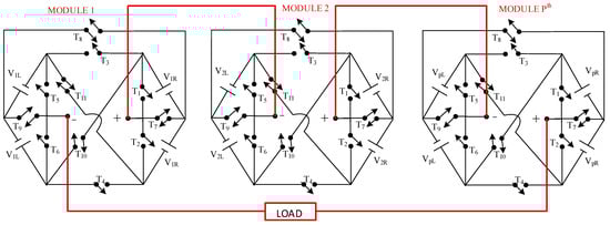
Figure 2.
Generalized modular structure of proposed MLI.
The bidirectional switches are derived from the common emitter configuration of two unidirectional IGBTs, utilizing a single gate driver circuit to provide cost-effective real-time implementation [7]. Table 1 illustrates the operating mode of the proposed topology. A tick mark (✔) in the table indicates that the corresponding switch is ON for the particular positive voltage level shown in the second column of the table. A cross mark (✘) signifies that the corresponding switch is switched ON for the negative voltage level represented in the 14th column of the table. The switches T1, T4, and T6 are ON to achieve +2 Vdc, as depicted in Mode 2 of Figure 3, whereas the switches T2, T3, and T5 are switched ON to achieve −2 Vdc, as depicted in Mode 15 in Table 1. Similarly, the switches T2, T9, and T10 are switched ON to generate +3 Vdc, whereas the switches T1, T9, and T11 are switched ON to generate −3 Vdc, as depicted in Mode 16 in Table 1. It should be said that only three switches out of eleven switches are operated at a time to generate a particular voltage level.

Table 1.
Different switching states for 25−level inverter: positive level (✔), negative level (✖).
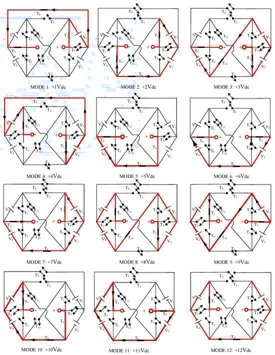
Figure 3.
Switching states for 25−level inverter (12 positive voltage levels).
The proposed structure has the capability of cascading to acquire higher voltage levels. For example, two proposed modules are cascaded to produce 49 levels of voltage in the output voltage. The switching sequence to obtain various voltage levels can be observed in Figure 3 and Table 1.
The other important parameter in design aspects is the total blocking voltage of the switches used in the developed topology. The blocking voltage of the switches T1, T2, and T7 is decided by the voltage sources V1R = V1 = 1 Vdc and V1R = V2 = 1 Vdc, and the switches T5, T6, and T9 are calculated by the voltage sources V1L = V3 = 5 Vdc and V1L = V4 = 5 Vdc, while the switches T10, T11, T3, and T4 are determined by the voltage sources V1R = V1 = 1 Vdc, V1R = V2 = 1 Vdc, V1L = V3 = 5 Vdc, and V1L = V4 = 5 Vdc. In addition, the blocking voltage of the switch T8 is calculated by the voltage sources V1R = V1 = 1 Vdc and V1L = V3 = 5 Vdc. Therefore, the total standing voltage (TSV) of the switches is 84 Vdc and is determined as depicted in Table 2.
Table 2.
Blocking voltage distribution of the proposed topology for Module 1 (p = 1).
The blocking voltage of the switches is determined by the magnitude of the DC voltage source, whereas the total standing voltage, determined by the summation of the magnitude of DC voltage sources, are used in the proposed topology. The proposed structure does not require an H-bridge to generate negative voltage levels; therefore, the proposed topology would experience less TSV than the configuration using an H-bridge inverter. Thus, it can be concluded that the configuration generates more voltage levels with a variety of DC sources.
2.1. Cascaded Operations
By connecting multiple modules together, the voltage levels can be expanded as needed. The basic structure of the proposed topology produces 25 voltage levels. Using a variety of cascaded modules, Figure 2 depicts the generalized structure of the proposed topology. Each module is cascaded together to enhance the voltage levels and to demonstrate the direct link between the module number and harmonic distribution. The voltage level is generated based on the voltage ratio of input DC sources. The two different voltage ratios for the proposed inverter are elaborated as two different cases, described below as Case 1 and Case 2, respectively.
2.1.1. Case 1 (For Identical Voltage Ratios in All Modules)
Table 3 illustrates the various properties of the cascaded structure for a group of ‘p’ modules. In Figure 3 shown above, DC voltage sources and their respective values are selected in the ratio of 1:5, and details about the module are given in Table 3. In the first module (p = 1), there are 25 levels generated with only sixteen IGBTs/diodes, eleven gate drivers, and four DC sources. Similarly, in the second module (p = 2), when cascaded with the first module, there are 49 levels generated with only 32 IGBTs/diodes, twenty-two gate drivers, and eight DC sources. Similarly, in the pth module (p = p), there are (24p + 1) levels generated with only 16p IGBTs/diodes, 11p gate drivers, and 4p DC source. Thus, it can be said that upon doubling the required components, voltage levels can be linearly increased with nearly a double count.
Table 3.
Relationship between various design parameters in terms of (p) for 1:5 voltage ratio.
2.1.2. Case 2 (For Voltage Ratio of 52t:52t+1, Where t = p−1 and ‘p’ is the Module)
Each module is cascaded together in order to generalize the provided topology with the voltage ratio of 52t:52t+1, where t = p-1 and ‘p’ is the number of modules cascaded. Table 4 illustrates the various properties of the cascaded structure for a group of ‘p’ modules. Details about the module are given in Table 4 below; as with the first module (p = 1), there are 25 levels generated with only sixteen IGBTs/diodes, eleven gate drivers, and four DC sources. Similarly, in the second module (p = 2), when cascaded with the first module, there are 625 levels generated with only 32 IGBTs/diodes, twenty-two gate drivers, and eight DC sources. Similarly, in the third module (p = 3), when cascaded with the first and second modules, there are 15,625 levels generated with only forty-eight IGBTs/diodes, thirty-three gate drivers, and twelve DC sources. Similarly, in the pth module (p = p), there are 25p levels generated with only 16p IGBTs/diodes, 11p gate drivers, and 4p DC sources. Thus, it can be observed that upon nearly doubling the required component count, the voltage levels increase abruptly, in a non-linear manner.
Table 4.
Relationship between various design parameters for DC voltage ratio of 52t:52t+1.
It can be clearly observed in Case 1, with the same voltage ratio of 1:5 in all the cascaded modules, that the voltage level of the consecutive module is almost double its previous one. Meanwhile, in Case 2, it can be observed that when the voltage ratio is 52t:52t+1, the voltage levels are increasing enormously.
A brief description of the output voltage of the proposed topology for Case 1 and Case 2 is shown in Table 5 and Table 6. Module 1 (m1) of both cases shows the same output voltage, while there is a remarkable difference in output voltage between Case 1 and Case 2 for Module 2 (m2): the output voltage of Case 2 is 25 times that of Case 1. For a better understanding, the parameters of the generalized cascaded MLI with ‘p’ modules of Case 1 and Case 2 are shown in Table 7.
Table 5.
Generated output voltage levels of the cascaded inverter modules with a voltage ratio of 1:5.
Table 6.
Generated output voltage levels of the cascaded inverter modules with a voltage ratio of 52t:52t+1.
Table 7.
Parameters of the generalized cascaded MLI with ‘p’ modules operating under Case 1 and Case 2.
However, with different DC link voltages, the cascaded combination of the aforementioned inverter modules can generate much higher voltage levels with the same number of components (Case 2), as depicted in Table 4. Module 1 can generate 49 voltage levels of magnitude with different DC link voltages (Case 1). The voltage levels has shown in Table 8. Module 2 can generate 625 voltage levels of magnitude, i.e., 25 times those of Module 1 (+300, +275, …, −275, −300). Thus, the output voltage levels of the 625-level inverter, which can be generated by cascading the same two inverter modules with different DC link voltages (Case 2) in Module 2 (25 times Module 1) ranging from −312 to +312 (312 positive voltage levels, 312 negative voltage levels, and a 0 voltage level), are depicted in Table 9.
Table 8.
Case 1 (49 voltage levels with identical DC voltage ratio in both modules).
Table 9.
Case 2 (625 voltage levels with different DC voltage ratios in both modules).
At a voltage ratio of 1:5, across the module, as depicted in Figure 4a, the blocking voltage is distributed within the module. Similarly, for the voltage ratio of 52t:52t+1, the distribution of blocking voltage is investigated as depicted in Figure 4b. It can be clearly concluded while selecting the topology for a voltage ratio of 1:5 that the blocking voltage remains the same in each module, whereas the blocking voltage of three modules for the other voltage ratio of 52t:52t+1 is dangerously high, leading to a higher overall cost for the component. The blocking voltages are studied across different modules, as depicted in Figure 4.
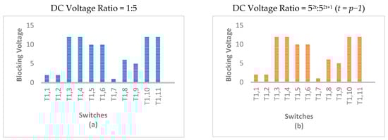
Figure 4.
Blocking voltage distribution for Module 1 with a voltage ratio of (a) 1:5, (b) 52t:52t+1 (t = p − 1).
3. Comparison Study
The circuit design section elucidates two configurations: one employing an H-bridge and another without an H-bridge. The circuits with an H-bridge have been depicted in Figure 5 and the circuits without H-bridge have been depicted in Figure 6. The H-bridge variant offers enhanced control and efficiency by facilitating bidirectional power flow and reduced losses. Contrarily, the non-H-bridge circuit, while simpler, lacks the flexibility and robustness of its counterpart.
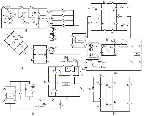
Figure 5.
Recently published inverter circuits with H-bridge configuration (a) [14]; (b) [15]; (c) [16]; (d) [17]; (e) [18]; (f) [19]; (g) [20]; (h) [21].
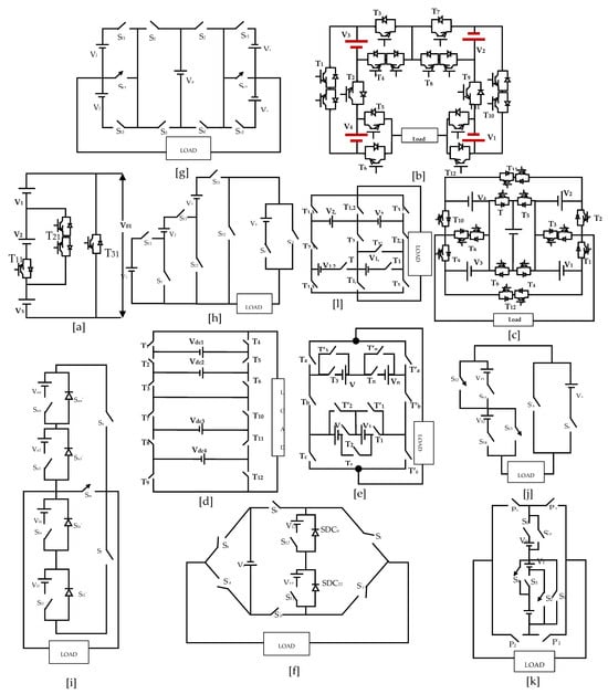
Figure 6.
Recently published inverter circuits without H-bridge configuration (a) [22]; (b) [23]; (c) [24]; (d) [25]; (e) [26]; (f) [27]; (g) [28]; (h) [29]; (i) [30]; (j) [31]; (k) [32]; (l) [33].
3.1. Comparison of Inverter Circuits with H-Bridge Configuration [14,15,16,17,18,19,20,21]
A multisource switched capacitor topology for renewable energy applications has been portrayed using reduced-power semiconductor switches and capacitors. The topology uses fewer capacitors which charge/discharge in a binary algorithm using series/parallel modes without the use of any circuit balancing [14]. A dual-input 9-level inverter with a trinary voltage ratio is presented to offer the minimum current-conducting switches. The topology is realized for reactive power capability by replacing unidirectional switches with bidirectional switches [15]. A novel switched capacitor module is developed to produce 9-level and 21-level inverters in similar and asymmetrical voltage sources. The topology eliminates H-bridges in its operation to reduce high-blocking-voltage switches, and a new switching scheme is used to self-balance the capacitor voltages [16]. The DC sources are arranged in a parallel/series combination through a set of switching devices to offer high-quality output voltage, and the topology requires a large number of bidirectional switching devices, which are used in limited applications [17].
A single-stage novel MLI is presented in [18], featuring a modified H-bridge inverter and a tapped source stack (TSS). The application of a field-programmable gate array (FPGA) for developing multicarrier pulse width modulation is also described.
The reduction in the overall power of devices such as power semiconductor switches, gate drivers with their associated circuits, and DC voltage sources reduces their size, cost, and complexity. A multicarrier pulse width modulation strategy is adopted to generate the switching pulses. The authors of [19,20] discussed the calculation of switching losses as well as the conduction losses. In this proposed H-type inverter, 17 voltage levels can be generated using nine power switches. Moreover, a 49-level inverter is developed based on the first algorithm of the proposed MLI; various performance parameters are compared to prove the effectiveness of the proposed MLI [21].
3.2. Comparison of Inverter Circuits without H-Bridge Configuration [22,23,24,25,26,27,28,29,30,31,32,33]
A cascaded three-DC-source structure using several bidirectional switches to produce a stepped voltage was created, and the topology requires an H-bridge inverter for polarity reversal. The topology was realized in PV applications to demonstrate its utility in renewable energy applications [22]. A four-DC-source MLI topology with several bidirectional and unidirectional switches to offer high-quality output voltage was created. The topology requires a large number of bidirectional switching devices and current-conducting devices [23]. A new structure based on five DC sources and twelve switches was used to produce a stepped voltage, and the cascaded structure was obtained by using several basic units. The structure uses several bidirectional switches with a high blocking voltage [24]. A cross-connected DC source with fewer switches to optimize voltage levels was developed to reduce total power components. However, the topology follows the traditional cross-connected voltage source’s structure, and the novelty is its asymmetrical operation with high blocking voltage [25]. The concept of the proposed modified matrix structure multilevel inverter (MMSMLI) involves arranging switches in columns and separate DC sources (SDCs) in row links. This arrangement facilitates easy addition and subtraction of SDCs, which is particularly beneficial for asymmetrical operation, enabling the creation of more output levels. Additionally, introducing cross-switching in the matrix structure helps reduce the number of switching devices in the current conduction path across various output voltage levels [26]. Another proposed design, the flexible rung ladder-structured multilevel inverter (FRLSMLI), essentially extends a ladder-structured bridge (H-bridge with additional rungs). These rungs consist of either source inclusion–bypass cells (SIBCs) or four-level creator cells (FLCCs). The FRLSMLI can synthesize fifteen levels using three SDCs, with simulation and experimental results validating its applicability in real-time applications [27]. A novel generalized modular MLI topology combines the unique advantages of existing MLIs to enhance output voltage levels while incorporating a comparatively lower number of power electronic components, maintaining similar performances [28].
Furthermore, the proposed configurations include a specimen 27-level inverter modulated using sinusoidal pulse width modulation (SPWM) and implemented in a laboratory prototype setup using a d-SPACE 1103 controller. Real-time experimental results are presented and verified against simulation results for both 7-level and 13-level inverters across RL-Load [29,30]. Two new structures of MLIs are introduced based on a modified T-type inverter and switched-diode cell. These inverter topologies are cascaded in series due to their generalized structure, with the inherent property of generating negative voltage levels without using any full H-bridge circuit being a key feature [31]. Additionally, a generalized cascaded multilevel inverter is proposed, employing only a half-bridge converter for polarity reversal, thus reducing the required number of power switches [32]. Lastly, a single-phase cascaded generalized doubling circuit-based MLI configuration is presented, capable of generating the maximum number of output voltage levels by distributing the total asymmetrical input DC link voltage among the cells using a minimum number of power switches [33].
A comparison of the proposed topology with other topologies (with and without H-bridges) based on total switches, DC sources, number of voltage levels, number of switches in the current conduction path, and gate drivers is depicted in Table 10.
Table 10.
Component counts with several recent MLI configurations.
The proposed multilevel inverter (MLI) topology in Table 10 is compared with various existing topologies in terms of component counts, such as total switches, gate drivers, DC sources, number of voltage levels, and switches in the current conduction path. The proposed topology requires 11 total switches and 11 gate drivers, which is relatively efficient compared to topologies with higher component counts like those in references [14,19] and [24]. The proposed topology requires fewer DC voltage sources compared to many existing topologies to achieve equivalent output levels. For instance, the topology referenced in [24] requires five DC sources to generate 27 levels of output, and the topology referenced in [29] also needs five DC sources to produce 27 levels. In contrast, the proposed topology only requires four DC sources to generate 25 levels of output, demonstrating greater efficiency in component utilization. Additionally, the proposed topology has only three switches in the current conduction path, indicating a lower conduction loss compared to most other topologies, making it a balanced choice in terms of efficiency and performance.
4. Simulation and Experimental Studies
This section portrays the simulation and experimental investigation of the developed topology in the MATLAB/Simulink platform and a laboratory prototype arrangement. The design of a low-power laboratory prototype of a single-phase reduced-switch MLI has been explained for experimental verification. The proposed single-phase 25-level inverter consists of six unidirectional and five bidirectional controlled switches. The unidirectional controlled switches are realized using an insulated gate bipolar junction transistor (IGBT) with an anti-parallel diode. The bidirectional controlled switches are realized using an IGBT with four ultra-fast diodes.
In practice, the selected rating of the devices (voltage and current) must be greater than the theoretical (calculated) values by 1.5 to 2.0 times for the safety of the switches. However, due to its availability in the laboratory, the IGBT CT60AM-18F is used in the design of the proposed inverter. The proposed 25-level inverter prototype model uses the following components: power switch—CT60AM IGBT, TLP250 (gate driver circuits), isolated DC sources, DSO-X 2024A (Key sight Technologies), and Resistive Inductive Load.
The prototype of the proposed inverters is developed using the DC sources obtained by the multiple isolated winding transformers, rectifiers, and arrangements of the capacitive filter, as shown in Figure 7a. The NLC gate pulse for the proposed MLI that is obtained from the DS1103 is fed to the converter/inverter switches through the DS1103 connector and the isolated gate drivers. Figure 7b shows the complete hardware setup of the proposed 25-level inverter-based system, which shows the power components (inverter, transformer, etc.) and the d-SPACE controller (DS1103) along with the measuring devices. The bidirectional IGBTs are obtained by using two unidirectional IGBTs in a common emitter configuration in simulation, and the same is used in the experimental setup. The blocking voltage in the MLI is the voltage rating that every switching device has to endure when it is in the OFF state. Overvoltage can cause semiconductor devices to fail and possibly damage the inverter circuit as a whole. Therefore, in order to ensure dependability and safe operation, choosing switching devices with the proper voltage ratings is essential in MLI design. The blocking voltage across switches S1, S2, S3, S4, S5, S6 S7, S8, S9 S10, and S11 is 50 V, 50 V, −300 V, 300 V, −250 V, −250 V, 25 V, 150 V, 125 V, 250 V, and −250 V, respectively, as depicted in Figure 8. The magnitudes of the maximum blocking voltage across the switches are S3 = 12 Vdc, S4 = 12 Vdc, S5 = 10 Vdc, and S6 = 10 Vdc and the minimum blocking voltages across the switches are S7 = Vdc, S1 = 2 Vdc, S3 = 2 Vdc, S9 = 5 Vdc. The selection of power switches is carried out accordingly to reduce the cost of the proposed MLI. To optimize the cost of the inverter, the blocking voltage is the most important aspect of the inverter.
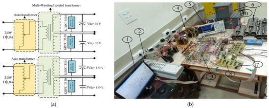
Figure 7.
(a) Schematic diagram of multi-winding isolated transformer, (b) Experimental setup in the laboratory for the proposed modular inverter. 1: host PC. 2: DS1103. 3: multimeter. 4: Multi-winding Isolated Transformer with rectifier and filter arrangements (realization of DC sources). 4: Multi-winding Isolated Transformer with rectifier and filter arrangements (realization of DC sources). 6: resistive road. 7: delay board or dead-band board. 8: DC supply to driver circuits. 9: proposed inverter. 10: inductive load.
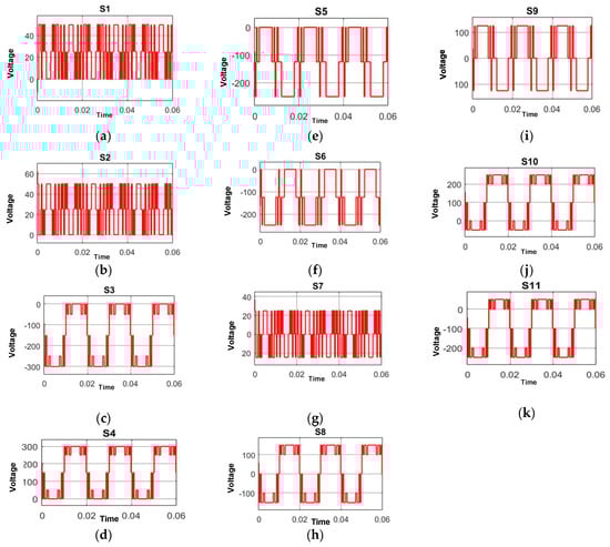
Figure 8.
Blocking voltages across the switches: (a) S1, (b) S2, (c) S3, (d) S4, (e) S5, (f) S6, (g) S7, (h) S8, (i) S9, (j) S10, (k) S11.
In the simulation, the input voltage values are V1 = V2 = 25 V and V3 = V4 = 125 V. Referring to Table 11, both simulation and experimentation are conducted with two distinct loads: one with R = 180 Ω, L = 25 mH, and the other with R = 180 Ω, L = 150 mH. The simulation and experimentation analysis are performed with a modulation index (MI) of 0.8 and 1 for the 25-level inverter. Figure 9 illustrates the outcomes of both simulation and experimentation for the load current and output voltage for R = 180 Ω and L = 25 mH at MI = 0.8. The measured Vo/p stands at 275 V, as depicted in Figure 9a, while the load current is recorded at 1.2 A, as depicted in Figure 9b. The experimental results for the output voltage and load current, as depicted in Figure 9c, match the values obtained from the simulation.
Table 11.
Circuit parameters in simulation and experimental tests for proposed 25-level inverter.
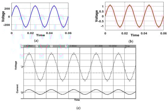
Figure 9.
Simulation results for the (a) output voltage and (b) load current. (c) Experimental results for the output voltage and the load current at modulation index 0.8 for L = 25 mH, R = 180 Ω.
The simulation results of output voltage and load current are depicted in Figure 10a and Figure 10b, respectively, for the load R = 180 Ω and L = 150 mH at MI = 0.8. Specifically, the load current is reported as 0.9 A, while the output voltage is measured at 259.2 V. Figure 10c presents the corresponding experimental results, which validate the simulation results, ensuring the accuracy and reliability of the simulation model.
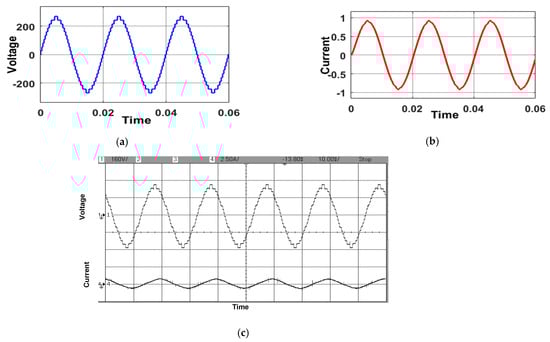
Figure 10.
Simulation results for the (a) output voltage and (b) load current. (c) Experimental results for the output voltage and load current at modulation index 0.8 for L = 150 mH, R = 180 Ω.
Figure 11 illustrates the comparative results between simulation and experimental data for the output voltage and load current under specific conditions: R = 180 Ω, L = 25 mH, at MI = 1. The load current registers at 1.3 A, while the measured value of the output voltage stands at 301 V. The simulation results of output voltage and load current are depicted in Figure 11a and Figure 11b, respectively, while Figure 11c illustrates the experimental results of load current and output voltage. It can be observed that the results obtained from the simulation and experimentation are nearly equal.
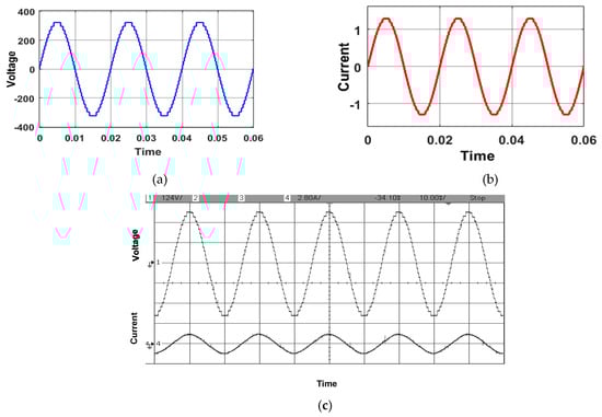
Figure 11.
Simulation results for the (a) output voltage and (b) load current. (c) Experimental results for the output voltage and the load current at modulation index 1 for L = 25 mH, R = 180 Ω.
In Figure 12, the outcomes of both simulation and experimental tests are depicted for the output voltage and load current under the conditions of R = 180 Ω, L = 150 mH, and MI = 1. The load current measures at 1.1 A, with the recorded value of Vo/p being 301 V. Figure 12a,b show the simulation outcomes for the output voltage and load current, respectively, whereas Figure 12c depicts the experimental data for both load current and output voltage, validating the simulation results.
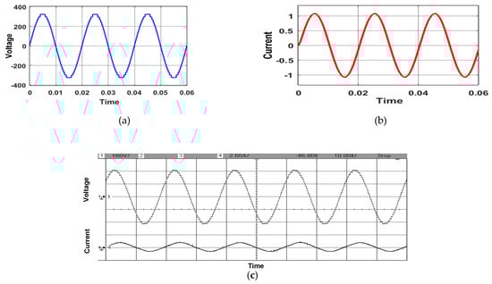
Figure 12.
Simulation results for the (a) output voltage and (b) load current. (c) Experimental results for the output voltage and load current at modulation index 1 for L = 150 mH.
Figure 13 depicts the experimental results for the output voltage and load current with variable modulation indexes ranging from 0.8 to 1 for two different loads. The experimentation is conducted with two distinct loads: one with R = 180 Ω, L = 25 mH, as depicted in Figure 13a, and the other with R = 180 Ω, L = 150 mH, as depicted in Figure 13b.
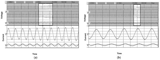
Figure 13.
Experimental result for the output voltage and load current with varying modulation index from 0.8 to 1 with (a) L = 25 mH and (b) L = 150 mH.
The total harmonic distortion (THD) values for MI of 1 and 0.8 are illustrated in Figure 14a and 14b, respectively. The THD value for MI = 1 is 3.28%, while for MI = 0.8, it is 4.58%. It can be observed that with a decrease in MI, the value of THD is increased, which is the reason why an MLI is preferred to be used at maximum MI.
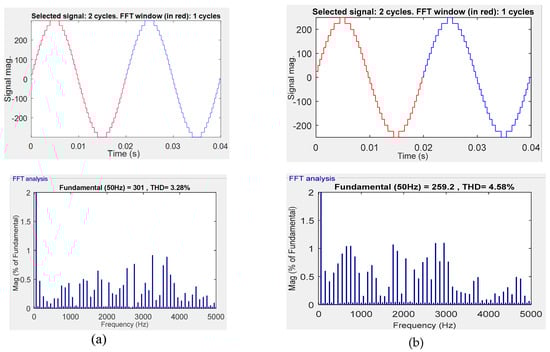
Figure 14.
Total harmonic distortion of output voltage of proposed 25-level inverter for (a) MI = 1; (b) MI = 0.8.
The power rating of the inverter is 1000 VA. In order to show the performance of the proposed MLI, the inverter is simulated in MATLAB/Simulink using PLECS Blocksets for R-load (R = 62 Ω). The inverter parameters for a specimen output power of 1016 W are considered, with a peak inverter output voltage of 360 V, a fundamental frequency of f = 50 Hz, and an input DC-link voltage of Vdc = 30 V and 5 Vdc = 150 V. The total power input to the inverter is 1026 W. The sum of all conduction losses across the switches is 9.2787 W. The total switching loss for all switches is 0.2588 W. The total loss (sum of conduction and switching losses) in the MLI is 9.5375 W. The output power is calculated by subtracting the total loss from the input power, which is 1016.463 W. So, the efficiency of the MLI is 99.07%, indicating that only a small fraction of power is lost during the operation. Conduction loss is the predominant form of loss compared to switching loss.
The highest switching loss occurs in switch S7, as it is heavily involved in generating the 25-level output, turning on and OFF ten times per cycle. In contrast, switch S8 experiences the lowest switching loss due to its minimal involvement in producing the 25-level output, switching ON and OFF only four times per cycle. Figure 15a–c show the bar graphs for the switching loss, conduction loss, and total loss of the eleven individual switches, respectively.
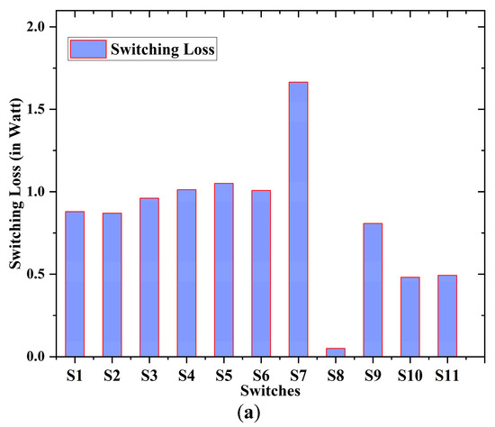

Figure 15.
Loss distribution of individual power switches: (a) switching loss, (b) conduction loss, (c) total loss.
Conduction losses occur when current flows through the semiconductor switches (such as MOSFETs, IGBTs, or other devices). These losses depend on the on-state resistance of the switches and the amount of current passing through them. In multilevel inverters, conduction losses are typically lower than in traditional inverters because they operate with a higher number of switches and lower voltage steps, reducing the voltage stress on each switch. Conduction loss increases as the output power increases, starting from 0.7225 W at 112.78 W output power and rising to 71.08 W at 4861.54 W output power, as depicted in Figure 16a. This indicates that conduction losses have a significant impact on the overall losses, especially at higher output power levels.
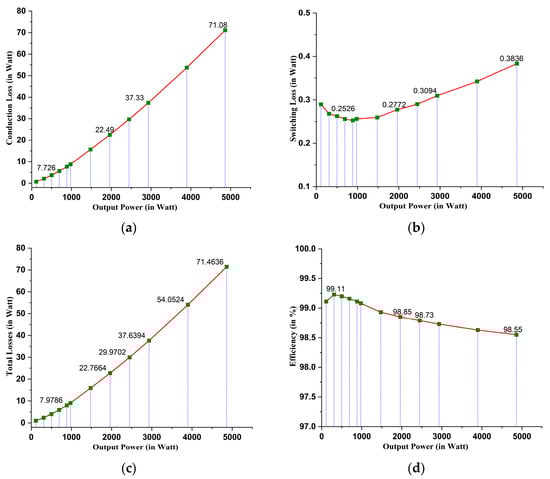
Figure 16.
Losses and efficiency at different output power levels: (a) conduction losses, (b) switching losses, (c) total losses, (d) efficiency.
Switching losses arise during the transition periods when the semiconductor switches turn ON and OFF. These losses are influenced by the switching frequency, the voltage and current during switching, and the characteristics of the switches. Switching losses are relatively small compared to conduction losses but still increase with output power, starting at 0.2897 W for 112.78 W output power and reaching 0.3836 W for 4861.54 W output power, as depicted in Figure 16b. Despite their smaller magnitude, switching losses contribute to the overall loss and can affect efficiency. The total loss, which is the sum of conduction and switching losses, increases as output power increases. Total loss starts at 1.0122 W for 112.78 W output power and increases to 71.4636 W for 4861 W output power. The increase in total losses is not linear but rather shows a steep rise as input power increases, especially beyond 1500 W input power. The total losses at different output power levels are depicted in Figure 16c.
The output power follows closely with the input power, but is always slightly less due to the losses. As expected, higher input power leads to higher output power, but the output power efficiency slightly decreases as output power increases. Efficiency at different output power levels is depicted in Figure 16d. The inverter is highly efficient at lower input powers, with efficiency slightly decreasing as input power increases. Conduction losses dominate the overall losses, and both conduction and switching losses increase with output power.
5. Conclusions
In this paper, a new structure of a 25-level inverter is conciliated from the perspective of reducing total power components and helping generate more voltage levels. The structure makes cascading connections with various voltage determination algorithms, portraying its merits in synthesizing higher voltage levels with reduced power components. Simulations of output voltage and load current at different MIs for different load conditions are carried out and experimentally verified. The values of THD at different MIs for the proposed MLI have been presented in this paper. The results from simulations and experimental studies can prove its capabilities in renewable energy applications.
Author Contributions
Methodology, B.M.; Software, K.K.M.; Formal analysis, D.D. and M.M.; Investigation, P.D.; Resources, M.M., G.F. and V.V.; Data curation, B.C.; Writing—review & editing, H.J. and B.C.; Supervision, G.F. and B.M. All authors have read and agreed to the published version of the manuscript.
Funding
This research received no external funding.
Data Availability Statement
The data presented in this study are available in this article.
Conflicts of Interest
The authors declare no conflict of interest.
References
- Chen, M.; Gao, C.; Yin, C.; Loh, P.C. Novel Cascaded Seven-Level Inverter with Embedded Voltage Boosting for Renewable Energy Applications. CPSS Trans. Power Electron. Appl. 2022, 7, 58–70. [Google Scholar] [CrossRef]
- Mondol, H.; Biswas, S.P.; Islam, R.; Mahfuz-Ur-Rahman, A.M.; Muttaqi, K.M. A New Hybrid Multilevel Inverter Topology with Level Shifted Multi-carrier PWM Technique for Harvesting Renewable Energy. In Proceedings of the 2020 IEEE Industry Applications Society Annual Meeting, Detroit, MI, USA, 10–16 October 2020; pp. 2574–2585. [Google Scholar] [CrossRef]
- Reddi, N.K.; Ramteke, M.R.; Suryawanshi, H.M.; Kothapalli, K.; Gawande, S.P. An Isolated Multi-Input ZCS DC–DC Front-End-Converter Based Multilevel Inverter for the Integration of Renewable Energy Sources. IEEE Trans. Ind. Appl. 2018, 54, 494–504. [Google Scholar] [CrossRef]
- Balachandran, A.; Jonsson, T.; Eriksson, L. Design and Analysis of Battery-Integrated Modular Multilevel Converters for Automotive Powertrain Applications. In Proceedings of the 2021 23rd European Conference on Power Electronics and Applications (EPE’21 ECCE Europe), Ghent, Belgium, 6–10 September 2021; pp. 1–12. [Google Scholar] [CrossRef]
- Khoucha, F.; Lagoun, S.M.; Marouani, K.; Kheloui, A.; Benbouzid, M.E.H. Hybrid Cascaded H-Bridge Multilevel-Inverter Induction-Motor-Drive Direct Torque Control for Automotive Applications. IEEE Trans. Ind. Electron. 2010, 57, 892–899. [Google Scholar] [CrossRef]
- Modeer, T.; Pallo, N.; Foulkes, T.; Barth, C.B.; Playa-Podgurski, R.C.N. Design of a GaN-Based Interleaved Nine-Level Flying Capacitor Multilevel Inverter for Electric Aircraft Applications. IEEE Trans. Power Electron. 2020, 35, 12153–12165. [Google Scholar] [CrossRef]
- Mahto, K.K.; Mahato, B.; Chandan, D.; Das, P.; Das, G.; Fotis, M. Mann. A New Symmetrical Source-Based DC/AC Converter with Experimental. Verification. Electron. 2024, 13, 1975. [Google Scholar] [CrossRef]
- Chen, W.L.; Su, Y.H. Negative Sequence Active and Reactive Currents Compensation for Unbalanced Three-Phase Networks Subject to Various Line Impedance Attributes. IEEE J. Emerg. Sel. Top. Power Electron. 2022, 10, 2528–2538. [Google Scholar] [CrossRef]
- Yadav, D.; Singh, N.; Bhadoria, V.; Vita, V.; Fotis, G.; Tsampasis, E.G.; Maris, T.I. Analysis of the Factors Influencing the 300 Performance of Single- and Multi-Diode PV Solar Modules. IEEE Access 2023, 11, 95507–95525. [Google Scholar] [CrossRef]
- Maris, T.I.; Kourtesi, S.; Ekonomou, L.; Fotis, G. Modeling of a single-phase photovoltaic inverter. Sol. Energy Mater. Sol. Cells 2007, 91, 1713–1725. [Google Scholar] [CrossRef]
- Ponnusamy, P.; Sivaraman, P.; Almakhles, D.J.; Padmanaban, S.; Leonowicz, Z.; Alagu, M.; Ali, J.S.M. A New Multilevel Inverter Topology with Reduced Power Components for Domestic Solar PV. Appl. IEEE Access 2020, 8, 187483–187497. [Google Scholar] [CrossRef]
- Bughneda, A.; Salem, M.; Richelli, A.; Ishak, D.; Alatai, S. Review of multilevel inverters for PV energy system applications. Energies 2021, 14, 1585. [Google Scholar] [CrossRef]
- Mahato, B.; Majumdar, S.; Jana, K.C. Carrier-based PWM techniques for multi-level inverters: A comprehensive performance study. Gazi Univ. J. Sci. Part. A Eng. Innov. 2018, 5, 101–111. [Google Scholar]
- Hosseinzadeh, M.A.; Sarebanzadeh, M.; Garcia, C.F.; Babaei, E.; Rodriguez, J.; Kennel, R. Reduced Multisource Switched-Capacitor Multilevel Inverter Topologies. IEEE Trans. Power Electron. 2022, 37, 14647–14666. [Google Scholar] [CrossRef]
- Chamarthi, P.K.; Agarwal, V.; Meutas, M.S.E.; Khadkakar, V. Novel 1–0 Dual Input Nine-Level Inverter Topology with Generalized Modulation Technique. IEEE Trans. Energy Convers. 2022, 37, 1789–1802. [Google Scholar] [CrossRef]
- Sadanala, C.; Pattoaik, S.P.; Singh, V.P. A novel switched capacitor based multilevel inverter with symmetrical and asymmetrical configurations. Electr. Eng. 2021, 103, 1461–1472. [Google Scholar] [CrossRef]
- Darmian, S.Y.; Barakati, S.M. A New Asymmetric Multilevel Inverter with Reduced Number of Components. IEEE J. Emerg. Sel. Top. Power Electron. 2020, 8, 4333–4342. [Google Scholar] [CrossRef]
- Pradeep, J.; Vengadakrishnan, K.; Palani, A.; Sandirasegarane, T. A new tri- source symmetric cascaded multilevel inverter topology with reduced power components. Circuit World 2022, 49, 431–444. [Google Scholar] [CrossRef]
- Chandrasekaran, K.; Mohanty, N.K.; Ranganathan, S. A new tapped sources stack succored modified HX bridge MLI Circuit World. Circuit World 2021, 47, 164–172. [Google Scholar] [CrossRef]
- Mahato, B.; Majumdar, S.; Jana, K.C. A new and generalized MLI with overall lesser power electronic devices. J. Circuits Syst. Comput. 2019, 29, 2050058. [Google Scholar] [CrossRef]
- Paul, S.; Mahato, B.; Majumdar, S.; Jana, K.C. A Novel H-Type MLI with the reduction in Power Electronic Devices. In Proceedings of the 2021 12th Power Electronics, Drive Systems, and Technologies Conference (PEDSTC), Tabriz, Iran, 2–4 February 2021; pp. 1–5. [Google Scholar] [CrossRef]
- Tupakula, R.R. A generalized single-phase cascaded multilevel inverter with reduced switch count. Electr. Eng. 2021, 103, 1115–1125. [Google Scholar] [CrossRef]
- Khasm, S.R.; Dhaminyslu, C. Design and Implementation of Asymmetrical Multilevel Inverter with Reduced Components and Low Voltage Stress. IEEE Access 2022, 10, 3495–3511. [Google Scholar] [CrossRef]
- Babaei, E.; Hosseinzadeh, M.A.; Sarbanzadeh, M.; Cecati, C. A new basic unit for cascaded multilevel inverters with reduced number of power electronic devices. In Proceedings of the 2016 7th Power Electronics and Drive Systems Technologies Conference (PEDSTC), Tehran, Iran, 16–18 February2016; pp. 185–190. [Google Scholar] [CrossRef]
- Harbi, I.A.; Azazi, H.Z.; Lashing, A.E.; Elsabbe, A. A higher levels multilevel inverter with reduced number of switches. Int. J. Electron. 2020, 105, 1286–1299. [Google Scholar] [CrossRef]
- Kannan, C.; Mohanty, N.K. A Non-modular Matrix Structure for Component Count Waning in Multilevel Inversion. Electr. Eng. Technol. 2022, 17, 251–259. [Google Scholar] [CrossRef]
- Mahato, B.; Majumdar, S.; Jana, K.C.; Babaei, E.; Mohanta, D.K. A new switch-diode cell-based single-phase cascaded multilevel inverter. Soft Comput. 2023, 27, 13719–13738. [Google Scholar] [CrossRef]
- Mahato, B.; Majumdar, S.; Paul, S.; Pal, P.K.; Jana, K.C. A new and modular back-to-back connected T-type inverter for minimum number of power devices, TSV, and cost factor. IETE Tech. Rev. 2022, 39, 357–374. [Google Scholar] [CrossRef]
- Mahato, B.; Ranjan, M.; Pal, P.K.; Gupta, S.K.; Mahto, K.M. Design, development and verification of a new multilevel inverter for reduced power switches. Arch. Electr. Eng. 2022, 1051–1063. [Google Scholar] [CrossRef]
- Mahato, B.; Majumdar, S.; Jana, K.C.; Thakura, P.R.; Mohanta, D.K. Experimental verification of a new scheme of MLI based on modified T-type inverter and switched-diode cell with lower number of circuit devices. Electr. Power Compon. Syst. 2021, 48, 1814–1834. [Google Scholar] [CrossRef]
- Mahato, B.; Majumdar, S.; Jana, K.C. Reduction of power electronic devices in a single-phase generalized multilevel inverter. J. Circuits Syst. Comput. 2020, 2050093. [Google Scholar] [CrossRef]
- Majumdar, S.; Mahato, B.; Jana, K.C. Optimum structure-based multi-level inverter with doubling circuit configuration. J. Circuits Syst. Comput. 2019, 1950194. [Google Scholar] [CrossRef]
- Chandrasekaran, K.; Mohanty, N.K. A Flexible Rung Ladder Structured Multilevel Inverter. Tech. Gaz. 2020, 27, 1044–1049. [Google Scholar] [CrossRef]
Disclaimer/Publisher’s Note: The statements, opinions and data contained in all publications are solely those of the individual author(s) and contributor(s) and not of MDPI and/or the editor(s). MDPI and/or the editor(s) disclaim responsibility for any injury to people or property resulting from any ideas, methods, instructions or products referred to in the content. |
© 2024 by the authors. Licensee MDPI, Basel, Switzerland. This article is an open access article distributed under the terms and conditions of the Creative Commons Attribution (CC BY) license (https://creativecommons.org/licenses/by/4.0/).