Abstract
Enhanced class E inverters (EFn or E/Fn) reduce the high peak switch voltage that is prevalent in class E inverters. Additionally, their stability and load regulation capabilities are improved as compared to class E inverters. This paper proposes an enhanced class E inverter (E/F3) with a piezoelectric transformer (PT) replacing the auxiliary resonant networks. This class E/F3 inverter is designed by adding a tuned auxiliary LC network at the third harmonic of the switching frequency to the class E inverter. Both the primary and auxiliary resonant networks are realized using a piezoelectric transformer (PT). The converter is simulated in LTspice and an experimental prototype is built and tested. It is found that the experimental results concur with the simulation results, with a measured efficiency of 90%. Thus, the theoretical design is verified and the concept of energy extraction is achieved.
1. Introduction
The compact architecture of class E inverters, which has a low component count and a simultaneous high power transmission capability, is largely responsible for their popularity. Additionally, if combined with zero voltage switching (ZVS) or zero derivative voltage switching (ZVDS) approaches, they can function at very high switching frequencies with excellent efficiency. The ZVS/ZVDS class E inverters’ analyses and modeling have been thoroughly documented in the literature [1,2,3]. This architecture does have one significant drawback, though. This is seriously concerning, because the peak switch voltage is so large (3.5 to 5 times, depending on the duty ratio) [4,5,6,7,8]. The upgraded class E configurations are suggested, among other things, to address this problem, and the LC networks are tuned at the nth harmonic of the switching frequency [9,10,11,12,13,14,15,16,17,18]. In this paper, a class E/F3 inverter is designed. The inverter’s topology is shown in Figure 1a. A piezoelectric transformer (PT-T1PP0361) is used for energy extraction in the primary and auxiliary resonant networks. This PT is shown in Figure 1b, along with its mason equivalent circuit being demonstrated in Figure 1c. In Figure 1a, the inverter has primary and secondary resonant networks tuned at different resonant frequencies. In this design, either the primary or secondary resonant network is replaced by the PT, or the PT is used to realize the other network using conventional magnetic components. The experimental prototype is constructed and put through testing, while the inverter is simulated in LTSPICE utilizing a PT emulation circuit. The following sections provide details on the testing’s design and outcomes. In Section 2, the circuit configuration and modes of operation are described. In Section 3, the circuit design is explained. In Section 4, the simulation and experimental verification process is described. Section 5 concludes the paper.
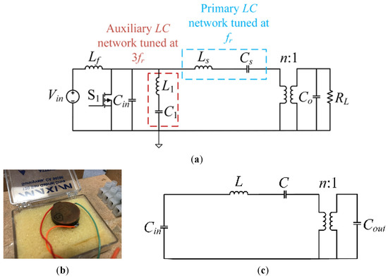
Figure 1.
(a) The class E/F3 topology with primary and auxiliary resonant networks tuned at fr and 3fr, respectively. (b) The radial mode PT (T1PP0361). (c) The PT mason equivalent circuit.
2. The Circuit Configuration and Modes of Operation
In Figure 1a, the inductance Ls and capacitance Cs make up the primary resonant tank of the class E/F3 inverter, which resonates at a resonant frequency (fr) in accordance with a quality factor (Q). The input inductance (Lf) is designed to deliver an extremely low ripple current while maintaining a steady DC current. The input capacitance Cin absorbs the drain-to-source (non-linear) capacitance (Cds) of the switch. The auxiliary resonant branch consists of the auxiliary resonant inductance (L1) and capacitance (C1). The primary resonant frequency is fr, and the auxiliary resonant frequency is 3fr. The primary resonant frequency fr and the switching frequency fs are both chosen to be equal, or the fs is slightly higher than the fr. To accomplish the ZVS operation, the switch S1 is run at its optimal duty ratio Dopt. The switching pattern is depicted as follows.
When the switch S1 is ON in mode 1, the voltage across the capacitor Cin is forced to zero. The Lf is charged as the input current (Iin) passes through S1. The resonant current flows through the switch in the resonant tank, transferring the stored energy from the Cs to the Ls and completing one half of the resonant cycle. At the conclusion of this cycle, the energy transfer is completed and the current starts to decline. When S1 opens at θ = 2πD in mode 2, the Iin charges the input capacitor Cin, which eventually achieves the peak switch voltage (VS1,peak), before being discharged through the primary resonant tank. Due to the inductive nature of the load network in mode 2, the output current (Iout) lags the input voltage to the resonant tank (VS1) in mode 2. This ensures that the ZVS is operating for the designed inverter. On that note, the following conditions must be met to achieve ZVS or ZVDS,
In Figure 1b, the PT mason equivalent circuit replaces the primary or the secondary resonant tank in the class E/F3 resonant inverter.
3. Circuit Design
In this section, the circuit components are designed [7,8] according to the specifications that are stated in Table 1. As mentioned earlier, the primary and auxiliary resonant tank is replaced by the PT. The PT characteristic component values are measured using a Bode 100 Network Analyzer. The measured parameters are stated in Table 2.

Table 1.
Design specifications.
Table 2.
Characteristic component values of PT.
An input inductor Lf = 100 µH is selected for both designs involving the PT, as the primary or auxiliary resonant network.
- A.
- The PT as Primary Resonant Tank
In this subsection, the inverter is designed while the primary resonant tank is replaced by a PT. In Figure 2, the circuit diagram with the PT mason equivalent circuit is shown. In this case, as can be derived from Table 2, Ls = LPT = 4.86 mH, Cs = CPT = 0.814 nF, n ≈ 2.22, Cin = Cin−PT = 2.53 nF, and Co = Cout−PT = 4.58 nF. The LofCof filter is designed with a cutoff frequency of fc = 120 kHz. Alternatively, without the LofCof filter, a large output capacitor, Cof = 330 µH, can be used to reduce the high frequency harmonics, as shown in Figure 2b. As the PT replaces the primary resonant tank, the primary resonant frequency fr is 80 kHz. The auxiliary circuit has to resonate at fraux = 3fr. The components L1 and C1 are selected for Q = 0.707 from Table 1 and for RL = 100 Ω.
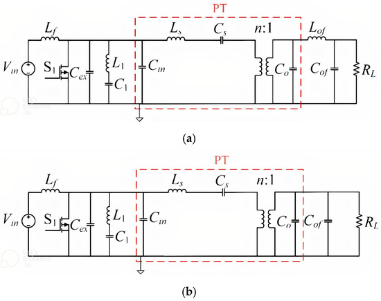
Figure 2.
PT as primary resonant tank, (a) with an output LC filter, and (b) with output filter capacitor (Cof).
As Cin−PT = 2.53 nF, an external input capacitance Cex = Cin − Cin−PT = (40.15 − 2.53)nF = 37.62 nF has to be added. Practically, Cex ≈ 47 nF is selected with consideration to its availability. The circuit parameters are stated in Table 3.
Table 3.
The circuit parameters with PT as primary resonant tank.
- B.
- The PT as Auxiliary Resonant Tank
In Figure 3, the circuit diagram, with the PT replacing the auxiliary resonant network, is shown. In this case, as can be derived from Table 2, L1 = LPT = 4.86 mH, C1 = CPT = 0.814 nF, n ≈ 2.22, and Cin = Cin−PT = 2.53 nF. For the structure of the PT, the Cout−pri comes in parallel to the C1. This is due to the PT output capacitance (Cout−PT) being reflected to the primary side and can be computed as:
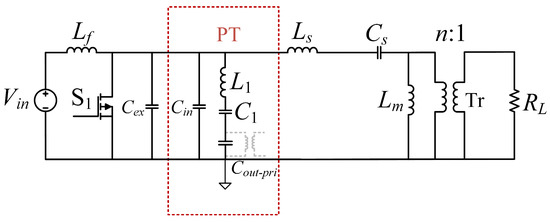
Figure 3.
The class E/F3 topology with PT as auxiliary resonant tank and magnetic transformer.
In (6), the required Cin is calculated. Hence, an external input capacitance, Cex ≈ 47 nF, is added to the required design. The magnetic transformer (Tr) has a magnetic inductance of Lm = 18 µH. The circuit parameters are stated in Table 4.
Table 4.
The circuit parameters with PT as auxiliary resonant tank.
4. Simulation and Experimental Verification
The class E/F3 inverter with the integrated PT is simulated in an LTSPICE simulation platform and prototypes are built. In Figure 4, the LTSPICE simulation circuit is shown. In this configuration, the PT emulator (i.e., the mason equivalent) replaces the primary resonant tank. The component design is presented in the previous section and utilizes a PT as the primary or auxiliary resonant network. In the rest of this section, the results for the simulation and experimentation of the designed inverter are presented and described. The experimental setup is shown in Figure 5.
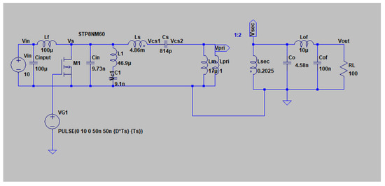
Figure 4.
Simulation circuit: the class E/F3 topology with PT as primary resonant tank.
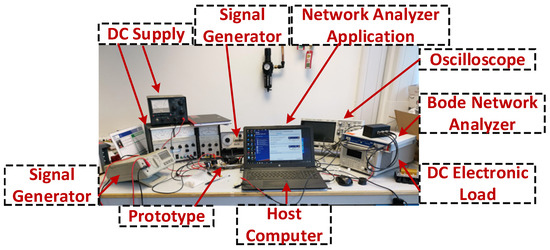
Figure 5.
Experimental setup.
- A.
- The PT as Primary Resonant Tank
In Figure 5, the LTSPICE simulation circuit is shown. In this configuration, the PT emulator (i.e., the mason equivalent) replaces the primary resonant tank.
In Figure 6a, the switch voltage from the LTSPICE simulation is demonstrated. As can be seen, the peak switch voltage is 34 V. From Figure 6b, it is obvious that the output voltage (Vout) is smooth and contains less harmonics. However, the reverse diode’s conduction shows that the inverter is not performing at its best. The inverter’s output power is determined as follows:
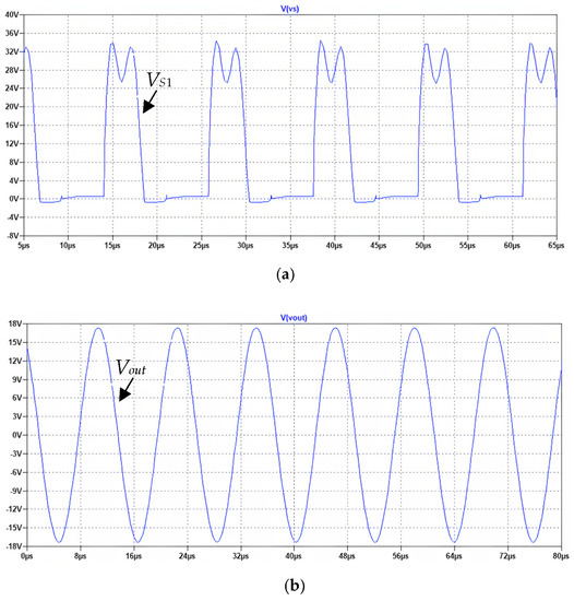
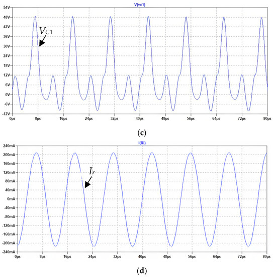
Figure 6.
Simulation results: the class E/F3 topology with PT as auxiliary resonant tank. (a) The switch voltage, (b) the output voltage, Vout (c) the auxiliary resonant capacitor voltage, VC1, and (d) the primary resonant current, Ir.
The experimental findings are shown in Figure 7. As can be seen, the switch’s reverse diode (S1) conducts for a brief length of time, achieving the ZVS/ZDS in the sub-optimal zone. This output power is determined as follows:
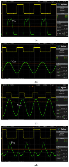
Figure 7.
Experimental results for class E/F3 topology with piezoelectric transformer as primary resonant tank. (a) The switch voltage, VS1, (b) the output voltage with LC output filter, Vout, (c) the output voltage with output filter capacitance, Vout, and (d) the auxiliary resonant capacitor voltage, VC1.
The high frequency harmonics in the Vout can be decreased using an LC low pass filter or an output capacitor, as shown in Figure 7b,c. Additionally, it is clear that the simulation and experimental results closely support the theoretical design. Table 5 compiles the findings to show how comparable they are.
Table 5.
The simulation and experimental prototype results.
- B.
- The PT as Auxiliary Resonant Tank
In Figure 8, the LTSPICE simulation circuit is shown for the PT that replaces the conventional auxiliary resonant network. In this configuration, the PT emulator (i.e., the mason equivalent) is used for simulation purposes.
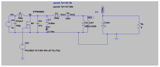
Figure 8.
Simulation circuit: the class E/F3 topology with PT as auxiliary resonant tank.
The simulation results are shown in Figure 9. The ZVS is attained, as seen by the switch voltage waveform in Figure 9b. However, the reverse diode’s conduction also suggests that the converter is not performing at its best.
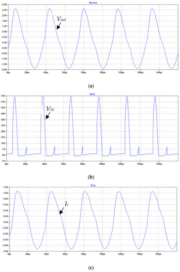
Figure 9.
Simulation results for class E/F3 topology with PT as auxiliary resonant tank. (a) The output voltage, Vout, (b) the switch voltage, VS1, and (c) The primary resonant current, Ir.
The experimental findings for the PT working as an auxiliary resonant tank are shown in Figure 10. It is clear from Figure 10a that a higher harmonic content dominates the output voltage (Vout). To get rid of the higher frequency harmonics, a 100 kHz output low pass filter can be used. Additionally, the ZVS is attained in the sub-optimal region, as seen in Figure 9b and Figure 10b. It should be noticed that the peak switch voltage (VS1,peak) is still high, despite employing the auxiliary network (i.e., the PT). By increasing the capacitance ratio k, this high switch peak voltage can be reduced. However, the latter necessitates the use of a different PT, which is not executed in this work because of the non-availability of the required PT. Nevertheless, the idea of utilizing a PT for the energy extraction in a class E/F3 inverter is confirmed. In Figure 11, the power versus the efficiency (η) curve is shown. The efficiency is measured under the specified conditions, as described in Table 1. As observed, the converter operates at approximately 90%, while the output power (Pout) is 5 W or lower. Overall, the simulation and experimental results are shown in Table 5. It can be observed that the results are quite consistent with one another and conform to the theoretical design. The slight differences in the results are due to the deviations of the parametric values of the PT equivalent circuit at a high frequency.
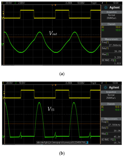
Figure 10.
Experimental results for class E/F3 topology with PT as primary resonant tank. (a) The output voltage, Vout, and (b) the switch voltage, VS1.
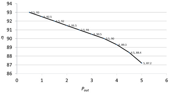
Figure 11.
The output power (Pout) versus measured efficiency (η).
5. Conclusions
In this paper, the primary or auxiliary resonant tank is replaced with a PT in a class E/F3 inverter. According to the circuit analysis, this inverter can be used in ZVS mode while the PT replaces the traditional resonant tanks. The inverter is simulated in LTspice and an experimental prototype of the inverter is tested. The simulation and experimental results are consistent with one another, indicating the validity of the theoretical design. Additionally, by raising the value of k, the inverter’s peak switch voltage in the class E/F3 can be further reduced, which remains a future scope for this work. A compact and low-power inverter can be realized by replacing its traditional magnetic components with a PT. This concept is also applicable for other enhanced class E inverters. However, there are opportunities for further investigation into this topic.
Author Contributions
Conceptualization, R.H.A. and M.H.M.; methodology, R.H.A., M.S.B.A. and A.S.; validation, R.H.A., A.S. and M.H.M.; formal analysis, A.S.; investigation, R.H.A. and M.H.M.; resources, R.H.A.; data curation, R.H.A. and A.A.M.; writing—original, R.H.A., A.R.B. and A.S.; writing—review and editing, R.H.A. and M.S.B.A.; visualization, R.H.A. and M.H.M.; supervision, R.H.A. All authors have read and agreed to the published version of the manuscript.
Funding
This research received no external funding.
Conflicts of Interest
The authors declare no conflict of interest.
Nomenclature
| fs | Switching frequency |
| fr | Resonant frequency |
| Vin | Input voltage |
| Vout | Output voltage |
| VS1 | Switch voltage |
| Iin | Input current |
| Iout | Output current |
| Pin | Input power |
| Pout | Output power |
| Ls | Primary inductance |
| Cs | Primary capacitance |
| L1 | Auxiliary inductance |
| C1 | Auxiliary capacitance |
| Cr | Resonant capacitance |
| Cout | Output capacitance |
| RL | Load resistance |
| k | Capacitance ratio |
| Cin−PT | PT equivalent input capacitance |
| Cout−PT | PT equivalent output capacitance |
| ZVS | Zero Voltage Switching |
| ZVDS | Zero Voltage Derivative Switching |
| E/F3 | Class E/F3 Inverter |
References
- Huang, J.; Zhang, X.; Li, Y.; Li, Q. A novel ZVS class E/F3 inverter with piezoelectric transformer for energy harvesting. IEEE Trans. Ind. Electron. 2021, 68, 400–408. [Google Scholar] [CrossRef]
- Islam, M.M.; Islam, M.A.; Faruque, M.R.I. ZVS Class E/F3 Inverter Using Piezoelectric Transformer for Wireless Power Transfer. IEEE Trans. Circuits Syst. II Express Briefs 2021, 68, 1421–1425. [Google Scholar] [CrossRef]
- Lin, H.; Zhu, J.; Jiao, J.; He, X. Design and implementation of a ZVS class E/F3 inverter with piezoelectric transformer for wireless power transfer. IEEE Trans. Ind. Electron. 2020, 67, 1182–1192. [Google Scholar] [CrossRef]
- Hayati, M.; Lotfi, A.; Kazimierczuk, M.K.; Sekiya, H. Analysis and Design of Class-E Power Amplifier With MOSFET Parasitic Linear and Nonlinear Capacitances at Any Duty Ratio. IEEE Trans. Power Electron. 2013, 28, 5222–5232. [Google Scholar] [CrossRef]
- Kessler, D.J.; Kazimierczuk, M.K. Power losses and efficiency of class-E power amplifier at any duty ratio. IEEE Trans. Circuits Syst. I Regul. Pap. 2004, 51, 1675–1689. [Google Scholar] [CrossRef]
- Shigeno, A.; Shimizu, T.; Koizumi, H. Current-source parallel resonant class E inverter with low peak switch current. In Proceedings of the IECON 2017—43rd Annual Conference of the IEEE Industrial Electronics Society, Beijing, China, 29 October–1 November 2017; pp. 5330–5335. [Google Scholar]
- Kaczmarczyk, Z. High-Efficiency Class E, EF2, and E/F3 Inverters. IEEE Trans. Ind. Electron. 2006, 53, 1584–1593. [Google Scholar] [CrossRef]
- Ayachit, A.; Corti, F.; Reatti, A.; Kazimierczuk, M. Zero-Voltage Switching Operation of Transformer Class-E Inverter at Any Coupling Coefficient. IEEE Trans. Ind. Electron. 2018, 66, 1809–1919. [Google Scholar] [CrossRef]
- Kaczmarczyk, Z.; Jurczak, W. A Push–Pull Class-E Inverter With Improved Efficiency. IEEE Trans. Ind. Electron. 2008, 55, 1871–1874. [Google Scholar] [CrossRef]
- Kazimierczuk, M.K.; Jozwik, J. DC/DC converter with class E zero-voltage-switching inverter and class E zero-current-switching rectifier. IEEE Trans. Circuits Syst. 1989, 36, 1485–1488. [Google Scholar] [CrossRef]
- Li, Y.; Sue, S. Exactly analysis of ZVS behavior for class E inverter with resonant components varying. In Proceedings of the 2011 6th IEEE Conference on Industrial Electronics and Applications, Beijing, China, 21–23 June 2011; pp. 1245–1250. [Google Scholar]
- Kee, S.D.; Aoki, I.; Hajimiri, A.; Rutledge, D. The class-E/F family of ZVS switching amplifiers. IEEE Trans. Microw. Theory Tech. 2003, 51, 1677–1690. [Google Scholar] [CrossRef]
- Grebennikov, A. High-efficiency class E/F lumped and transmission-line power amplifiers. IEEE Trans. Microw. Theory Tech. 2011, 59, 1579–1588. [Google Scholar] [CrossRef]
- Rivas, J.M.; Han, Y.; Leitermann, O.; Sagneri, A.D.; Perreault, D.J. A High-Frequency Resonant Inverter Topology With Low-Voltage Stress. IEEE Trans. Power Electron. 2008, 23, 1759–1771. [Google Scholar] [CrossRef]
- Aldhaher, S.; Yates, D.C.; Mitcheson, P.D. Modeling and Analysis of Class EF and Class E/F Inverters With Series-Tuned Resonant Networks. IEEE Trans. Power Electron. 2016, 31, 3415–3430. [Google Scholar] [CrossRef]
- You, F.; He, S.; Tang, X.; Deng, X. High-Efficiency Single-Ended Class-EF2 Power Amplifier With Finite DC Feed Inductor. IEEE Trans. Microw. Theory Tech. 2009, 58, 32–40. [Google Scholar]
- Grebennikov, A. Load network design techniques for class E RF and microwave amplifiers. High Freq. Electron. 2004, 3, 18–32. [Google Scholar]
- Grebennikov, A. High-efficiency class-FE tuned power amplifiers. IEEE Trans. Circuits Syst. I Regul. Pap. 2008, 55, 3284–3292. [Google Scholar] [CrossRef]
Disclaimer/Publisher’s Note: The statements, opinions and data contained in all publications are solely those of the individual author(s) and contributor(s) and not of MDPI and/or the editor(s). MDPI and/or the editor(s) disclaim responsibility for any injury to people or property resulting from any ideas, methods, instructions or products referred to in the content. |
© 2023 by the authors. Licensee MDPI, Basel, Switzerland. This article is an open access article distributed under the terms and conditions of the Creative Commons Attribution (CC BY) license (https://creativecommons.org/licenses/by/4.0/).