
The ZVS Class E/F3 Inverter Using Piezoelectric Transformers for Energy Extraction

 ,
,  ,
,  ,
,  , and
, and 
Abstract
1. Introduction
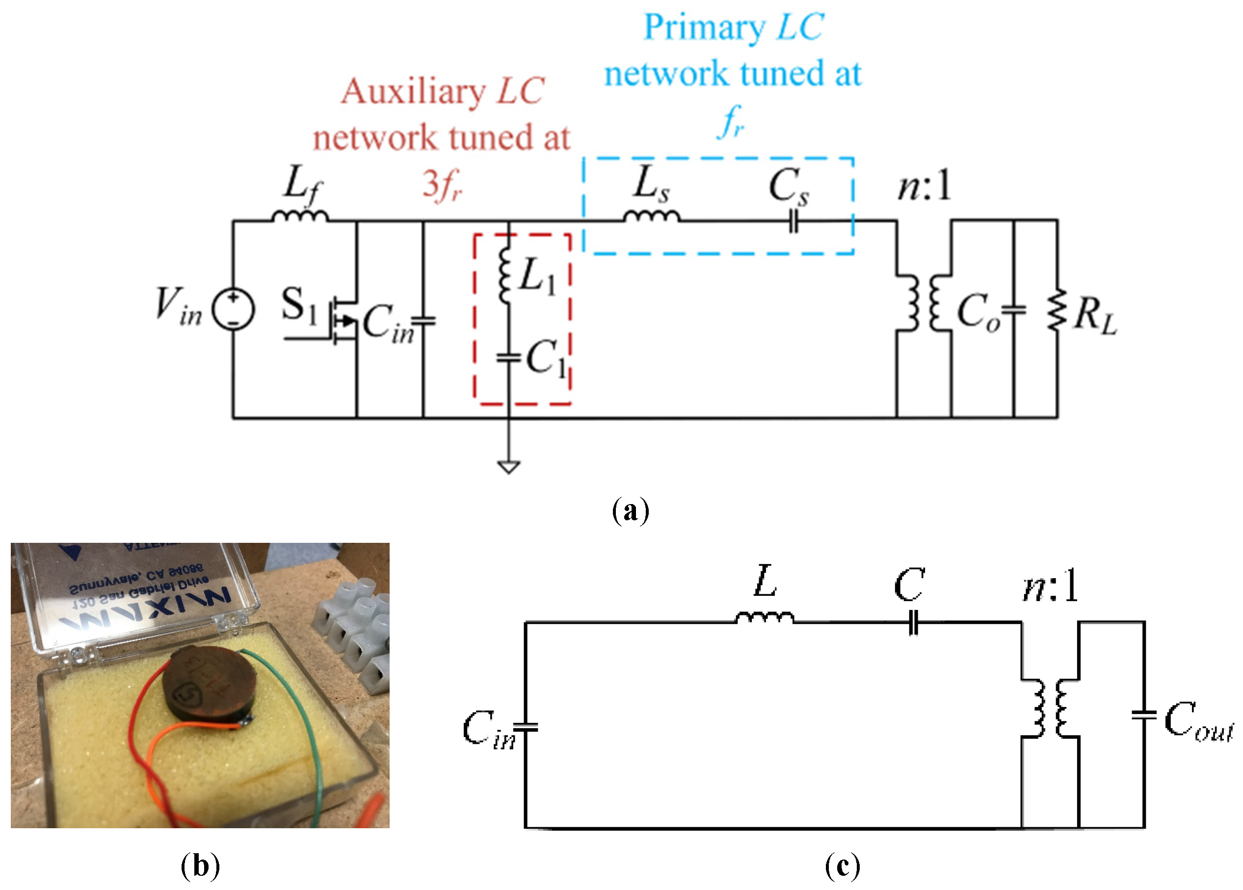
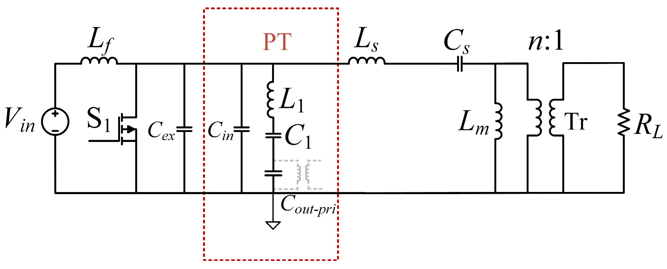
2. The Circuit Configuration and Modes of Operation
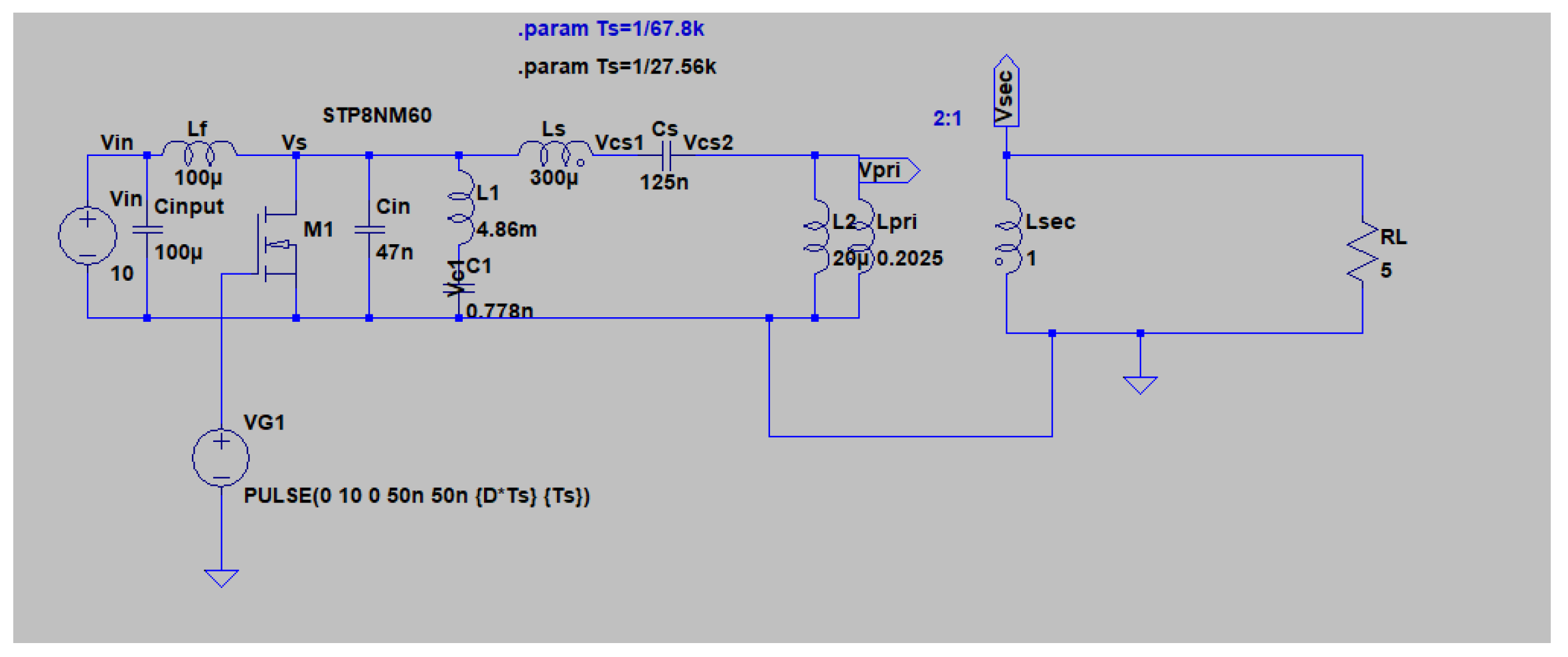
3. Circuit Design
- A.
- The PT as Primary Resonant Tank
- B.
- The PT as Auxiliary Resonant Tank
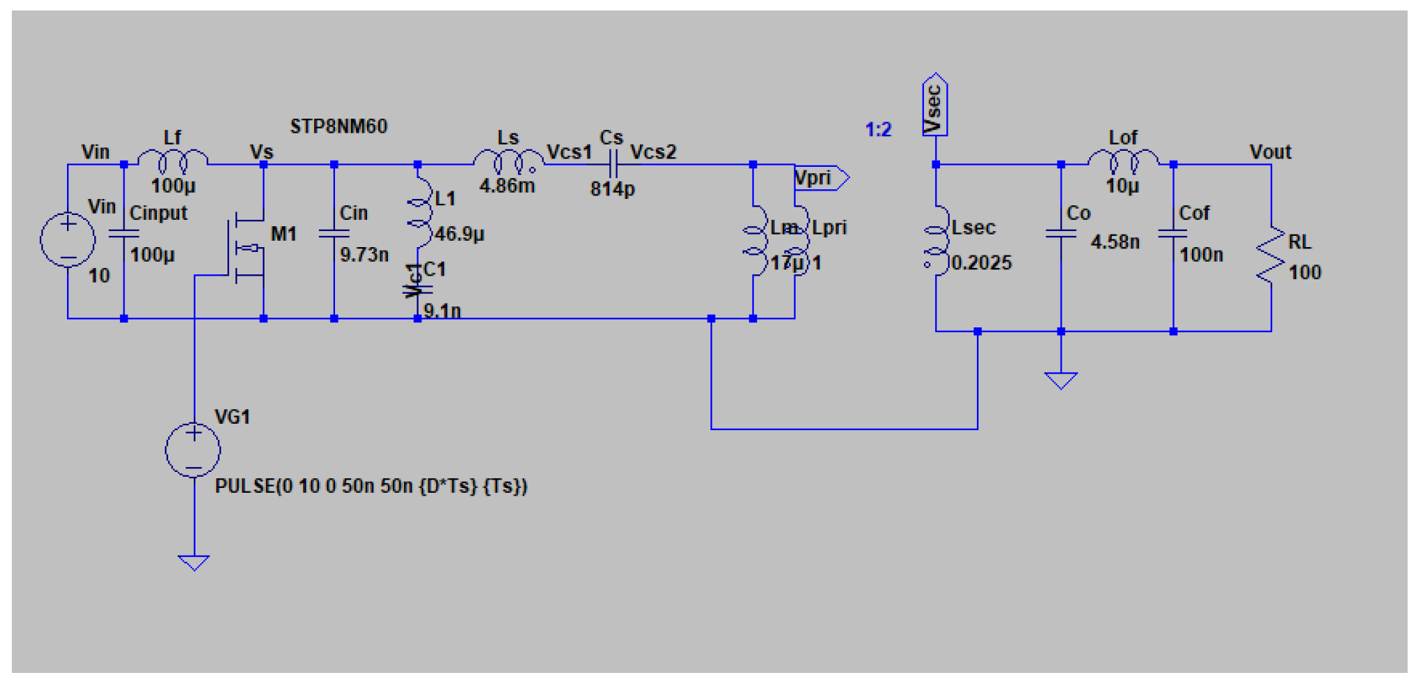
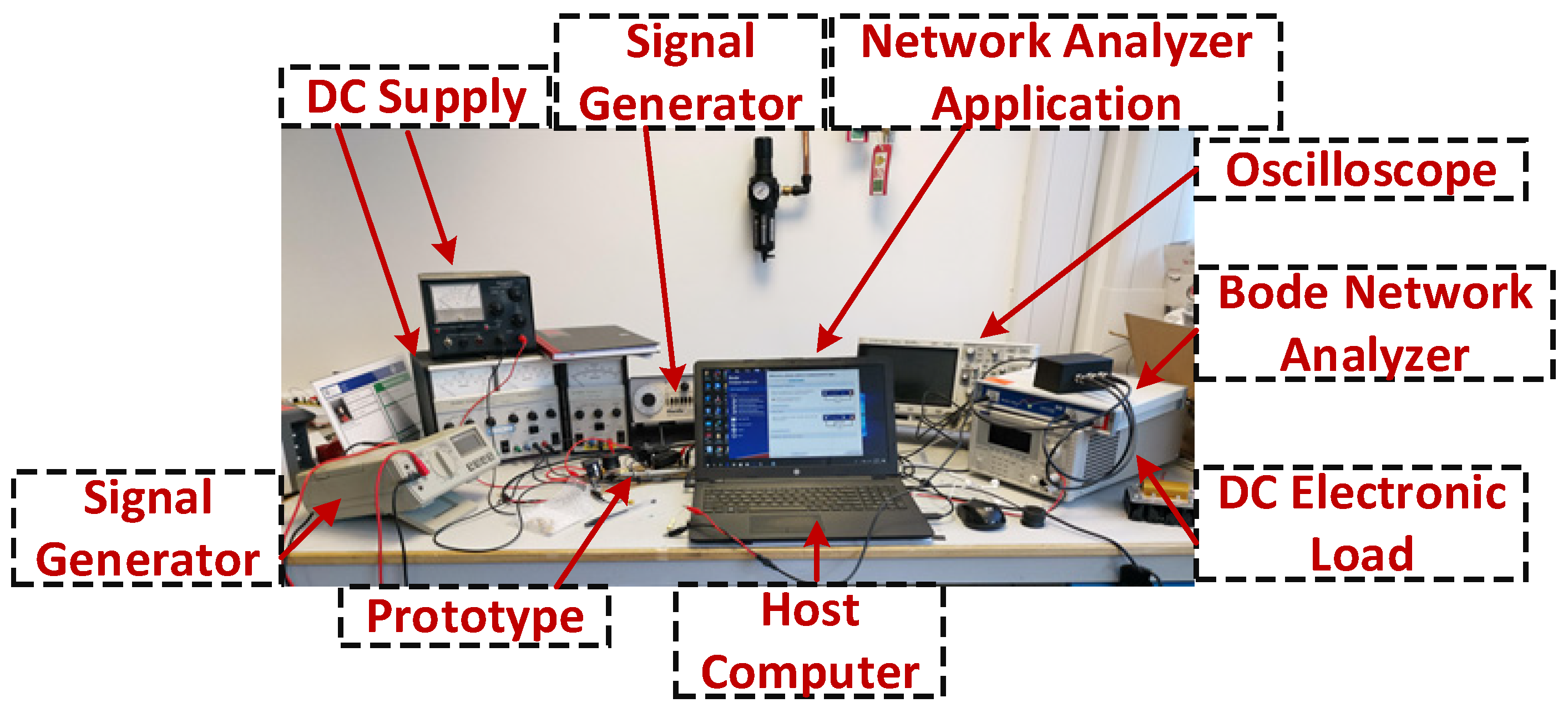
4. Simulation and Experimental Verification
- A.
- The PT as Primary Resonant Tank
- B.
- The PT as Auxiliary Resonant Tank
5. Conclusions
Author Contributions
Funding
Conflicts of Interest
Nomenclature
| fs | Switching frequency |
| fr | Resonant frequency |
| Vin | Input voltage |
| Vout | Output voltage |
| VS1 | Switch voltage |
| Iin | Input current |
| Iout | Output current |
| Pin | Input power |
| Pout | Output power |
| Ls | Primary inductance |
| Cs | Primary capacitance |
| L1 | Auxiliary inductance |
| C1 | Auxiliary capacitance |
| Cr | Resonant capacitance |
| Cout | Output capacitance |
| RL | Load resistance |
| k | Capacitance ratio |
| Cin−PT | PT equivalent input capacitance |
| Cout−PT | PT equivalent output capacitance |
| ZVS | Zero Voltage Switching |
| ZVDS | Zero Voltage Derivative Switching |
| E/F3 | Class E/F3 Inverter |
References
- Huang, J.; Zhang, X.; Li, Y.; Li, Q. A novel ZVS class E/F3 inverter with piezoelectric transformer for energy harvesting. IEEE Trans. Ind. Electron. 2021, 68, 400–408. [Google Scholar] [CrossRef]
- Islam, M.M.; Islam, M.A.; Faruque, M.R.I. ZVS Class E/F3 Inverter Using Piezoelectric Transformer for Wireless Power Transfer. IEEE Trans. Circuits Syst. II Express Briefs 2021, 68, 1421–1425. [Google Scholar] [CrossRef]
- Lin, H.; Zhu, J.; Jiao, J.; He, X. Design and implementation of a ZVS class E/F3 inverter with piezoelectric transformer for wireless power transfer. IEEE Trans. Ind. Electron. 2020, 67, 1182–1192. [Google Scholar] [CrossRef]
- Hayati, M.; Lotfi, A.; Kazimierczuk, M.K.; Sekiya, H. Analysis and Design of Class-E Power Amplifier With MOSFET Parasitic Linear and Nonlinear Capacitances at Any Duty Ratio. IEEE Trans. Power Electron. 2013, 28, 5222–5232. [Google Scholar] [CrossRef]
- Kessler, D.J.; Kazimierczuk, M.K. Power losses and efficiency of class-E power amplifier at any duty ratio. IEEE Trans. Circuits Syst. I Regul. Pap. 2004, 51, 1675–1689. [Google Scholar] [CrossRef]
- Shigeno, A.; Shimizu, T.; Koizumi, H. Current-source parallel resonant class E inverter with low peak switch current. In Proceedings of the IECON 2017—43rd Annual Conference of the IEEE Industrial Electronics Society, Beijing, China, 29 October–1 November 2017; pp. 5330–5335. [Google Scholar]
- Kaczmarczyk, Z. High-Efficiency Class E, EF2, and E/F3 Inverters. IEEE Trans. Ind. Electron. 2006, 53, 1584–1593. [Google Scholar] [CrossRef]
- Ayachit, A.; Corti, F.; Reatti, A.; Kazimierczuk, M. Zero-Voltage Switching Operation of Transformer Class-E Inverter at Any Coupling Coefficient. IEEE Trans. Ind. Electron. 2018, 66, 1809–1919. [Google Scholar] [CrossRef]
- Kaczmarczyk, Z.; Jurczak, W. A Push–Pull Class-E Inverter With Improved Efficiency. IEEE Trans. Ind. Electron. 2008, 55, 1871–1874. [Google Scholar] [CrossRef]
- Kazimierczuk, M.K.; Jozwik, J. DC/DC converter with class E zero-voltage-switching inverter and class E zero-current-switching rectifier. IEEE Trans. Circuits Syst. 1989, 36, 1485–1488. [Google Scholar] [CrossRef]
- Li, Y.; Sue, S. Exactly analysis of ZVS behavior for class E inverter with resonant components varying. In Proceedings of the 2011 6th IEEE Conference on Industrial Electronics and Applications, Beijing, China, 21–23 June 2011; pp. 1245–1250. [Google Scholar]
- Kee, S.D.; Aoki, I.; Hajimiri, A.; Rutledge, D. The class-E/F family of ZVS switching amplifiers. IEEE Trans. Microw. Theory Tech. 2003, 51, 1677–1690. [Google Scholar] [CrossRef]
- Grebennikov, A. High-efficiency class E/F lumped and transmission-line power amplifiers. IEEE Trans. Microw. Theory Tech. 2011, 59, 1579–1588. [Google Scholar] [CrossRef]
- Rivas, J.M.; Han, Y.; Leitermann, O.; Sagneri, A.D.; Perreault, D.J. A High-Frequency Resonant Inverter Topology With Low-Voltage Stress. IEEE Trans. Power Electron. 2008, 23, 1759–1771. [Google Scholar] [CrossRef]
- Aldhaher, S.; Yates, D.C.; Mitcheson, P.D. Modeling and Analysis of Class EF and Class E/F Inverters With Series-Tuned Resonant Networks. IEEE Trans. Power Electron. 2016, 31, 3415–3430. [Google Scholar] [CrossRef]
- You, F.; He, S.; Tang, X.; Deng, X. High-Efficiency Single-Ended Class-EF2 Power Amplifier With Finite DC Feed Inductor. IEEE Trans. Microw. Theory Tech. 2009, 58, 32–40. [Google Scholar]
- Grebennikov, A. Load network design techniques for class E RF and microwave amplifiers. High Freq. Electron. 2004, 3, 18–32. [Google Scholar]
- Grebennikov, A. High-efficiency class-FE tuned power amplifiers. IEEE Trans. Circuits Syst. I Regul. Pap. 2008, 55, 3284–3292. [Google Scholar] [CrossRef]


| Parameters | Symbols | Values |
|---|---|---|
| Input voltage | Vin | 10 V |
| Primary resonant frequency | fr | 26.67 kHz |
| Auxiliary resonant frequency | 3fr | 80 kHz |
| Capacitance ratio | k (C1/Cin) | 10 |
| Quality factor of the conventional resonant tank | Qaux | 0.707 |
| Parameter | Symbol | Value |
|---|---|---|
| Series resistance | RPT | 8.69 Ω |
| Resonant inductor | LS | 4.86 mH |
| Resonant capacitor | CS | 0.814 nF |
| Input capacitor | Cin | 2.53 nF |
| Output capacitor | Co | 4.58 nF |
| Turns ratio | n:1 | 1:0.45 |
| Quality factor of the PT | QPT | 281.30 |
| Parameter | Values | |
|---|---|---|
| PT input capacitance | Cin | 2.53 nF |
| External input capacitance | Cex | 47 nF |
| PT output capacitance | Co | 4.70 nF |
| PT transformer ratio | n | ≈2.22 |
| Load resistance | RL | 100 Ω |
| Primary resonant inductance | Ls | 4.77 mH |
| Primary resonant capacitance | Cs | 814 pF |
| Auxiliary resonant inductance | L1 | 46.90 µH |
| Auxiliary resonant capacitance | C1 | 9.10 nF |
| Output filter inductor | Lof | 200 µH |
| Output filter capacitance | Cof | 100 nF |
| Parameter | Values | |
|---|---|---|
| PT input capacitance | Cin−PT | 2.53 nF |
| External input capacitance | Cex | 47 nF |
| PT output capacitance | Cout−PT | 4.57 nF |
| Transformer ratio | n:1 | 2:1 |
| Load resistance | RL | 100 Ω |
| PT auxiliary resonant inductance | L1 | 4.86 mH |
| PT auxiliary resonant capacitance | C1 | 814 pF |
| PT output capacitance | Cout−pri (n2 ∗ Cout−PT) | 18.28 nF |
| Equivalent capacitance in the auxiliary branch | Ceq = C1||Cout−pri | 778 pF |
| Primary resonant inductance | Ls | 300 µH |
| Primary resonant capacitance | Cs | 124 nF |
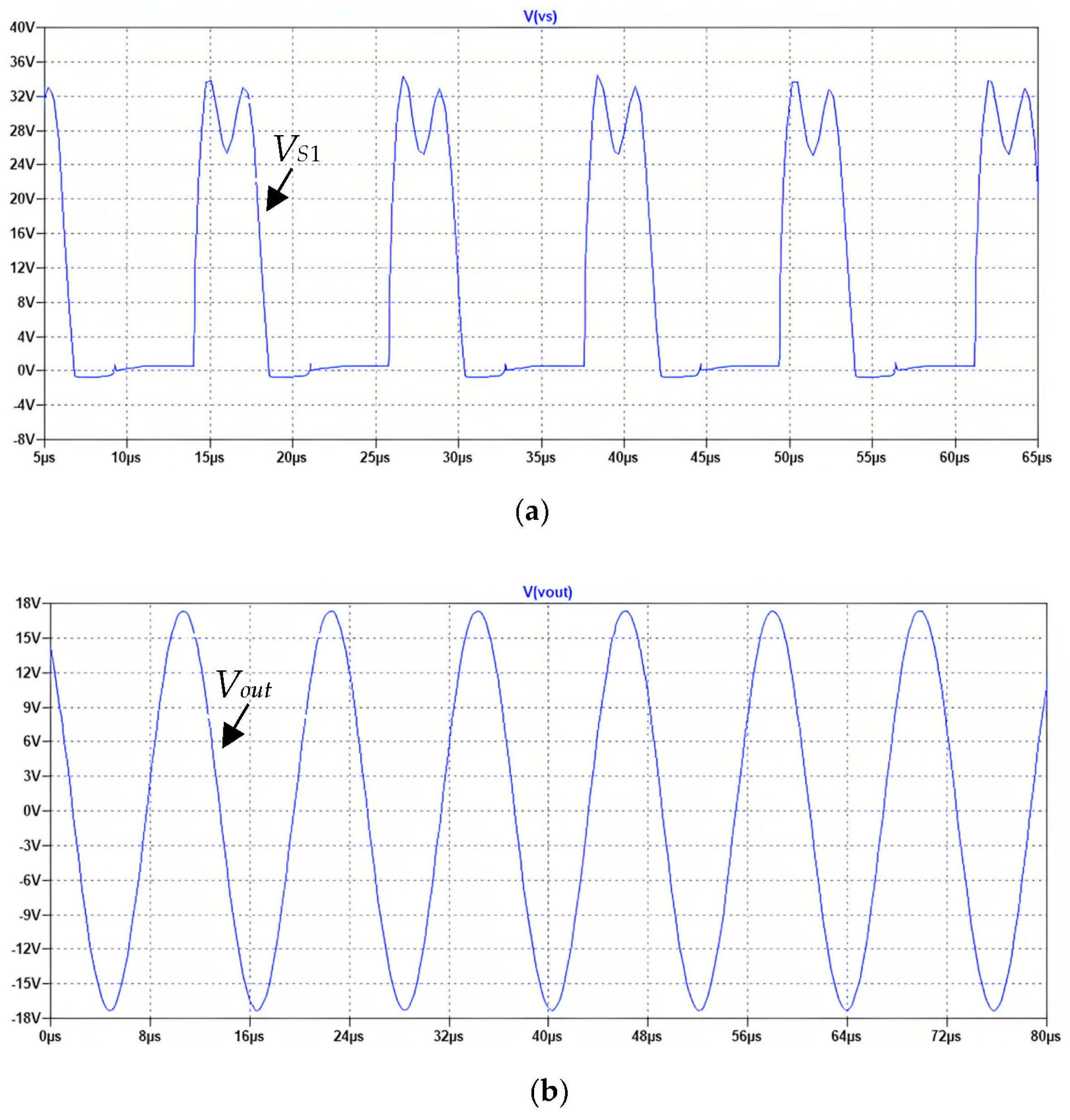
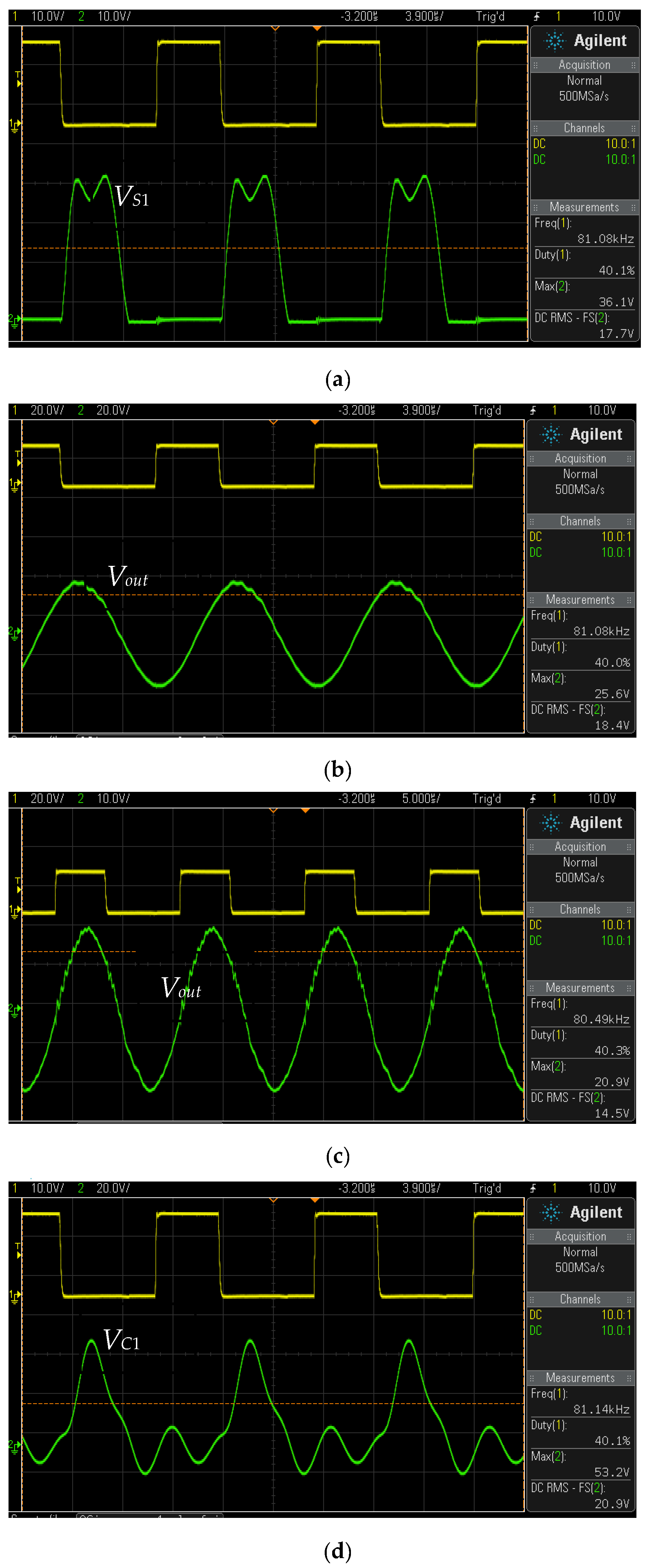
| Parameter | Simulation | Experimental |
|---|---|---|
| PT as primary resonant tank | ||
| Vout | 18 V | 20.9 V |
| VS1,peak | 34 V | 36.1 V |
| VC1,peak | 48 V | 53.2 V |
| PT as auxiliary resonant tank | ||
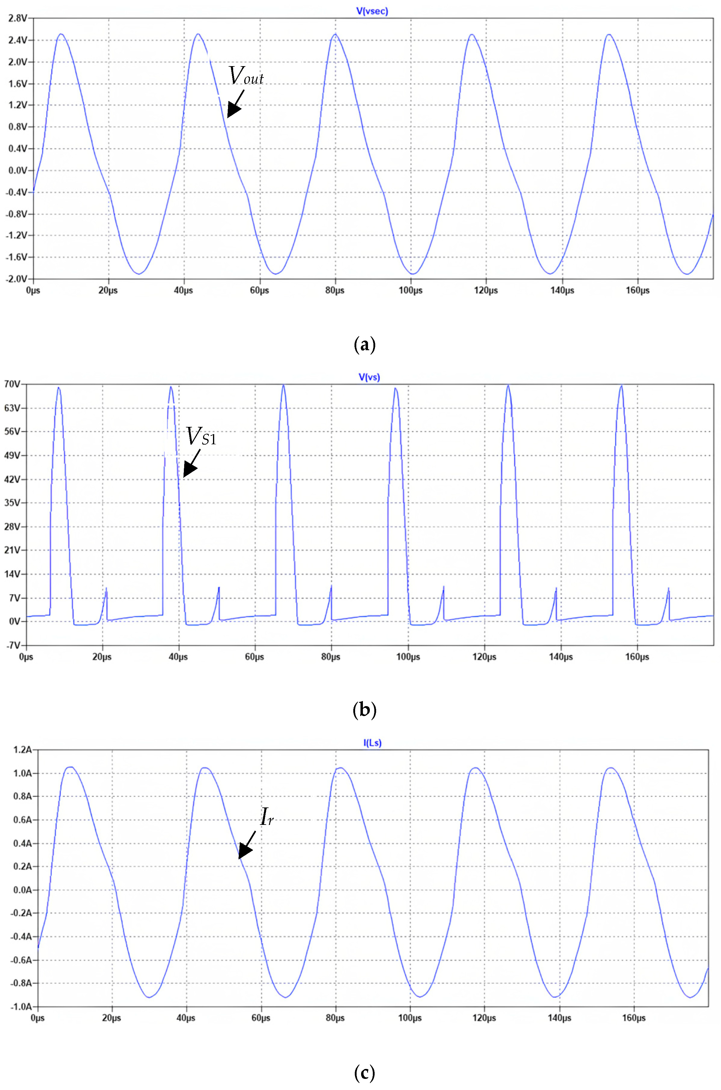
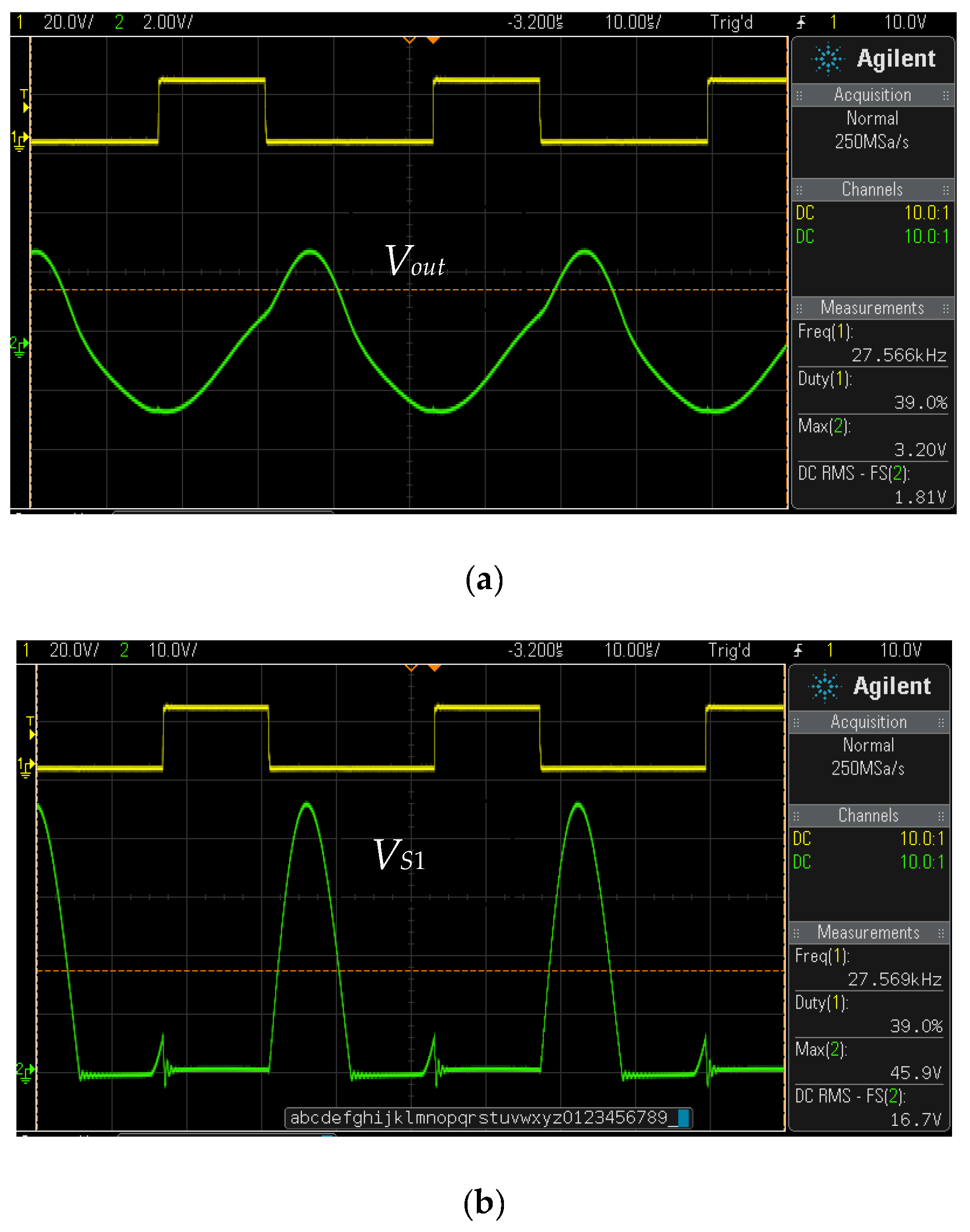
| Vout | 2.6 V | 3.2 V |
| VS1,peak | 70 V | 45.9 V |
Disclaimer/Publisher’s Note: The statements, opinions and data contained in all publications are solely those of the individual author(s) and contributor(s) and not of MDPI and/or the editor(s). MDPI and/or the editor(s) disclaim responsibility for any injury to people or property resulting from any ideas, methods, instructions or products referred to in the content. |
© 2023 by the authors. Licensee MDPI, Basel, Switzerland. This article is an open access article distributed under the terms and conditions of the Creative Commons Attribution (CC BY) license (https://creativecommons.org/licenses/by/4.0/).
Share and Cite
Ashique, R.H.; Arif, M.S.B.; Bhatti, A.R.; Al Mansur, A.; Maruf, M.H.; Shihavuddin, A. The ZVS Class E/F3 Inverter Using Piezoelectric Transformers for Energy Extraction. Electronics 2023, 12, 2118. https://doi.org/10.3390/electronics12092118
Ashique RH, Arif MSB, Bhatti AR, Al Mansur A, Maruf MH, Shihavuddin A. The ZVS Class E/F3 Inverter Using Piezoelectric Transformers for Energy Extraction. Electronics. 2023; 12(9):2118. https://doi.org/10.3390/electronics12092118
Chicago/Turabian StyleAshique, Ratil H., M. Saad Bin Arif, Abdul Rauf Bhatti, Ahmed Al Mansur, Md. Hasan Maruf, and ASM Shihavuddin. 2023. "The ZVS Class E/F3 Inverter Using Piezoelectric Transformers for Energy Extraction" Electronics 12, no. 9: 2118. https://doi.org/10.3390/electronics12092118
APA StyleAshique, R. H., Arif, M. S. B., Bhatti, A. R., Al Mansur, A., Maruf, M. H., & Shihavuddin, A. (2023). The ZVS Class E/F3 Inverter Using Piezoelectric Transformers for Energy Extraction. Electronics, 12(9), 2118. https://doi.org/10.3390/electronics12092118