Review

On-Chip Bus Protection against Soft Errors

1
Institute of Computer Engineering and Applied Informatics, Slovak University of Technology in Bratislava, 812 43 Bratislava, Slovakia
2
Institute of Informatics, Information Systems and Software Engineering, Slovak University of Technology in Bratislava, 812 43 Bratislava, Slovakia
*
Author to whom correspondence should be addressed.
Electronics 2023, 12(22), 4706; https://doi.org/10.3390/electronics12224706
Submission received: 16 October 2023 / Revised: 14 November 2023 / Accepted: 17 November 2023 / Published: 19 November 2023
(This article belongs to the Special Issue Progress and Future Development of Real-Time Systems on Chip)

Abstract

:
The increasing performance demands for processors leveraged in mission and safety-critical applications mean that the processors are implemented in smaller fabrication technologies, allowing a denser integration and higher operational frequency. Besides that, these applications require a high dependability and robustness level. The properties that provide higher performance also lead to higher susceptibility to transient faults caused by radiation. Many approaches exist for protecting individual processor cores, but the protection of interconnect buses is studied less. This paper describes the importance of protecting on-chip bus interconnects and reviews existing protection approaches used in processors for mission and safety-critical processors. The protection approaches are sorted into three groups: information, temporal, and spatial redundancy. Because the final selection of the protection approach depends on the use case and performance, power, and area demands, the three groups are compared according to their fundamental properties. For better context, the review also contains information about existing solutions for protecting the internal logic of the cores and external memories. This review should serve as an entry point to the domain of protecting the on-chip bus interconnect and interface of the core.

1. Introduction

Mission-critical applications (e.g., space satellites/probes) or safety-critical applications (e.g., automotive) require nowadays more processing performance than ever before. The deep-space applications may also require low power consumption. To fulfill these demands, the processors are implemented in smaller fabrication technologies, allowing a denser integration and higher operational frequency, which increases performance. On the other hand, they can preserve the performance with lower power consumption. The mission-critical space applications need to deal with high-radiation environments. Although this is a smaller problem for automotive applications thanks to the atmosphere and magnetic field of Earth, the safety of passengers requires extra attention. Radiation is a source of random hardware failures, a concern in functional safety standards like ISO 26262 [1]. These applications must preserve (at least) the dependability and robustness level with the transition to smaller fabrication technologies.
Radiation can be defined as a set of particles, charged or not, that can interact with the electronic system through an exchange of energy. When such a particle hits the semiconductor, it creates a scattering track during its penetration into the material and produces secondary particles [2]. If this ionization track traverses or comes close to the depletion region, the electric field rapidly collects carriers, creating a current/voltage glitch at that node. In general, the farther away from the junction the event occurs, the smaller the charge that will be collected. The sensitivity of the device depends primarily on the node capacitance, the operating voltage, and the strength of feedback transistors; all these factors define the amount of charge, or critical charge, required to trigger a change in the data state [3]. Generally, the outcomes of particle hits are called single-event effects (SEE). More precisely, a single event transient (SET) is an event when the glitch occurs in combination logic. This can result in save of incorrect values in a downstream memory element. A single event upset (SEU) means that the glitch occurs inside the memory element and directly causes a flip of the saved value.
A comprehensive study of the sensitivity of different fabrication technologies to the SEE effects was made in [4]. The outcomes are that the critical charge required to cause SEU in the static random-access memory (SRAM) constantly decreases, mainly on the supply voltage and load capacitance scaling trends of affected transistors. To analyze susceptibility to SET, a chain of inverters is used. The study points out that the SET pulse of inverters monotonically decreases but with a large spread. However, the frequency of the circuits also must be considered. As the frequency of the circuit increases, the pulse with the same duration has a higher probability of being latched. Another important factor is the increasing number of transistors per chip, which increases the number of places where the charge can be collected.
This paper reviews the existing protection approaches against transient faults of on-chip bus interconnects. It focuses on embedded processors used in safety/mission-critical applications like the automotive or space sector. Unfortunately, the standard bus communication protocols typically do not provide dedicated signals that could be leveraged for protection against these faults. Due to this, it is interesting to summarize and analyze which protection approaches are used in state-of-the-art processors. The efficient protection of processor cores is an interesting and hot topic, and many protection approaches have been published. However, their primary focus is to protect the processor core(s). It is common that they either completely omit the bus protection or that it is reduced only for providing checksum for data wires. We identified and compared several properties of three existing bus protection approaches: information, temporal, and spatial redundancy. This review should serve as an entry point to the domain of bus protection.
The paper is organized as follows. Section 2 describes basic approaches for protecting individual cores. Section 3 describes the solutions for protecting memory, including state-of-the-art examples. Section 4 describes the importance of protecting on-chip buses and reviews and compares current protection approaches. Section 5 provides a summary of the paper, and Section 6 discusses future steps.

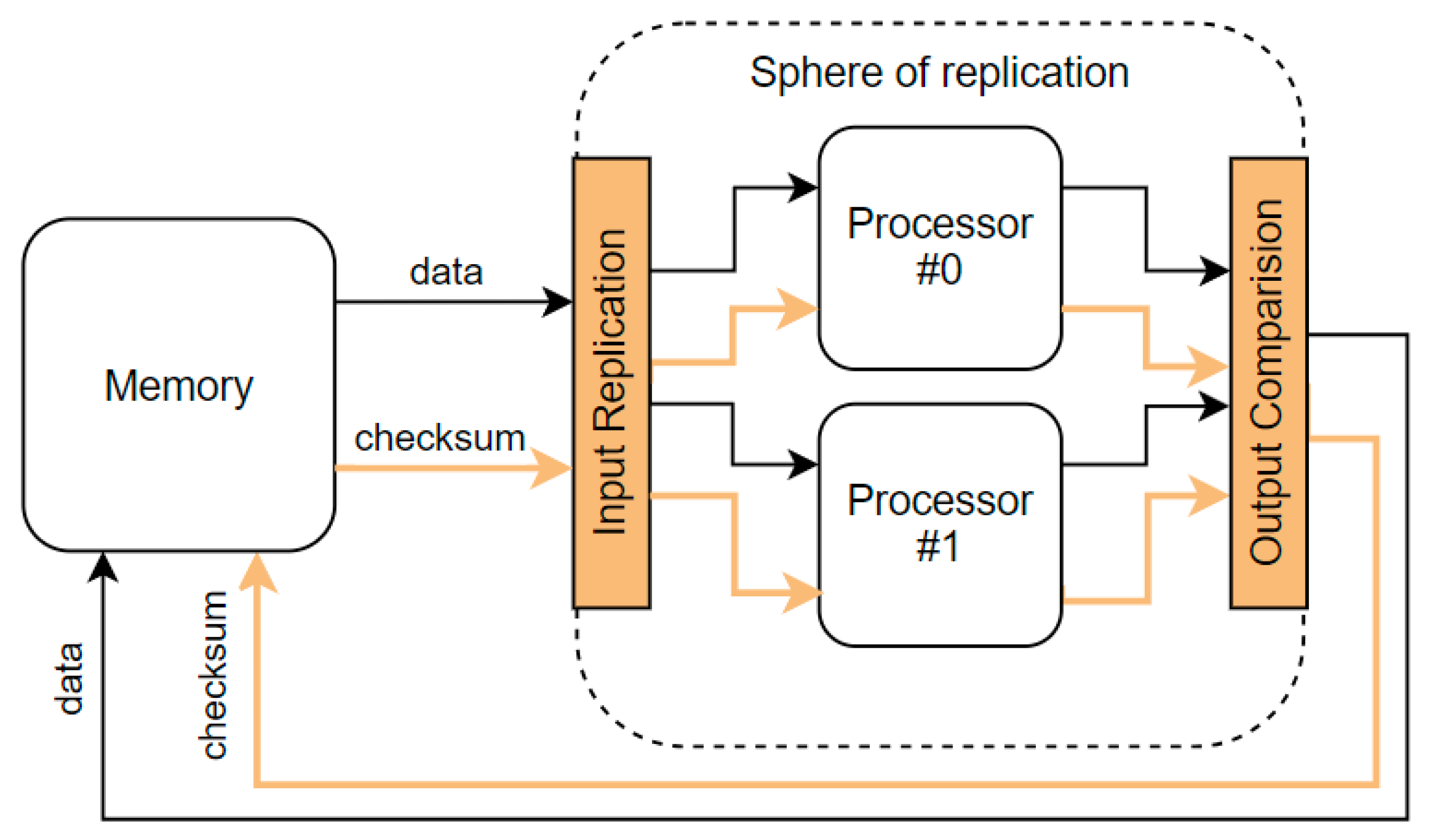
2. Protection of CPU Cores

The protection of the processor cores against soft errors could be realized at different design, manufacture, or usage levels. We have covered this topic in depth in [5]. Some processors use radiation hardened by process (RHBP) technologies [6,7], while others leverage commercial fabrication processes. The latter either leverage specialized technology libraries [8,9], lockstep execution [10,11,12], or redundant multithreading [13,14,15] or integrate the protection directly into the architecture of the pipeline [5,16,17,18]. These protection approaches are called radiation hardening by design (RHBD). Using a commercial fabrication process maximizes integration and performance capabilities and lowers cost, but the RHBD also offers a similar or higher tolerance to radiation effects than RHBP [19].

Sphere of Replication

The RHBD approaches are mostly based on hardware redundancy. Thus, we need to know the sphere of replication, which abstracts both the physical and logical redundancy of components. The components inside the sphere of replication enjoy fault coverage due to redundant execution. In contrast, components outside the sphere do not, so other techniques must cover them, such as information redundancy. All activity and state within the sphere are replicated in time or space. Values that cross the boundary of the sphere of replication are the outputs and inputs that require comparison and replication, respectively [20]. Any fault that occurs within the sphere of replication and propagates to its boundary will be detected by the fault detection scheme corresponding to the sphere of replication. Any outputs leaving the sphere of replication must be protected and checked for mismatch and corresponding faults. Any inputs into the sphere of replication must be appropriately replicated and delivered to the correct points within the sphere [21]. Figure 1 shows the sphere of replication that includes redundant copies of a processor. The data coming from not replicated memory, accompanied by a checksum to enable error detection and correction, enters the sphere of replication. The data and checksum provided by redundant cores are compared for detecting mismatches. They leave the sphere of replication as a protected pair without replication.
Replication of the memories would lead to high costs. For example, systems on chip (SoC) have more than half of their silicon area devoted to the static random-access memory (SRAM) for various purposes [22]. This means that in most cases, the sphere of replication includes only the processing core, and the boundary is its interface to other cores, memories, and peripherals. The core must be able to check the correctness of the inputs and provide protection at the outputs.

3. Memory Protection

The processing cores receive instructions from memory and provide results back to the memory (or peripherals). Due to the limitations of available technologies, we often talk about memory subsystems. Typically, the subsystem does not contain only one memory unit but contains a complex memory hierarchy. It consists of multiple levels of memory with different speeds and sizes. The faster memories are more expensive per bit than the slower memories and, thus, are smaller. The main memory is often implemented from dynamic random-access memory (DRAM), while levels closer to the processor (caches) use SRAM. DRAM is less costly per bit than SRAM, although it is substantially slower. The slowest memory types are nonvolatile memories like flash or magnetic disks [23]. Using a hierarchy also means that there may be more than one copy of data or instructions at different levels at a given time. This is when a copy value is preserved in a cache while the original value is kept in the main memory [24]. Memory can be a very sensitive part of integrated circuits concerning radiation effects. They often exhibit a high density of memory units and are a priority when reducing SEU effects [25]. This section provides information about available memory protections. Although this paper focuses on bus protection approaches, it is important to understand how the data can be protected in memory after being transferred through the bus.

3.1. Information Redundancy

Mitigation strategies based on spatial redundancy (duplication or triplication) are usually not well suited for large arrays of memory cells because of the high area cost. Information redundancy is a less costly solution for the required area. For example, parity or error correction and detection codes (EDAC) combined with bit interleaving or data scrambling can be used. Algorithms behind these codes can detect and correct errors in data by adding some redundant data to the original data. When the original data are read, their consistency can be checked with the redundant data [25]. The original data combined with the redundant (checksum) are called code words. A limit to the number of errors a code can detect or correct is determined by its minimum Hamming distance. The Hamming distance refers to the number of distinct bits between two code words. Given a code word space, the minimum Hamming distance of the code is defined as the minimum Hamming distance between any two valid (fault-free) code words in the space [21]. The bit-interleaving technique prevents that when a single ion hit provokes several physically adjacent bit flips inside the memory bank; those close-by bits do not belong to the same code word [25]. Due to optimizations [26], data scrambling occurs as part of the normal design practice of random-access memories (RAM). An example of memory cell scrambling is shown in Figure 2. The disadvantage is that interleaving makes the memory design more complex and requires more area. An alternative is to use EDACs that can correct adjacent errors [24]. In main memory systems composed of multiple DRAM chips, the interleaving is often performed across multiple chips, with each bit in the DRAM being covered by a different checksum. Then, if an entire DRAM chip experiences a hard fail and stops functioning, the data in that DRAM can be recovered using the other DRAM chips and the checksum [21]. The studies [27,28] compare different EDAC schemes for memories regarding hardware overhead, time overhead, and error correction and detection capabilities. Similarly, the study [29] compares existing approaches for L1 data cache error protection concerning performance, L2 cache bandwidth, power consumption, and area.
Parity and EDAC are the most popular cache protection techniques due to their design simplicity. Parity protection is preferred for higher-level (closer to a core, e.g., level 1) caches, while lower-level caches (far away from the core, e.g., level 2 or main memory) are commonly protected by EDAC in processors [30]. Even DRAM manufacturers have begun to use on-die EDAC, which silently corrects single-bit errors entirely within the DRAM chip, to cope with random single-bit errors that are increasingly frequent in smaller process technologies [31]. Parity-based methods often provide only fault detection, and error recovery is performed by bringing the correct copy of data from the lower-level memory. If a new value is written to the memory, the parity bits or checksum for the corresponding code word must also be updated. Information redundancy can bring additional complications to the design of the core. To calculate or check the checksum for data, the core must know the value of all bytes the checksum protects. Therefore, if the core is supposed to change only a subset of bytes, it must perform additional read accesses for the remaining bytes to calculate the checksum of the final code word.
Although the EDAC codes can detect and correct a specified number of faults in a code word, there is a possibility that particular faulty data are not needed for a longer period. Eventually, these data may receive another fault, leading to uncorrectable or even undetectable errors. For this reason, microcontrollers often incorporate scrubbing and monitoring functions. For example, the Hercules [32] EDAC controller gives developers the flexibility to manage the level of responsiveness to single-bit memory errors. There is an option for logging single-bit errors and setting a threshold to trigger a system-level alert if a critical number of errors occur. Some processors [9,33] integrate scrubbing of the memory blocks protected by EDAC to prevent fault accumulation. A GR740 SoC [33] includes a hardware memory scrubber peripheral. It can be programmed to scrub a memory area by reading through the memory and writing back the contents using a locked read-write cycle whenever a correctable error is detected. If an uncorrectable error is detected, that location is left untouched. The memory scrubber keeps track of the number of correctable errors and can be set up to interrupt when the counters exceed given thresholds. The EDAC-protected L2 cache of GR740 contains an additional internal scrubber to prevent the build-up of errors in the cache memories. Even the memories themselves can contain built-in self-repair mechanisms [34].
As discussed above, the core does not need to be responsible for correcting memory errors since other SoC components can be programmed to do that. On the other hand, the core should have access to information that errors were detected. If this is the case, a monitoring approach presented in [35] can be leveraged. The solution involves implementing an error handler component in the processor core that requests exception traps when detecting errors. Besides monitoring the internal structures of the core, the error handler also includes an external error input. The purpose of this signal is to enable the SoC to report errors in its structures, such as interconnections and peripherals. The study proposes the SoC error handler, which signals exceptions to the external error input of the error handler in the core. The SoC error handler gathers information about correctable and uncorrectable errors from the SDRAM EDAC controller and about bus access timeout events from the bus master controller.

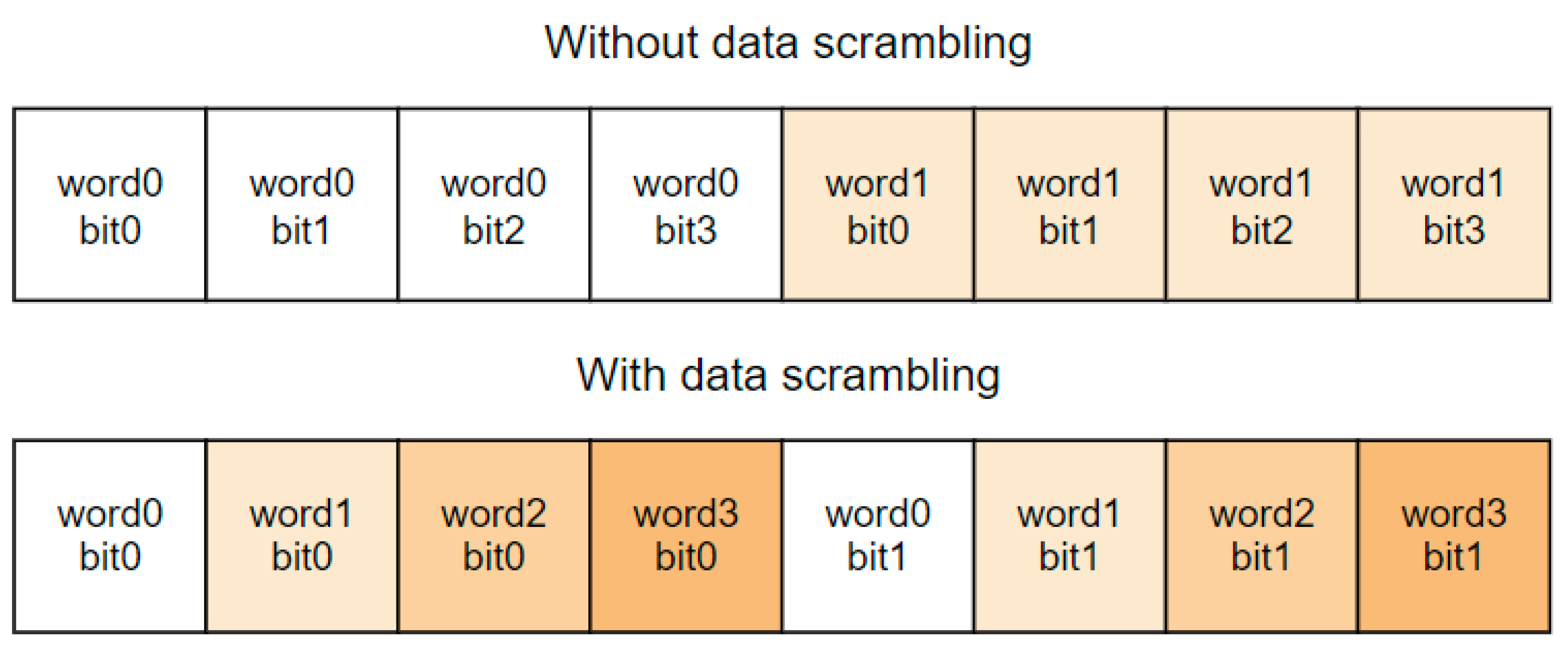
3.2. Hardening of Individual Memory Cells

Some techniques pursue hardening the individual bit storage cells by several means. They add resistors or capacitances on the feedback loop of the cell to increase its critical charge and, thus, increase its bit-flip threshold. Another solution is specific transistor sizing. Consequently, these cells do not scale easily as the device size is shrinking. The area cost of these cells can also be high. They can also increase the number of cell nodes, thus allowing for easier scaling. The cells are usually based on redundant storage of the information and feedback paths to restore the correct data [25]. An example of a hardened memory cell is the dual interlocked storage cell (DICE), which embeds 12 transistors in a memory cell structure [36]. Several emerging nonvolatile technologies are under development by major commercial foundries. They include a spin-transfer torque magnetic random-access memory (STT-MRAM), resistive random-access memory (ReRAM), phase change random-access memory (PCRAM), and conductive bridge random-access memory (CBRAM). These memories are relatively insensitive to ionizing radiation, SEEs, and displacement damage as there is no direct mechanism for interaction between radiation and the storage mechanism. When radiation-induced errors occur, it is most often a result of interaction with the select device or supporting complementary metal-oxide semiconductor (CMOS) peripheral circuitry [37].

3.3. State-of-the-Art of Memory Protection
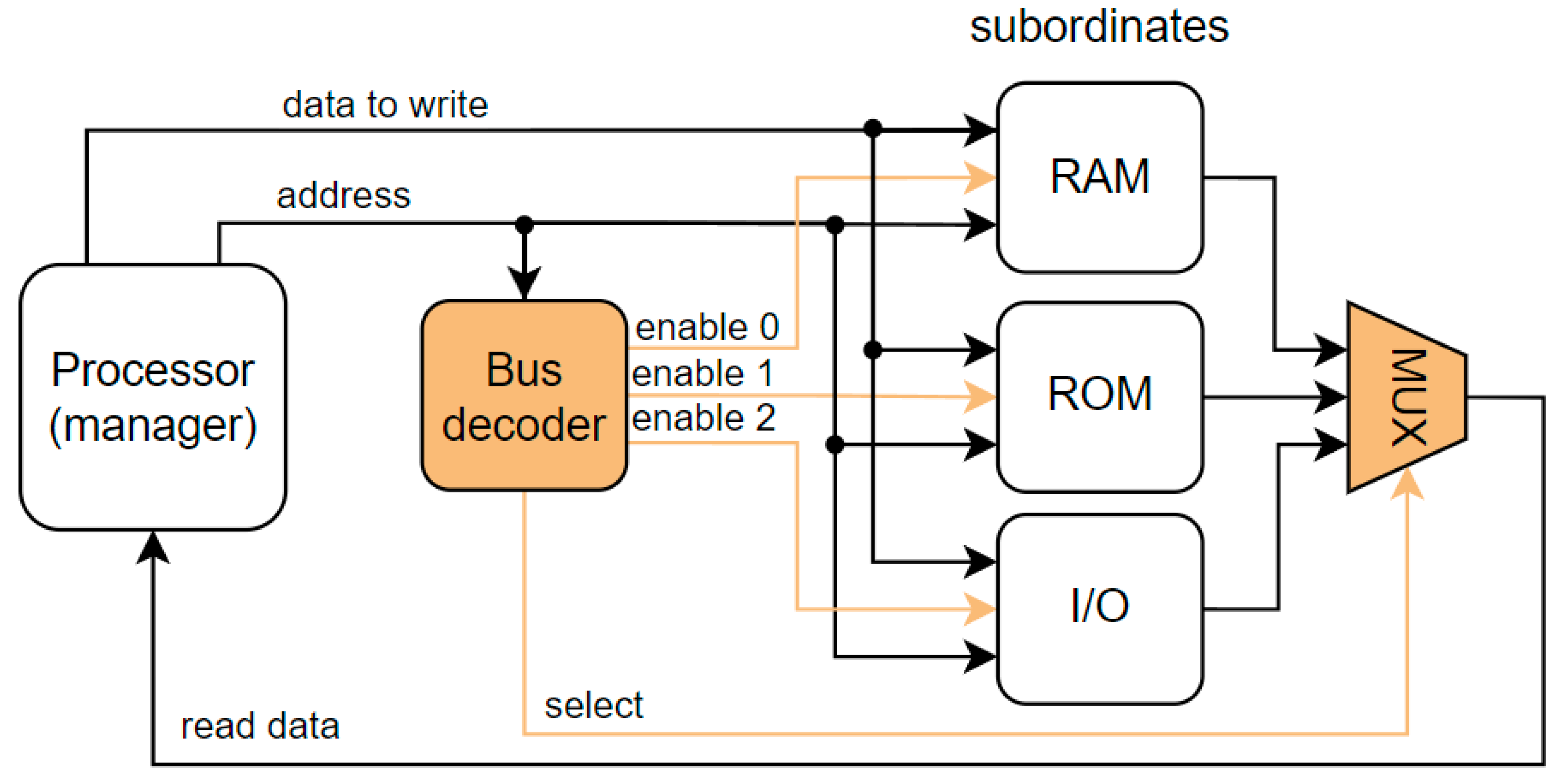
The L1 system of the Cortex-R5 [38] processor can contain access to caches (instruction and data) and tightly coupled memory (TCM). Both can be configured to detect and correct errors in their RAM. When the processor reads data from the RAMs, it checks that the redundant data are consistent with the real data and can either signal an error or attempt to correct it. The redundant data can be either parity or EDAC with different granularity. The processor leverages a read-modify-write process if a write of fewer bytes is required than the EDAC protects. For example, such a situation happens when the EDAC protects 32 bits, but the core should update only 16 bits. To compute the checksum for such a write, the processor must first read the 32-bit data from the RAM, then merge the data to be written with it to compute the checksum, and then write the data to the RAM, along with the new checksum. When a correctable error is detected in data read from the RAM, the processor has various ways of generating the correct data that follow two schemes. In the correct-inline scheme, the checksum bits are only used to correct the data read from the RAM, and these data are used. In the correct-and-retry scheme, the checksum is used to correct the data, which are then written back to the RAM. The processor then repeats the read access by re-executing the instruction that caused the read and reads the corrected data from the RAM if no more errors have occurred. This takes more clock cycles, at least nine, in the event of an error. It also increases the number of memory accesses required to execute the program, leads to higher power consumption, and can also lead to a decrease in performance. The behavior after detection of errors is more complex and depends on configuration—refer to the [38] for more information. Similar EDAC protection is also used for the Cortex-R4 [39] processors.
The AT697F [16] provides a direct memory interface to programmable read-only memory (PROM), memory-mapped I/O, asynchronous static RAM (SRAM), and synchronous dynamic RAM (SDRAM) devices. A protection with single error correction double error detection (SECDED) EDAC is available on each interface except I/O. A single-bit error qualifies as a correctable error. The correction is performed on the fly inside the processor during the current access, and no timing penalty is incurred. The correctable error event is reported in the registers, and an interrupt is generated if enabled. An uncorrectable error results in an exception. The processor can be configured to have an 8-bit SRAM. In this case, 32-bit load/store instructions are always performed as a sequence of 4 consecutive memory accesses. If EDAC protection is activated, a 5th byte read access is also performed to retrieve the checksum. The processor will always perform a full-word read-modify-write transaction on any sub-word store operation. The processor also contains cache memories protected using two parity bits per tag and per 4-byte data sub-block.
The GR740 SoC [33] contains an SDRAM memory controller with EDAC support. When writing, the controller generates the check bits and stores them along with the data. When reading, the controller will transparently correct any correctable errors and provide the corrected data on the bus. An extra corrected error output signal is asserted when a correctable read error occurs at the same cycle as the corrected data are delivered. This signal is connected to the memory scrubber. In case of an uncorrectable error, this is signaled by giving a bus error response. Only writes of 64-bit width or higher will translate directly into write cycles to the external memory. Other types of write accesses will generate a read-modify-write (RMW) cycle to update the checksum correctly. The SoC also contains memory control for the PROM/IO interface where the PROM area can be protected with SECDED EDAC. The behavior is similar to the previously mentioned controller, although some differences exist. Refer to the [33] for more information.

4. Bus Protection

It is not uncommon in an SoC for the AXI bus matrix to constitute around 20–30% of the die area, which, with increasing bus matrix sizes, means that a significant amount of logic is susceptible to soft errors [40]. Unfortunately, the standard protocols typically do not provide dedicated signals for protection against transient faults. So, it is up to the designers of the processor cores or SoC to integrate the protection. Otherwise, having protected memory would be worth nothing if the transfers between the memory and processing core were susceptible to faults. It was examined that transient faults on the bus matrix could have severe consequences, possibly leading to deadlock, memory corruption, or undefined behavior [40,41]. A simulation study [42] observed the highest rate of erroneous application outcomes due to soft errors in the crossbar interconnect (only components external to the core underwent fault injection). This section provides a review of proposed and currently used bus protection approaches.
The study described in [43] mentions that interconnect signal wires are at low risk of radiation-induced errors because currents resulting from radiation impact events are only induced in active regions and, thus, will only impart charge to the signal wires via an impact at the transmitter. In contrast, the large RC of the wire limits its effect at the receiver. However, it also notes that the receiver storage element nodes may be susceptible, particularly during the evaluation clock edge, when receiver designs target a minimal area. If the signal should run at high speed with appropriate integrity, it is often required to add buffers during physical synthesis. Such a buffer is a gate, typically two serially connected inverters, which regenerates a signal without changing functionality. In modern high-performance designs, buffers can comprise 10–20% of all standard cell instances [44]. Each buffer creates an active region. A particle strike on a regenerator buffer may result in a significant voltage glitch [45]. Such an event can result in sampling a faulty value from the affected signal. Existing approaches [45] for protecting these buffers come with disadvantages like increased area, power consumption, or constrained immunity.
The level-1 cache is typically part of the core, so the interface is proprietary. The communication with the remaining memory subsystem or peripherals is accomplished across industry-standard interfaces that sacrifice some performance for compatibility across multiple vendors [46]. Some of the popular standards include ARM Microcontroller Bus Architecture (AMBA) with several versions and specifications (e.g., AHB, AXI), IBM CoreConnect, STMicroelectronics STBus, Sonics SMART Interconnect, OpenCores Wishbone, and Altera Avalon [47]. In our research, we found that many automotive or space-grade processors leverage some version of the AMBA. It is widely used in various application-specific integrated circuits (ASIC) and SoC parts, including application processors in the Internet of Things (IoT) subsystems, smartphones, and networking SoCs [48]. Both specifications, AMBA AXI and AMBA AHB, share some properties, but the AXI is more complex and can also provide outstanding and out-of-order transactions. The exact description of protocols is outside the scope of this paper, but it is useful to provide a quick introduction. We chose AHB as it is simpler. A simplified block diagram is shown in Figure 3. The manager initiates the transfer. The decoder selects one of the subordinates (RAM, ROM, I/O) according to the address provided by the manager (processor). The selected subordinate receives requests and provides a response. The transfer consists of an address and a data phase. In the address phase, the request is delivered to the subordinate, and in the data phase, the data goes either from the manager to the subordinate or vice versa. The protocol has a pipelined nature, so both phases of the same transfer happen in different clock cycles. For detailed information about the AMBA protocols, refer to [48,49].
Integrating additional components to the SoC for direct monitoring of glitches in the bus may not be a safe solution. The particle hitting the regeneration buffer can affect only the output of the buffer, so the component would need to monitor the wire after the last buffer and before the intended destination component (subordinate, manager, or decoder). This can be a problem since the position of buffers is not known until synthesis. Due to this reason, the protection should ensure that the destination component will either tolerate faults or be able to detect and signal those events.

4.1. Existing Protection Approaches

For older technologies, the transient pulse generated by radiation-induced charge was quickly attenuated due to a large load capacitance and large propagation delays [25]. The combination of the low clock frequency of processors and the high critical charge leads to a low probability that a transient pulse is latched in the downstream latch. This means that processors implemented in those technologies focused mainly on protecting the memory elements. On the other hand, the newer state-of-the-art processors running at higher frequencies and implemented in the latest fabrication technologies, with lower critical charge, tend to protect the bus interconnect.
A wide range of protection approaches is primarily focused on providing protection for the processor core; we covered them in [5]. However, it is common that these approaches usually focus only on protecting the logic inside the sphere of replication while mentioning that the protection of the bus is outside the scope of the paper. Sometimes, the bus protection is reduced only to providing data EDAC checksum, or the protection is completely omitted. For example, it is assumed in [50] that the EDAC mechanism protects instruction and data memory, whereas the core in [18] provides only a checksum for data. Study [51] implements a soft-core processor into a field-programmable gate array (FPGA) while connecting a dedicated EDAC module between the core and memory, providing data encoding/decoding. The bus between memory and the multithreaded processor in a study detailed in [14] is EDAC-protected, but the study does not provide additional information. On the other hand, studies [52,53] do not mention protecting the external bus/memory. Our protection scheme presented in [5] also does not provide protection for the bus/memories. However, we have provided a guide on how the EDAC can be integrated with minimal impact on maximal frequency.
Arguably, most of the bus-based topologies leverage EDAC protection. The study [24] notes that using the same EDAC in the memory and for data movement is not recommended. Despite the simplicity, the achievable performance may not be optimal due to several factors. The different widths of the data bus and memory array can require different code rates, while the different types of errors that can occur during storage and transmission can be faced efficiently by different types of codes. As an example, interleaving is widely used in memories to prevent multiple adjacent upset of bits, but when a code word is fetched from the memory, it is no longer protected against this type of error. The data integrity of on-chip interconnection can be enhanced working at the layout level, for example, using suitable space rules, shielding, etc., or at the electrical level, using signal repeaters, low noise buffers, etc. Unfortunately, these solutions are strictly technology-dependent and are very sensitive to the technology shrink [24].

4.1.1. Information Redundancy

The study [54] analyzes the energy–reliability trade-off of using different protection approaches for on-chip communication in SoC using a 0.25 µm synthesis library and Leon processor. The on-chip interconnect was modeled as a noisy channel, and the focus was on reducing the power consumption while introducing additional information redundancy. The authors showed that the EDAC could, among enhancing reliability, reduce energy-per-bit dissipation. The reduced voltage swings counterbalance the energy overhead introduced by redundant signals. Although the study was not focused on soft errors, it provided an interesting outcome that retransmission (after fault detection) turns out to be more efficient than correction from the energy viewpoint. This is because the error-correcting decoder introduces a larger overhead (propagation delay and power consumption) for each transfer. In comparison, an error-detecting decoder incurs a smaller overhead at each transfer and an additional overhead (due to retransmission) of a few cycles only for corrupted transfers. The analysis was performed on the AMBA bus present between the cache and memory controller. The retransmission capability was integrated into the bus while preserving compliance with the AMBA protocol.
The protection of the AMBA 3 AXI bus with three different approaches for each set of signals is proposed in [40]. The control signals are protected with parity bits. The authors wanted to avoid a high drop in frequency due to the protection of the entire 32-bit address with inline parity, so they proposed to protect only a portion of the address bits by the parity. The constraint is that any fault in the unprotected bits should result in a transfer to the unmapped region, resulting in the AXI error response. It means that a special rearrangement of the memory map is required, reducing available memory address space. The data signals are protected with EDAC such that the checksum is sent on sideband signals in a clock cycle after the data. If the checksum does not correspond to the previous data, the entry is corrected according to the checksum. When an error is detected, the master is stalled by one cycle (if another transfer is requested) to allow for correction so that latency is only introduced when there is an error.
The L2 interface of the Cortex-R5 [38] processor can contain AXI and AHB interfaces for accessing memory and peripherals. These interfaces can be configured with bus EDAC to protect the integrity of individual signals. If enabled, the control and address signals are protected with parity. Each parity bit protects a maximum of eight bits. EDAC with SECDED capability is used to protect read and write data payload. Bus EDAC functionality checks for errors on every bus transfer the processor performs. This can include speculative accesses for which data are later discarded. The processor reports bus faults for all transfers whose data it uses and never reports bus data faults for transfers where the bus master sees an error response. The Cortex-R4 [39] may also support bus protection. If configured, the AXI master and slave channels are protected with parity bits.
The AURIX [55] family of microcontrollers, integrating TriCore processors, contain the shared resource interconnection (SRI) high-speed system bus. Each transaction consists of an address and data phase. The address phase is protected by an 8-bit EDAC checksum, covering all address phase signals except for request and grant. The data phase is protected by the 8-bit EDAC checksum, which covers the read/write data and most of the related address bits. Both EDACs have Hamming distance 4. The EDAC is only used for error detection.

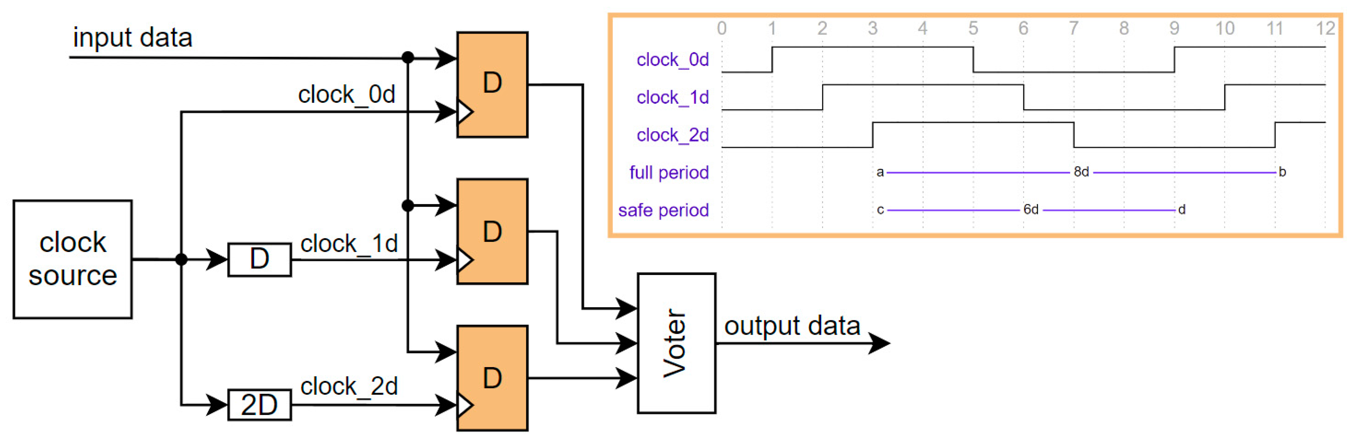
4.1.2. Temporal Redundancy

Although the AT697F [16] is fabricated in older 180 nm CMOS technology, and its maximal frequency is 100 MHz, it also protects against SET. The SoC implements a temporal sampling technique proposed in [56]. Each on-chip register is implemented using triple modular redundancy (TMR). The input data of each register making up one TMR module are sampled at different times, with the periods between sampling times exceeding the duration of a SET. The TMR connection of three registers with different input delays (0D, 1D, 2D) ensures that if the SET does not last more than D, a correct value is at the output. So, the SET is filtered out from the bus if it does not last more than D. A block diagram with waveforms is shown in Figure 4. The downside of this approach is that it reduces the maximal operational frequency due to integrated delays. The safe operation is guaranteed only if each register within the TMR sees the same clock period. For example, the clock skew in AT697F is optional and programmable, but if the maximum D is used, the clock frequency is decreased by 16.7%. This means the clock period is extended by two ns, protecting against transient glitches lasting less than one ns.
A natural temporal diversity is also present in redundant multithreading, where the redundant threads use the same bus but in distinct clock cycles. The redundant multithreading can be performed in hardware as in [13,14,15] or in software. The threads in the hardware solution execute the same binary, so it must be ensured that the trailing thread does not leverage already cached data requested by the leading thread. The software solutions use different memory regions for each thread, so the caching is not a problem.
Other types of SET filtering are presented in [57,58]. We are not aware that such type of filter has been used to protect bus signals in any processor yet. The filter uses an inverter string to delay the signal along one path and a guard gate to pass only those transients with widths exceeding the delay. A trade-off between performance and hardening is unavoidable. The wider the filtered SET pulse, the lower the maximum frequency of the design. The downside is that this penalty will become more severe with advancing technologies and lower operation of core voltages [57].

4.1.3. Spatial Redundancy

Some cores leverage replication of the interface. For example, the bus interface of the Hermes [17] core lies in the TMR region, allowing for a fully hard interface that can be voted at the periphery. Another simple protection by triplication of the interconnect and peripherals was performed in [59]. Replication of memories is also seen in multithreaded cores [13]. Although such protection is straightforward, it significantly increases area/routing and requires replicated memories/peripherals or additional voters before their inputs. The Dara [60] processor does not protect on-chip caches and off-chip memories. It is assumed that the I/O ports are far less vulnerable to soft errors than the in-chip units because they are driven by higher voltage. However, it is also mentioned that the I/O buses can easily apply EDAC or TMR to improve dependability. A processor protected with dual-core lockstep was presented in [11]. The cores leverage mechanisms of verification points, while each has its own data block RAM (BRAM) memory. Both cores have access to the same DDR memory, but it is unclear whether some protection exists.

4.2. Summary

Available bus protection approaches are based on one (or a combination) of the following principles: information redundancy, spatial redundancy, and temporal redundancy. Each protection approach has pros and cons. We have summarized these properties in detail in the following paragraphs and in Table 1, where colorized property means an advantage of a particular protection approach over the remaining approaches.
The parity and EDAC combination seems the most viable in the information redundancy group: the parity for address and control wires and the EDAC for the protection of data wires. Since the information redundancy constrains how many errors can be detected, it is important to lower the probability that a single particle hit produces transient faults in several wires protected by the same checksum. This requirement should be solvable during physical synthesis by adjusting the proximity or regeneration buffer of individual wires. The placement of encoders/decoders plays a critical role in affecting the operating frequency. For example, an encoder can generate the checksum in the same cycle as the data are being transferred (increasing register-to-output path) or a cycle before the transfer (increasing register-to-register path). It has been measured that the encoder for 32-bit data of SECDED code incurs 0.5 ns and the decoder 1.1 ns latency in a 90 nm standard cell ASIC library [61], whereas in the 250 nm library, the encoder incurs 2.31 ns and decoder 4.85 ns [54]. The SoCs for embedded systems often do not require full memory space, so reducing the timing penalty introduced for parity generation is possible by computing the parity bits only for the required number of address bits. The use of parity for protecting control wires should be fine-tuned, too. Some cores/interfaces may only require some of the signals the bus communication protocol provides. The fetch interface requires only reading from the memory and, most probably, does not require access to sub-word addresses and does not require the use of exclusive transfers. This simplifies the parity computation. It can also be worth providing look-up tables for the parity of control signals since the interfaces often leverage only a subset of available combinations of signal values. The subordinate unit should deny the transfer if the parity bits do not fit and respond with some error signaling. The response mainly comprises data but can contain a few wires for signaling errors or readiness. The parity generation should be easy and enough for those signals. If the manager observes a mismatch, the transfer can be repeated. The pipelining nature of communication protocols makes it hard (due to timing) to check, correct, and potentially deny incoming data if they contain an error. We recommend protecting the bus data wires with EDAC and saving the checksum with the data without checking their correctness during the transfer. In the case of memory, the data will be read together with the checksum, and the manager can eventually correct the data before using them. The system should contain some memory scrubber so the fault accumulation will not lead to undetected errors. Both memories and peripherals can also check the integrity of the data after completing the transfer. If an error is detected, they can use some signaling (e.g., interrupt), so the scrubber or processor core can react and potentially correct the data. Another important decision is to select how many bits the EDAC should protect. If the processor can write to fewer bits than the checksum protects, the core needs to read the content of the memory and merge it with the new data so the checksum of the code word can be generated. This means that for a single transaction, several data transfers are required. Although this has a big performance impact, the core can integrate a module with a write buffer to provide this operation without stalling the pipeline. Similar buffers are already used in the caches, so they can be modified instead of introducing new ones. The bus protocols may also define interconnect modules that help decode the transfer address and distribute requests to final subordinates. The protection of these modules is important, too. The most important requirement is to guarantee that the request will be delivered to the correct subordinate.
The usage of SET filtering represents temporal redundancy. It is a convenient type of protection since it does not require any changes at the interface of the core. Another benefit of the filters over the information redundancy is that it does not constrain the maximum wires with a faulty value. But it comes with a limitation. The filter must be set to the maximum duration of voltage glitch that can be tolerated. The wider the glitch the filter tolerates, the lower the maximum frequency of the bus can be. This solution also requires that the subordinates will either protect the saved data or the manager will provide some EDAC checksum for the data. An important note is that although the used filter will significantly constrain the maximum frequency of the bus, it does not mean that the frequency of the core will be constrained, too. Most modern processors used in SoC integrate L1 cache into the core while both running at the same frequency. The next-level caches or main memory can be significantly slower and run at lower frequencies. This means that introducing SET filters to the interface of the core does not have to result in significant performance degradation.
The replication of the interface is a typical representation of spatial redundancy. It is a straightforward protection approach, but it comes with many disadvantages. It increases area and power consumption by more than 200% and can impact timing. Another important question is whether the subordinates will be replicated or the subordinate side will vote on signals from individual interface replicas. The former option can be viable for memories but impossible for other peripherals. The latter option will require additional protection on the subordinate side so the data, in the case of memory, remain protected. On the other hand, if the memory is protected by replication, individual replicas may not need additional protection for preserving data. The processor core can compare incoming values and send the correct value to all replicas after the detected discrepancy.

5. Conclusions

To fulfill performance and power consumption requirements of mission/safety-critical demands, the processors are implemented in smaller fabrication technologies, allowing for a denser integration and higher operational frequency. Regardless of the size/count of transistors on the chip and its operating frequency, they must provide a high dependability and robustness level. Those performance-increasing properties lead to higher susceptibility to transient faults caused by radiation. Many approaches exist to protect individual processor cores, but they usually do not focus on the protection of the bus. This review paper focuses on existing bus protection approaches used in state-of-the-art processors and summarizes the proposed protection approaches. Individual approaches are sorted into information, temporal, and spatial redundancy groups. We have described the pros and cons and compared their properties. The comparison should serve as an entry point for a CPU architect to the domain of bus protection. The final selection of the protection depends on the use case of the processor, the operational environment, and the possibility of modifying components external to the processor. Information redundancy is viable for high-performance applications, but its implementation is not straightforward, so it should be reckoned at the beginning of the architecture design. The temporal redundancy may be added to the design in the advanced phases, but the duration of glitches constrains its protection. This means that it is suitable for low-performance applications and requires precise analysis of transient glitch durations for the target fabrication technology and operational environment. The spatial redundancy is the most straightforward, but it arguably has the biggest impact on chip area and power consumption. Replication of peripherals may be impossible, so voting of majority values would be necessary.

6. Future Directions

Our previous paper [5] proposed a novel redundancy-based protection scheme for the processor cores. It was integrated into the Hardisc RISC-V core with negligible impact on maximal frequency, whereas area and power consumption overheads were similar to the dual-core lockstep approaches. The Hardisc is available as an open-source project on GitHub; the link is provided in the Supplementary Materials. The proposed protection scheme has yet to integrate bus protection. We will leverage the review of available bus protection approaches present in this paper to protect the AMBA AHB bus interface of the Hardisc. We will protect it with information redundancy as we want to have as much protection integrated at the register transfer level as possible. Another reason is that the protection of fetch and data can be fine-tuned because they require distinct functionalities. The Hardisc also targets high operational frequency and low area and power overhead for protection, so the spatial and temporal approaches are not viable.

Supplementary Materials

The Hardisc repository: https://github.com/janomach/the-hardisc (accessed on 18 November 2023).

Author Contributions

Conceptualization, J.M.; methodology, J.M.; software, J.M.; validation, J.M.; formal analysis, J.M.; investigation, J.M.; resources, J.M.; data curation, J.M.; writing—original draft preparation, J.M.; writing—review and editing, J.M. and L.K.; visualization, J.M.; supervision, L.K. and P.Č.; project administration, L.K.; funding acquisition, L.K. and P.Č. All authors have read and agreed to the published version of the manuscript.

Funding

The work reported here was supported by the Operational Programme Integrated Infrastructure for the project Advancing University Capacity and Competence in Research, Development and Innovation (ACCORD) (ITMS code: 313021X329), co-funded by the European Regional Development Fund (ERDF). This publication was also supported in part by the Slovak national project KEGA 025STU-4/2022, APVV-19-0401, and APVV-20-0346.

Data Availability Statement

Not applicable.

Conflicts of Interest

The authors declare no conflict of interest.

References

  1. ISO 26262-1:2018(E); Road Vehicles—Function Safety. Second edition 2018–12. International Standard ISO: Geneva, Switzerland, 2018.
  2. Battezzati, N.; Sterpone, L.; Violante, M. Reconfigurable Field Programmable Gate Arrays for Mission-Critical Applications; Springer: New York, NY, USA, 2011. [Google Scholar] [CrossRef]
  3. Baumann, R. Soft Errors in Advanced Computer Systems. IEEE Des. Test Comput. 2005, 22, 258–266. [Google Scholar] [CrossRef]
  4. Kobayashi, D. Scaling Trends of Digital Single-Event Effects: A Survey of SEU and SET Parameters and Comparison With Transistor Performance. IEEE Trans. Nucl. Sci. 2021, 68, 124–148. [Google Scholar] [CrossRef]
  5. Mach, J.; Kohútka, L.; Čičák, P. In-Pipeline Processor Protection against Soft Errors. J. Low Power Electron. Appl. 2023, 13, 33. [Google Scholar] [CrossRef]
  6. Microchip Technology Inc. SAMRH71 Rad-Hard 32-bit Arm® Cortex®-M7, Microcontroller for Aerospace Applications, Complete Data Sheet, DS60001593H; Microchip Technology Inc.: Chandler, AZ, USA, 2022. [Google Scholar]
  7. Haddad, N.F.; Brown, R.D.; Ferguson, R.; Kelly, A.T.; Lawrence, R.K.; Pirkl, D.M.; Rodgers, J.C. Second generation (200 MHz) RAD750 microprocessor radiation, evaluation. In Proceedings of the 2011 12th European Conference on Radiation and Its Effects on Components and Systems, Seville, Spain, 19–23 September 2011; pp. 877–880. [Google Scholar] [CrossRef]
  8. Cobham Gaisler AB. GR740 Radiation Summary, Test Report, Doc. No. GR740-RADS-1-1-3, Issue 1.3. 2020. Available online: https://gaisler.com/doc/gr740/GR740-RADS-1-1-3_GR740_Radiation_Summary.pdf (accessed on 18 November 2023).
  9. CAES. Gaisler NOEL-V SoC Applications and Ecosystem, RISC-V in Space 2022. Available online: http://microelectronics.esa.int/riscv/rvws2022/presentations/06_ESA_RISC-V_in_Space-NOEL-V.pdf (accessed on 23 April 2023).
  10. Iturbe, X.; Venu, B.; Ozer, E.; Poupat, J.-L.; Gimenez, G.; Zurek, H.-U. The Arm Triple Core Lock-Step (TCLS) Processor. ACM Trans. Comput. Syst. 2018, 36, 7. [Google Scholar] [CrossRef]
  11. de Oliveira, A.B.; Rodrigues, G.S.; Kastensmidt, F.L.; Added, N.; Macchione, E.L.A.; Aguiar, V.A.P.; Medina, N.H.; Silveira, M.A.G. Lockstep Dual-Core ARM A9: Implementation and Resilience Analysis Under Heavy Ion-Induced Soft Errors. IEEE Trans. Nucl. Sci. 2018, 65, 1783–1790. [Google Scholar] [CrossRef]
  12. Marcinek, K.; Pleskacz, W.A. Variable Delayed Dual-Core Lockstep (VDCLS) Processor for Safety and Security Applications. Electronics 2023, 12, 464. [Google Scholar] [CrossRef]
  13. Sim, M.T.; Zhuang, Y. A Dual Lockstep Processor System-on-a-Chip for Fast Error Recovery in Safety-Critical Applications. In Proceedings of the IECON 2020 the 46th Annual Conference of the IEEE Industrial Electronics Society, Singapore, 18–21 October 2020; pp. 2231–2238. [Google Scholar]
  14. Barbirotta, M.; Cheikh, A.; Mastrandrea, A.; Menichelli, F.; Vigli, F.; Olivieri, M. A Fault Tolerant soft-core obtained from an Interleaved-Multi-Threading RISC-V microprocessor design. In Proceedings of the 2021 IEEE International Symposium on Defect and Fault Tolerance in VLSI and Nanotechnology Systems (DFT), Athens, Greece, 6–8 October 2021; pp. 1–4. [Google Scholar]
  15. Barbirotta, M.; Cheikh, A.; Mastrandrea, A.; Menichelli, F.; Ottavi, M.; Olivieri, M. Evaluation of Dynamic Triple Modular Redundancy in an Interleaved-Multi-Threading RISC-V Core. J. Low Power Electron. Appl. 2023, 13, 2. [Google Scholar] [CrossRef]
  16. Atmel Corporation. Rad-Hard 32 Bit SPARC V8 Processor AT697F, Rev. 7703E–AERO–08/11. 2011. Available online: https://ww1.microchip.com/downloads/en/DeviceDoc/doc7703.pdf (accessed on 23 April 2023).
  17. Clark, L.T.; Duvnjak, A.; Cannon, M.; Brunhaver, J.; Agarwal, S.; Manuel, J.E.; Wilson, D.; Barnaby, H.; Marinella, M. A Soft-Error Hardened by Design Microprocessor Implemented on Bulk 12-nm FinFET CMOS. IEEE Trans. Nucl. Sci. 2022, 69, 1602–1609. [Google Scholar] [CrossRef]
  18. Gupta, S.; Gala, N.; Madhusudan, G.S.; Kamakoti, V. SHAKTI-F: A Fault Tolerant Microprocessor Architecture. In Proceedings of the 2015 IEEE 24th Asian Test Symposium (ATS), Mumbai, India, 22–25 November 2015; pp. 163–168. [Google Scholar]
  19. Ginosar, R. Ramon Chips, Ltd. Survey of Processors for Space, DASIA. 2012. Available online: https://docs.wixstatic.com/ugd/418640_087c23c99df24aa8acbf01b96dcd281a.pdf?index=true (accessed on 23 April 2023).
  20. Reinhardt, K.S.; Mukherjee, S.S. Transient fault detection via simultaneous multithreading. In Proceedings of the 27th International Symposium on Computer Architecture (IEEE Cat. No.RS00201), Vancouver, BC, Canada, 10–14 June 2000; pp. 25–36. [Google Scholar]
  21. Mukherjee, S. Architecture Design for Soft Errors; Elsevier Inc.: Amsterdam, The Netherlands, 2008. [Google Scholar] [CrossRef]
  22. Greaves, D.J. System on Chip Design and Modelling. In University of Cambridge Computer Laboratory Lecture Notes; 2011; Available online: https://www.cl.cam.ac.uk/teaching/1011/SysOnChip/socdam-notes1011.pdf (accessed on 18 November 2023).
  23. Patterson, D.A.; Hennessy, J.L. Computer Organization and Design RISC-V Edition: The Hardware Software Interface, 1st. ed.; Morgan Kaufmann Publishers Inc.: San Francisco, CA, USA, 2017. [Google Scholar]
  24. Ottavi, M.; Gizopoulos, D.; Pontarelli, S. Dependable Multicore Architectures at Nanoscale; Springer International Publishing AG: Berlin/Heidelberg, Germany, 2018. [Google Scholar] [CrossRef]
  25. ECSS-Q-HB-60-02A; Techniques for Radiation Effects Mittigation in ASICs and FRGAs Hadbook. ECSS Secretariat ESA-ESTEC Requirements & Standards Division: Noordwijk, The Netherlands, 2016. Available online: http://microelectronics.esa.int/asic/ECSS-Q-HB-60-02A1September2016.pdf (accessed on 23 April 2023).
  26. van de Goor, A.; Schanstra, I. Address and data scrambling: Causes and impact on memory tests. In Proceedings of the First IEEE International Workshop on Electronic Design, Test and Applications 2002, Christchurch, New Zealand, 29–31 January 2002; pp. 128–136. [Google Scholar] [CrossRef]
  27. Chen, M.; Guo, C.; Chen, L.; Li, W.; Zhang, F.; Hu, X.; Xu, J. Research on EDAC Schemes for Memory in Space Applications. Electronics 2021, 10, 533. [Google Scholar] [CrossRef]
  28. Song, Y.; Park, S.; Sullivan, M.B.; Kim, J. SEC-BADAEC: An Efficient ECC with No Vacancy for Strong Memory Protection. IEEE Access 2022, 10, 89769–89780. [Google Scholar] [CrossRef]
  29. Sadler, N.N.; Sorin, D.J. Choosing an Error Protection Scheme for a Microprocessor’s L1 Data Cache. In Proceedings of the 2006 International Conference on Computer Design, San Jose, CA, USA, 1–4 October 2006; pp. 499–505. [Google Scholar] [CrossRef]
  30. Ko, Y.; Jeyapaul, R.; Kim, Y.; Lee, K.; Shrivastava, A. Protecting Caches from Soft Errors. ACM Trans. Embed. Comput. Syst. 2017, 16, 93. [Google Scholar] [CrossRef]
  31. Patel, M.; Kim, J.S.; Shahroodi, T.; Hassan, H.; Mutlu, O. Bit-Exact ECC Recovery (BEER): Determining DRAM On-Die ECC Functions by Exploiting DRAM Data Retention Characteristics. In Proceedings of the 2020 53rd Annual IEEE/ACM International Symposium on Microarchitecture (MICRO), Athens, Greece, 17–21 October 2020; pp. 282–297. [Google Scholar] [CrossRef]
  32. Greb, K.; Pradhan, D. Texas Instruments, Hercules™ Microcontrollers: Real-Time MCUs for Safety-Critical Products; Texas Instruments: Dallas, TX, USA, 2011; Available online: https://www.ti.com/lit/fs/spry178/spry178.pdf?ts=1700302644823&ref_url=https%253A%252F%252Fwww.google.com%252F (accessed on 18 November 2023).
  33. GR740, Quad Core LEON4 SPARC V8 Processor, Version 2.6; Frontgrade Gaisler AB: Goteborg, Sweden, 2023.
  34. Su, C.-L.; Yeh, Y.-T.; Wu, C.-W. An integrated ECC and redundancy repair scheme for memory reliability enhancement. In Proceedings of the 20th IEEE International Symposium on Defect and Fault Tolerance in VLSI Systems (DFT’05), Monterey, CA, USA, 3–5 October 2005; pp. 81–89. [Google Scholar] [CrossRef]
  35. Santos, D.A.; Mattos, A.M.P.; Melo, D.R.; Dilillo, L. Enhancing Fault Awareness and Reliability of a Fault-Tolerant RISC-V System-on-Chip. Electronics 2023, 12, 2557. [Google Scholar] [CrossRef]
  36. Calin, T.; Velazco, R.; Nicolaidis, M.; Moss, S.; LaLumondiere, S.; Tran, V.; Koga, R.; Clark, K. Topology-related upset mechanisms in design hardened storage cells. RADECS 97. In Proceedings of the Fourth European Conference on Radiation and Its Effects on Components and Systems (Cat. No.97TH8294), Cannes, France, 15–19 September 1997; pp. 484–488. [Google Scholar] [CrossRef]
  37. Marinella, M.J. Radiation Effects in Advanced and Emerging Nonvolatile Memories. IEEE Trans. Nucl. Sci. 2021, 68, 546–572. [Google Scholar] [CrossRef]
  38. Cortex™-R5 and Cortex-R5F, Technical Reference Manual, Revision: r1p1, ARM DDI 0460C (ID021511). 2011. Available online: https://documentation-service.arm.com/static/5f042788cafe527e86f5cc83?token= (accessed on 18 November 2023).
  39. Cortex™-R4 and Cortex-R4F, Technical Reference Manual, Revision: r1p4, ARM DDI 0363G (ID041111). 2011. Available online: https://documentation-service.arm.com/static/5f0358e8dbdee951c1cd6f3b?token= (accessed on 18 November 2023).
  40. Graham, D.; Strid, P.; Roy, S.; Rodriguez, F. A low-tech solution to avoid the severe impact of transient errors on the IP interconnect. In Proceedings of the 2009 IEEE/IFIP International Conference on Dependable Systems & Networks, Lisbon, Portugal, 29 June–2 July 2009; pp. 478–483. [Google Scholar] [CrossRef]
  41. Lin, I.-C.; Srinivasan, S.; Vijaykrishnan, N.; Dhanwada, N. Transaction Level Error Susceptibility Model for Bus Based SoC Architectures. In Proceedings of the 7th International Symposium on Quality Electronic Design (ISQED’06), San Jose, CA, USA, 27–29 March 2006; pp. 6–780. [Google Scholar] [CrossRef]
  42. Cho, H.; Cher, C.-Y.; Shepherd, T.; Mitra, S. Understanding soft errors in uncore components. In Proceedings of the 52nd Annual Design Automation Conference (DAC ‘15). Association for Computing Machinery, New York, NY, USA, 8–12 June 2015; pp. 1–6. [Google Scholar] [CrossRef]
  43. Postman, J.; Chiang, P. A Survey Addressing On-Chip Interconnect: Energy and Reliability Considerations. Int. Sch. Res. Not. 2012, 2012, 916259. [Google Scholar] [CrossRef]
  44. Kahng, A.B.; Lienig, J.; Markov, I.L.; Hu, J. VLSI Physical Design: From Graph Partitioning to Timing Closure, 1st ed.; Springer Publishing Company, Incorporated: Berlin/Heidelberg, Germany, 2011. [Google Scholar]
  45. Dash, R.; Garg, R.; Khatri, S.P.; Choi, G. SEU hardened clock regeneration circuits. In Proceedings of the 2009 10th International Symposium on Quality Electronic Design, San Jose, CA, USA, 16–18 March 2009; pp. 806–813. [Google Scholar] [CrossRef]
  46. Shen, J.P.; Lipasti, M.H. Moder Processor Design: Fundamentals of Superscalar Processors; Waveland Press, Inc.: Long Grove, IL, USA, 2013; ISBN 978-1-4786-0783-0. [Google Scholar]
  47. Pasricha, S.; Dutt, N. On-Chip Communication Architectures, 1st ed.; Elsevier: Amsterdam, The Netherlands, 2008; ISBN 978-0-12-373892-9. [Google Scholar]
  48. Introduction to AMBA AXI4, Issue 0101; ARM Limited: Cambridge, UK, 2020.
  49. IHI 0033C, AMBA® AHB Protocol Specification; ARM Limited: Cambridge, UK, 2021.
  50. Nikiema, P.R.; Kritikakou, A.; Traiola, M.; Sentieys, O. Design with low complexity fine-grained Dual Core Lock-Step (DCLS) RISC-V processors. In Proceedings of the 2023 53rd Annual IEEE/IFIP International Conference on Dependable Systems and Networks—Supplemental Volume (DSN-S), Porto, Portugal, 27–30 June 2023; pp. 224–229. [Google Scholar] [CrossRef]
  51. Rao, A.S.; Kudtarkar, A.; Harakuni, L.; Rao, G.N.; Sudeendra, K.K. A Generic On-Board Computer based on RISC-V Architecture Processor for Low Cost Nanosatellite Applications. In Proceedings of the 2023 2nd International Conference on Vision Towards Emerging Trends in Communication and Networking Technologies (ViTECoN), Vellore, India, 5–6 May 2023; pp. 1–6. [Google Scholar]
  52. Li, J.; Zhang, S.; Bao, C. DuckCore: A Fault-Tolerant Processor Core Architecture Based on the RISC-V ISA. Electronics 2022, 11, 122. [Google Scholar] [CrossRef]
  53. Silva, I.; do Espírito Santo, O.; do Nascimento, D.; Xavier-de-Souza, S. Cevero: A soft-error hardened soc for aerospace applications. In Anais Estendidos do X Simpósio Brasileiro de Engenharia de Sistemas Computacionais; SBC: Porto Alegre, Brasil, 2020; pp. 121–126. [Google Scholar]
  54. Bertozzi, D.; Benini, L.; De Micheli, G. Error control schemes for on-chip communication links: The energy-reliability tradeoff. IEEE Trans. Comput. -Aided Des. Integr. Circuits Syst. 2005, 24, 818–831. [Google Scholar] [CrossRef]
  55. Aurix Efficiency Platform TC21x/TC22x/TC23x User’s Manual, V1.1 2014-12; Infineon Technologies AG: Munich, Germany, 2014; Available online: https://community.infineon.com/gfawx74859/attachments/gfawx74859/AURIX/5399/1/Infineon-TC21x-TC22x-TC23x-UM-v01_01-EN.pdf (accessed on 18 November 2023).
  56. Mavis, D.; Eaton, P. Soft error rate mitigation techniques for modern microcircuits. 2002 IEEE International Reliability Physics Symposium Proceedings. In Proceedings of the 40th Annual (Cat. No.02CH37320), Dallas, TX, USA, 7–11 April 2002; pp. 216–225. [Google Scholar] [CrossRef]
  57. Rezgui, S.; Wang, J.J.; Tung, E.C.; Cronquist, B.; McCollum, J. New Methodologies for SET Characterization and Mitigation in Flash-Based FPGAs. IEEE Trans. Nucl. Sci. 2007, 54, 2512–2524. [Google Scholar] [CrossRef]
  58. Mitra, S.; Zhang, M.; Waqas, S.; Seifert, N.; Gill, B.; Kim, K.S. Combinational Logic Soft Error Correction. In Proceedings of the 2006 IEEE International Test Conference, Santa Clara, CA, USA, 22–27 October 2006; pp. 1–9. [Google Scholar] [CrossRef]
  59. Lázaro, J.; Astarloa, A.; Zuloaga, A.; Araujo, J.; Jiménez, J. AXI Lite Redundant On-Chip Bus Interconnect for High Reliability Systems. IEEE Trans. Reliab. 2023, 1–6. [Google Scholar] [CrossRef]
  60. Yao, J.; Okada, S.; Masuda, M.; Kobayashi, K.; Nakashima, Y. DARA: A Low-Cost Reliable Architecture Based on Unhardened Devices and Its Case Study of Radiation Stress Test. IEEE Trans. Nucl. Sci. 2012, 59, 2852–2858. [Google Scholar] [CrossRef]
  61. Naseer, R.; Draper, J. DEC ECC design to improve memory reliability in sub-100nm technologies. In Proceedings of the IEEE International Conference on Electronics, Circuits and Systems, St. Julien’s, Malta, 31 August–3 September 2008; pp. 586–589. [Google Scholar] [CrossRef]
Figure 1. Sphere of replication and protected memory.
Electronics 12 04706 g001
Figure 2. Example of data in memory with and without data scrambling.
Electronics 12 04706 g002
Figure 3. Simplified block diagram of a system with AMBA AHB bus.
Electronics 12 04706 g003
Figure 4. Temporal redundancy with delay (D) in the replicated clock signals.
Electronics 12 04706 g004
Table 1. Comparison of bus protection approaches.
Property/Characteristic Redundancy
InformationTemporalSpatial
Concurrent glitches in multiple wires can be undetected YesNoPartially
Protection is limited by the duration of the glitchNoYesNo
Impacts bus clock frequencyPartiallyYesPartially
Increases bus transfer latency (in clock cycles)PartiallyNoPartially
Increases area for the interconnectionPartiallyPartiallyYes
Requires changes to the managerYesNoPartially
Requires changes to the subordinatesYesNoNo
Implementation is straightforwardNoPartiallyYes
Usable for data protection of data in memoryYesNoYes
Some transactions may need several transfersYesNoNo
Fine-tunable for a specific interfaceYesNoNo
Used in state-of-the-art processorsYesYesPartially
Disclaimer/Publisher’s Note: The statements, opinions and data contained in all publications are solely those of the individual author(s) and contributor(s) and not of MDPI and/or the editor(s). MDPI and/or the editor(s) disclaim responsibility for any injury to people or property resulting from any ideas, methods, instructions or products referred to in the content.

