Article

A 10 GHz Compact Balun with Common Inductor on CMOS Process

1
College of Advanced Manufacturing Innovation, King Mongkut’s Institute of Technology Ladkrabang, Bangkok 10520, Thailand
2
Department of Electronic Engineering, National Taipei University of Technology, Taipei 10608, Taiwan
*
Author to whom correspondence should be addressed.
Electronics 2023, 12(2), 468; https://doi.org/10.3390/electronics12020468
Submission received: 17 December 2022 / Revised: 6 January 2023 / Accepted: 13 January 2023 / Published: 16 January 2023
(This article belongs to the Special Issue Microwave Subsystems and Wireless Propagation)

Abstract

:
This paper presents a compact balun with a common inductor design. The design used Wilkinson-type balun topology with modified lumped transmission lines and a common inductor to realize circuit size reduction on a lossy CMOS process. Measurements of the prototype chip had a reflection coefficient below 17.8 dB at all ports, an insertion loss of 1.98 dB, and an isolation of 16.8 dB. The chip size was only 0.025λ0 × 0.034λ0.

1. Introduction

Baluns have been used widely in many microwave and millimeter-wave applications such as antenna feed networks, balanced mixers, push–pull power amplifiers, and frequency doublers. For power requirement categorization, baluns can be divided into passive and active. Active baluns are usually unidirectional signal couplers. Their advantages are circuit gain and less chip area [1,2,3]. Nevertheless, the cons of them are noise figures and power consumption. Many techniques were used to improve active balun performances [4,5,6]. Passive baluns are, in general, more linear, without power consumption. One of the main disadvantages of passive baluns compared to active ones is their larger size. Some types of passive baluns are Marchand baluns, lumped component baluns, transformer-type baluns, and Wilkinson-type baluns. They are designed to work in broadband and narrowband applications [7,8,9,10,11,12,13,14,15,16,17,18,19]. Marchand baluns use coupled transmission lines in the design, which typically result in wideband operation and large chip area [7,8,9].
Lumped component baluns are designed on printed circuit boards [10,11,12] and on chips [13,14,15]. Because of the narrowband properties of lumped circuits, lumped component baluns are more suitable for narrowband applications. Another type of balun is the transformer-type balun [16,17,18]. Transformer-type balun sizes are generally small since the circuit has few components. However, they might suffer from relatively high return losses at all ports.
The other type of balun is based on the Wilkinson power divider structure [19]. In that work, the circuit was implemented on a printed circuit board. One of the transmission lines that led to the output ports was a left-handed transmission line, while the other was distributed transmission line. Two resistors and a transmission line replaced the resistor between the output in the Wilkinson power divider circuit. The output ports yield the same signal strength with opposite phases.
In this work, a Wilkinson-type balun with a common inductor was designed and fabricated on a 0.18 μm CMOS process. The designed circuit used lumped components to yield a compact chip area, 0.025λ0 × 0.034λ0, at a 10 GHz operating frequency. The new design improved the circuit size by modifying two circuit parts. Firstly, modified lumped transmission lines in the design reduced the chip area. Since the silicon substrate was lossy, a single-section lumped transmission line circuit with an electrical length longer than 60 degrees could not perform as a distributed transmission line at the operating frequency [20]. Cascaded lumped transmission lines could replace the required ones, leading to a larger circuit. With single-section modified transmission lines in the design, the phase difference at the output ports could maintain a differential form. Secondly, larger lumped transmission line circuits could be avoided by instead using a common inductor in the design.
This paper is organized as follows. Section 2 introduces a Wilkinson-type balun. Section 3 describes a balun with lumped transmission lines and a common inductor. Section 4 shows simulated and measured results of 10 GHz balun. Finally, Section 5 concludes this paper.

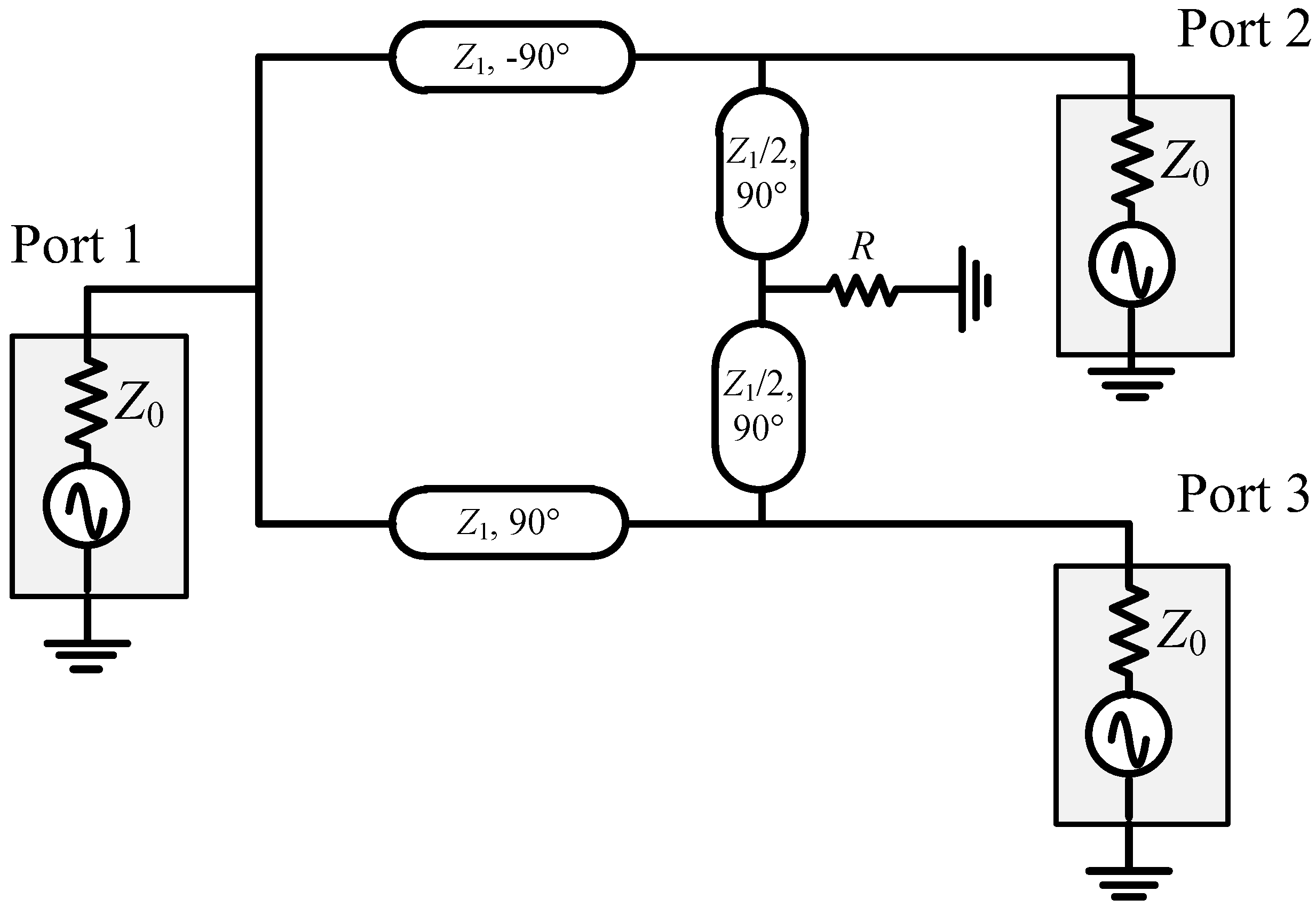
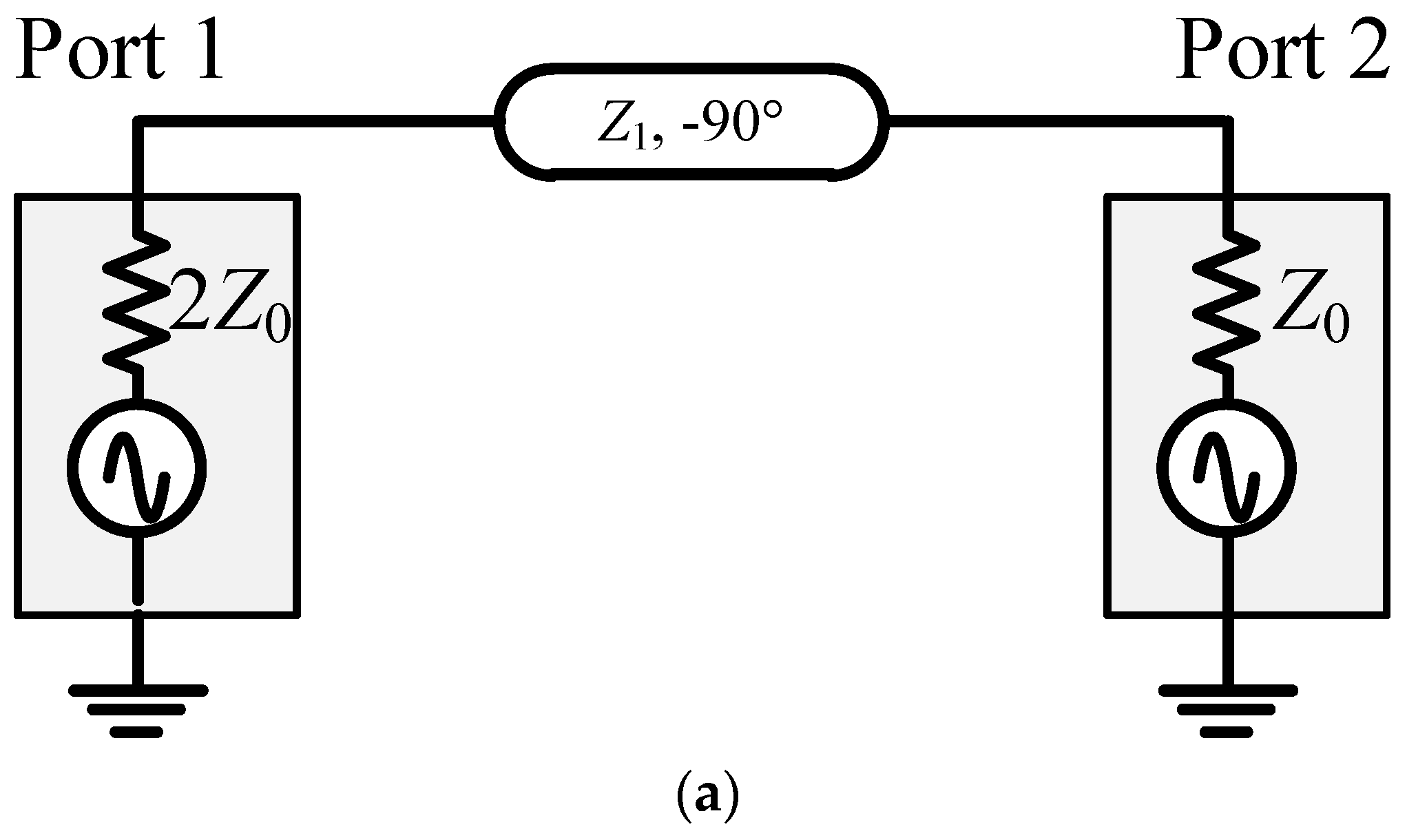
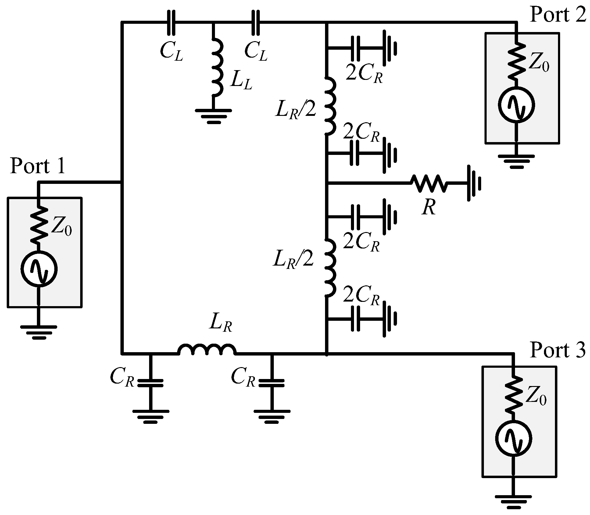
2. Conventional Wilkinson-Type Balun

Conventional Wilkinson-type baluns used transmission lines with opposite phases with distributed lines and a resistor placed between the output ports, as shown in Figure 1. The additional circuit branch between the output ports can be configurated in other forms as well [1,2]. Nevertheless, the distributed transmission lines in series branches must have the same characteristic impedance with an opposite phase. The even- and odd-mode circuits of the conventional Wilkinson-type balun are shown in Figure 2 and Figure 3.
For the even-mode circuits in Figure 2, the matching condition at both ports yield
Z 1 = 2 Z o
where Z 1 is the characteristic impedance of the transmission lines and Z 0 is the port impedance. For the odd-mode circuits in Figure 3, the matching condition at both ports yield
R = Z o 4
In CMOS implementation, the distributed transmission lines were replaced by lumped-transmission lines, e.g., right-handed or left-handed transmission lines [21]. The positive-phase transmission lines were replaced by right-handed transmission lines (RHTL), while the negative-phase transmission lines were replaced by left-handed transmission lines (LHTL). The lumped transmission line topologies use inductors and capacitors, as shown in Figure 4.
The inductor and capacitor values of the lumped transmission lines are related, as shown below.
L L = Z o ω sin θ
C L = sin θ ω Z o ( 1 cos θ )
L R = Z o ω 1 cos 2 θ
C R = 1 ω Z o 1 cos θ 1 + cos θ
where θ is the electrical length of the transmission line and ω is the angular frequency. Using the left- and right-handed transmission lines, the lumped transmission line balun circuit is shown in Figure 5.

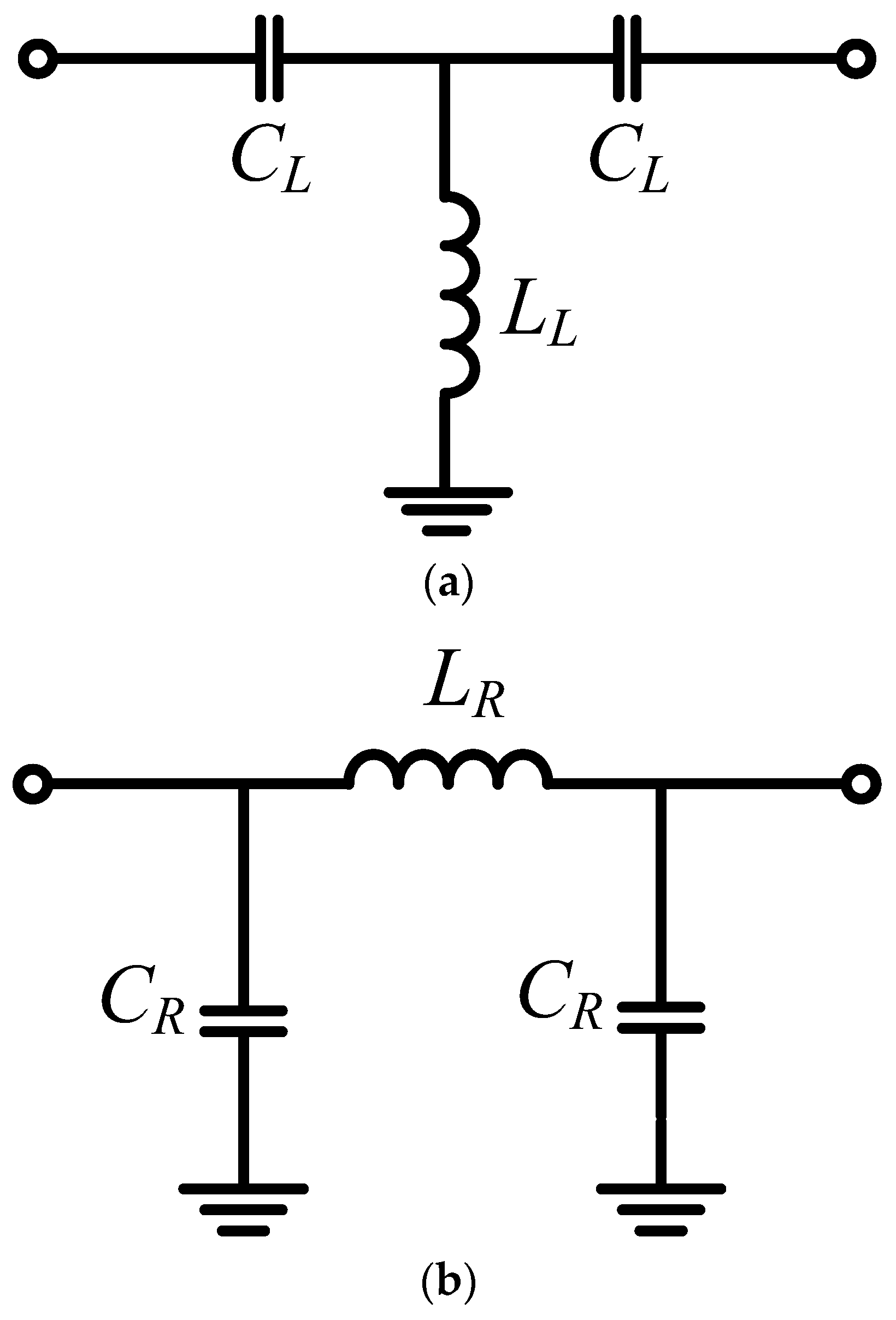
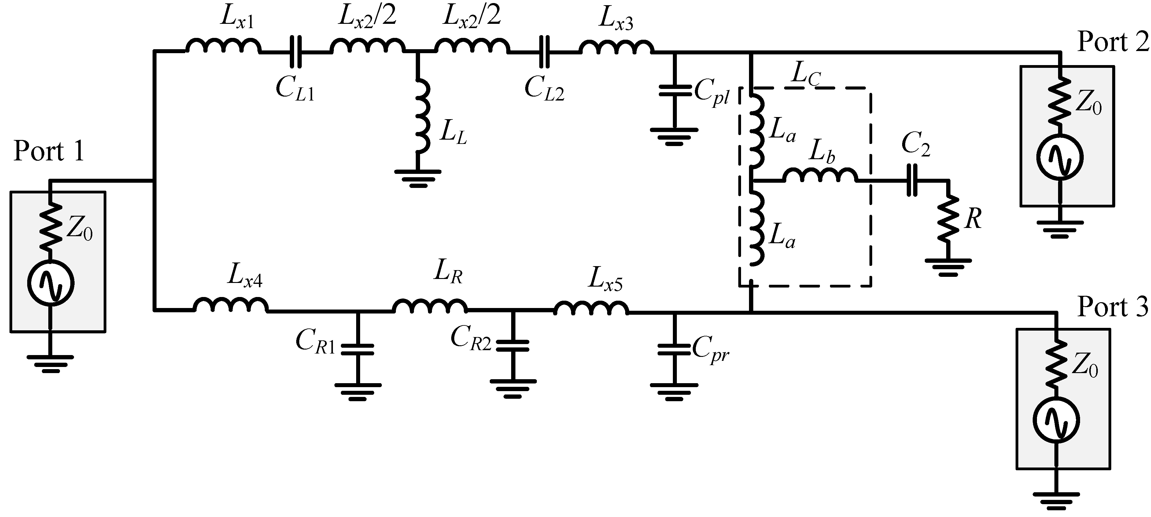
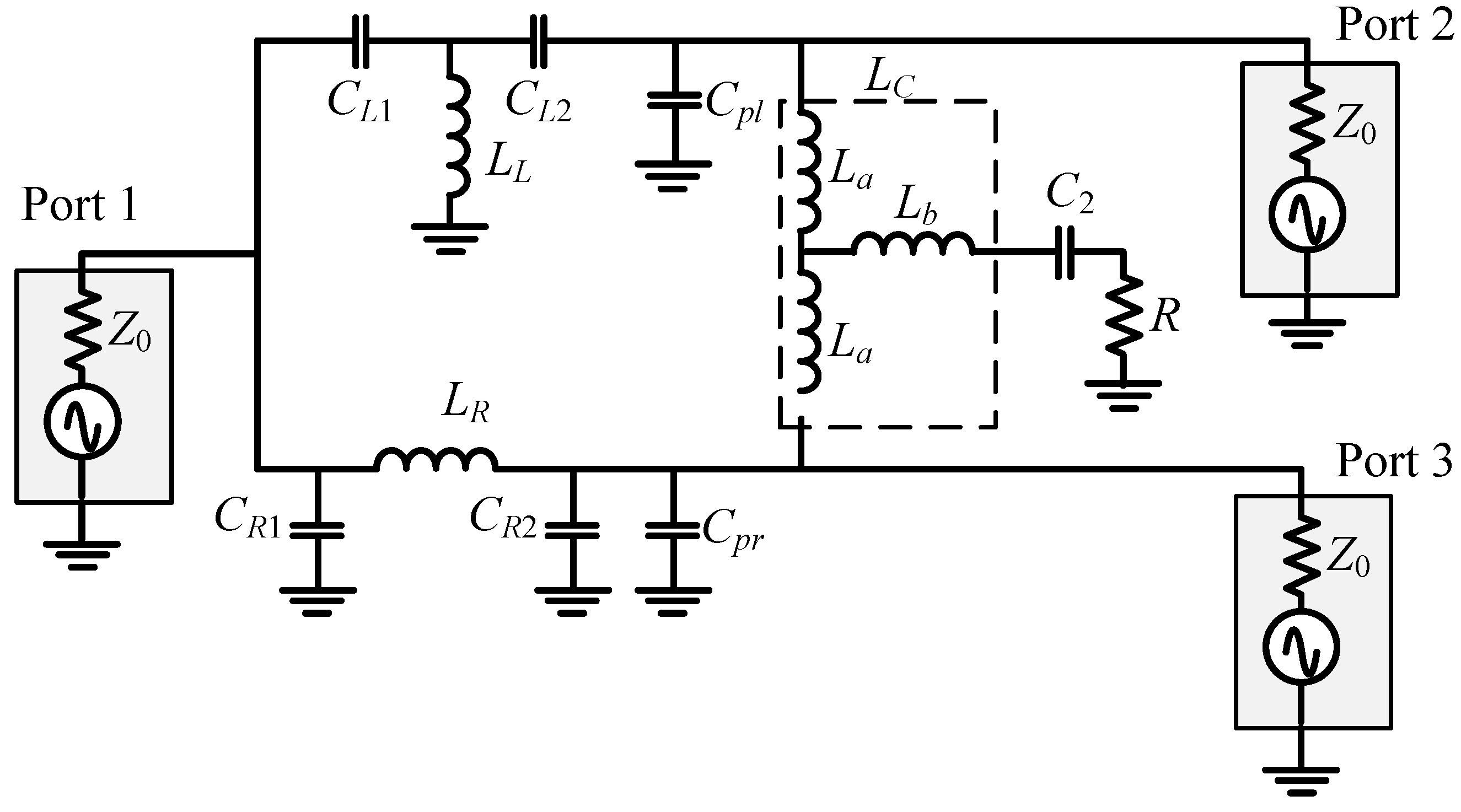
3. Balun with a Common Inductor

Figure 6 shows the proposed balun with a common inductor. The lumped transmission line balun was modified by replacing the transmission lines between the output Port 2 and Port 3 with a common inductor, a capacitor, and a resistor. Additional shunt capacitors were also added to the end of both left- and right-handed transmission lines. The capacitors of the left- and right-handed transmission lines were also modified to account for phase balance due to the resistive losses of the transmission lines. The effects of inductor losses will be discussed later.

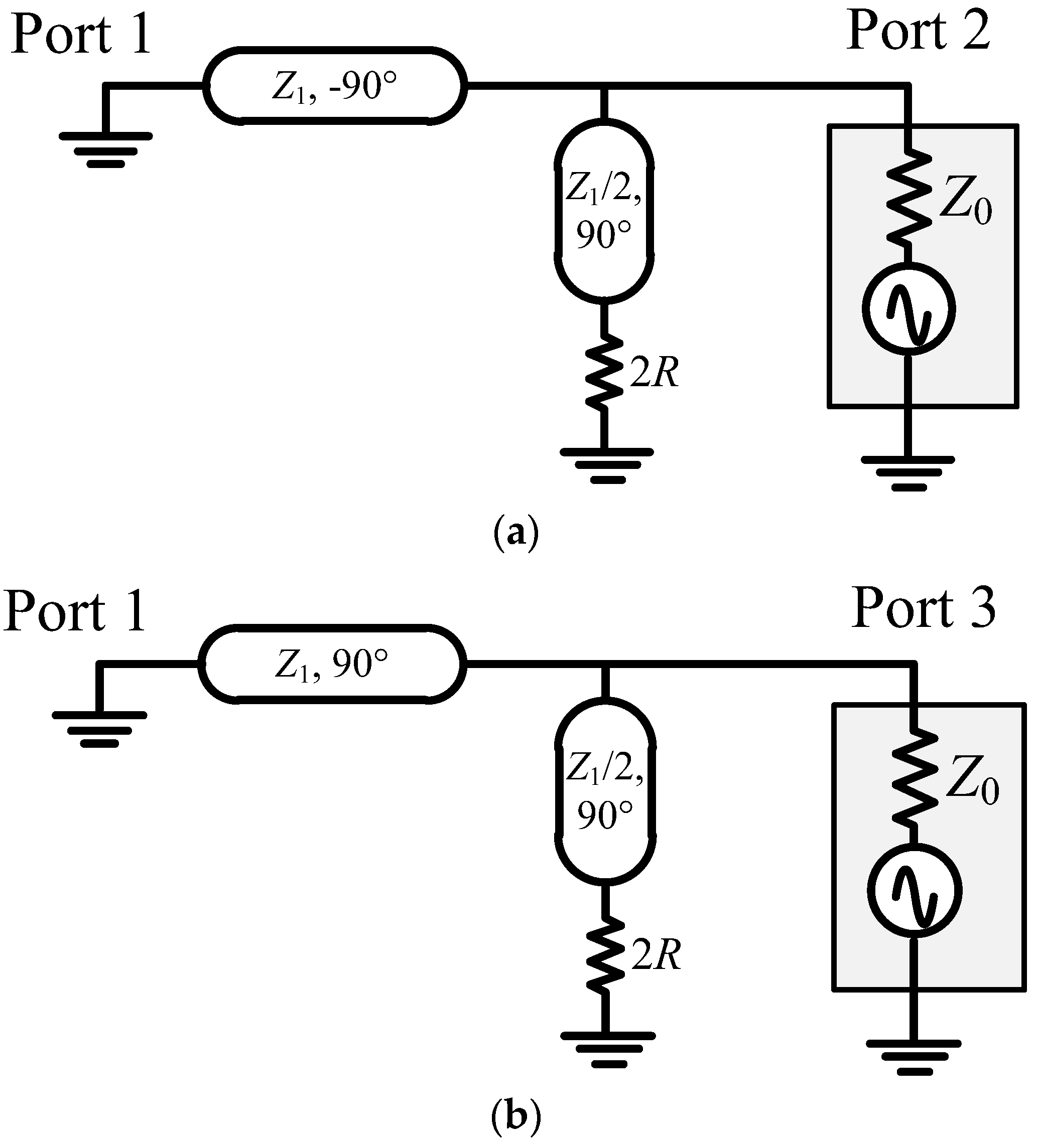
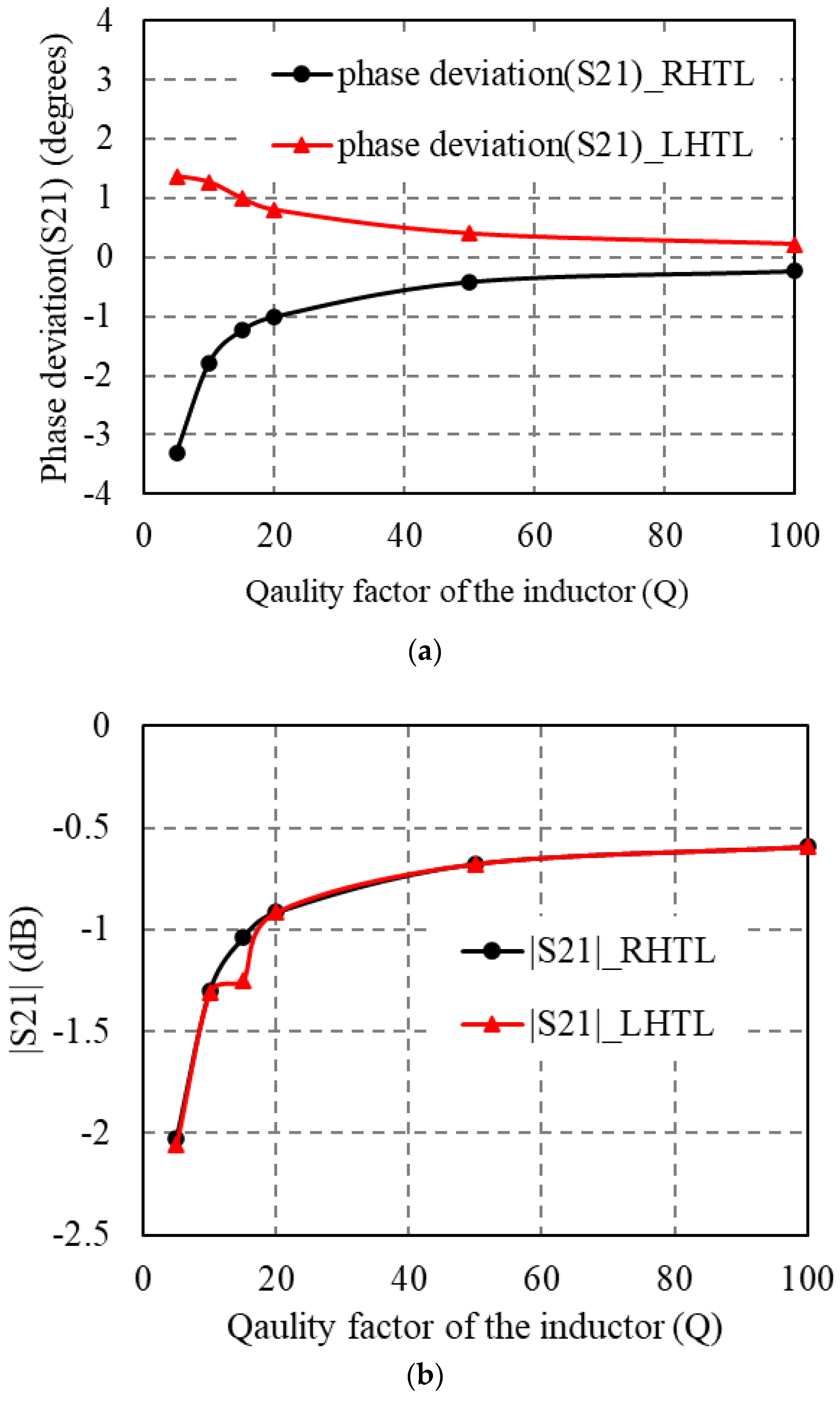
3.1. Phase Balance of Transmission Lines with Inductor Losses

In the CMOS process, the inductor losses were the main source of resistive losses of the circuit. The ideal lumped transmission line circuits, as shown in Figure 4, with the resistive losses in the inductor are discussed next. For a normal lumped transmission line circuit with ±90° electrical length at 10 GHz, the capacitors CL1, CL2, CR1, and CR2 are equal and chosen as 0.225 pF. The inductors LL and LR of the transmission lines have the same inductance as 1.125 nH. For an inductor, low resistive loss implies high quality factor values. Figure 7 shows the study of various quality factors (Q) of the inductors versus the transmission coefficient, S21. The phases of S21 are shown as the deviation from lossless transmission line ones, Δphase, as
Δ p h a s e = 90 p h a s e ( S 21 )   for   RHTL  
Δ p h a s e = p h a s e ( S 21 ) 90   for   LHTL
As the quality factor of the inductors lowered, the phase obtained more deviation from those of the lossless transmission lines. The lower Q inductor in the left-handed transmission line tends to increase the phase S21, while that in the right-handed transmission line tends to decrease the phase S21. Therefore, for a lower Q inductor, the differential phase between the transmission lines is less than 180°. For example, with a Q of 5, the right-handed transmission line has a phase S21 of −86.7° while the left-handed transmission line has a phase S21 of 91.37°. Then, the differential phase is only 178.07°.

3.2. Improvement of Phase Balance

To improve the phase balance of the circuit, the capacitors of the transmission lines are varied as CL1, CL2, CR1, and CR2. The impedances of inductors, LL and LR, are defined as
Z L L = R L + j ω L L
Z R R = R R + j ω L R
The impedance of each part (La and Lb) in the common inductor, LC, are defined as
Z a = R a + j ω L a
Z b = R b + j ω L b
The phase S21 of the left- ( θ s 21 , L H T L ) and right-handed transmission lines ( θ s 21 , R H T L ) are shown in (7).
θ S 21 , L H T L = tan 1 [ 1 R L 2 + ( ω L L ) 2 [ R L ω ( 1 C L 1 + 1 C L 2 ) + L L ω C L 1 C L 2 Z o ω L L Z o ] 1 ω Z o ( 1 C L 1 + 1 C L 2 ) 2 + ( 1 R L 2 + ( ω L L ) 2 ) [ R L Z o R L ω 2 C L 1 C L 2 Z o L L ( 1 C L 1 + 1 C L 2 ) ] ]
θ S 21 , L H T L = tan 1 [ ω R R ( C R 1 + C R 2 ) + ω L R Z o + ω Z o ( C R 1 + C R 2 ) ω 3 L R Z o C R 1 C R 2 2 + R R Z o [ R R Z o C R 1 C R 2 + L R ( C R 1 + C R 2 ) ] ω 2 ]
To impose the amplitude balance and phase balance of both transmission lines, the design equation becomes
| S 21 , L H T L | = | S 21 , R H T L |
| θ 21 , R H T L θ 21 , L H T L | = π
where S21,LHTL and S21, RHTL are shown in (9).
S 21 , L H T L = 2 2 + ( 1 R L + j ω L L ) [ 1 j ω ( 1 C L 1 + 1 C L 2 ) 1 ω 2 C L 1 C L 2 Z o + Z o ] + 1 j ω Z o ( 1 C L 1 + 1 C L 2 )
S 21 , R H T L = 2 2 + ( R R + j ω L R ) [ j ω ( C R 1 + C R 2 ) + 1 Z o Z o ω 2 C R 1 C R 2 ] + j ω Z o ( C R 1 + C R 2 )
With some choices of the capacitor selection in Table 1, the phase balance can be improved with some deteriorated S21 magnitudes.

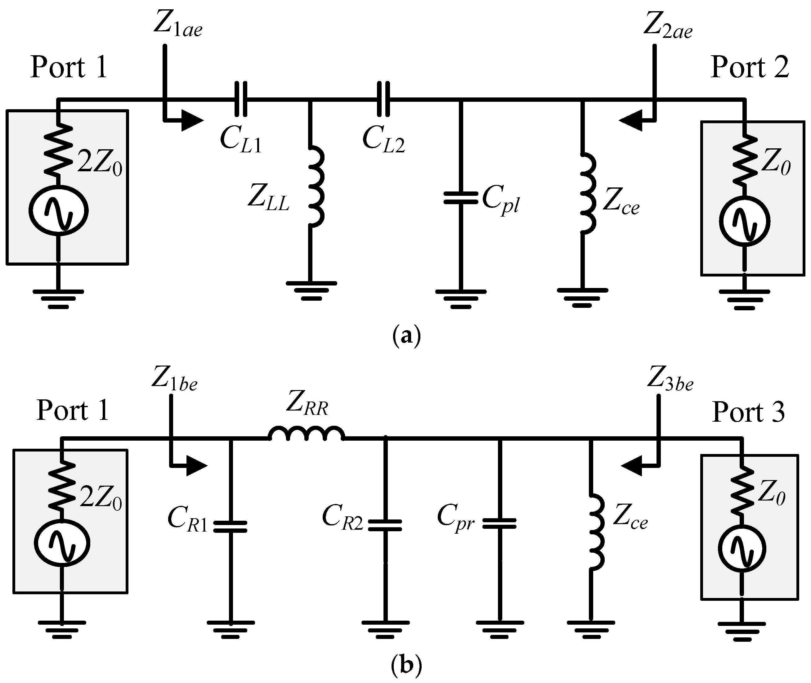
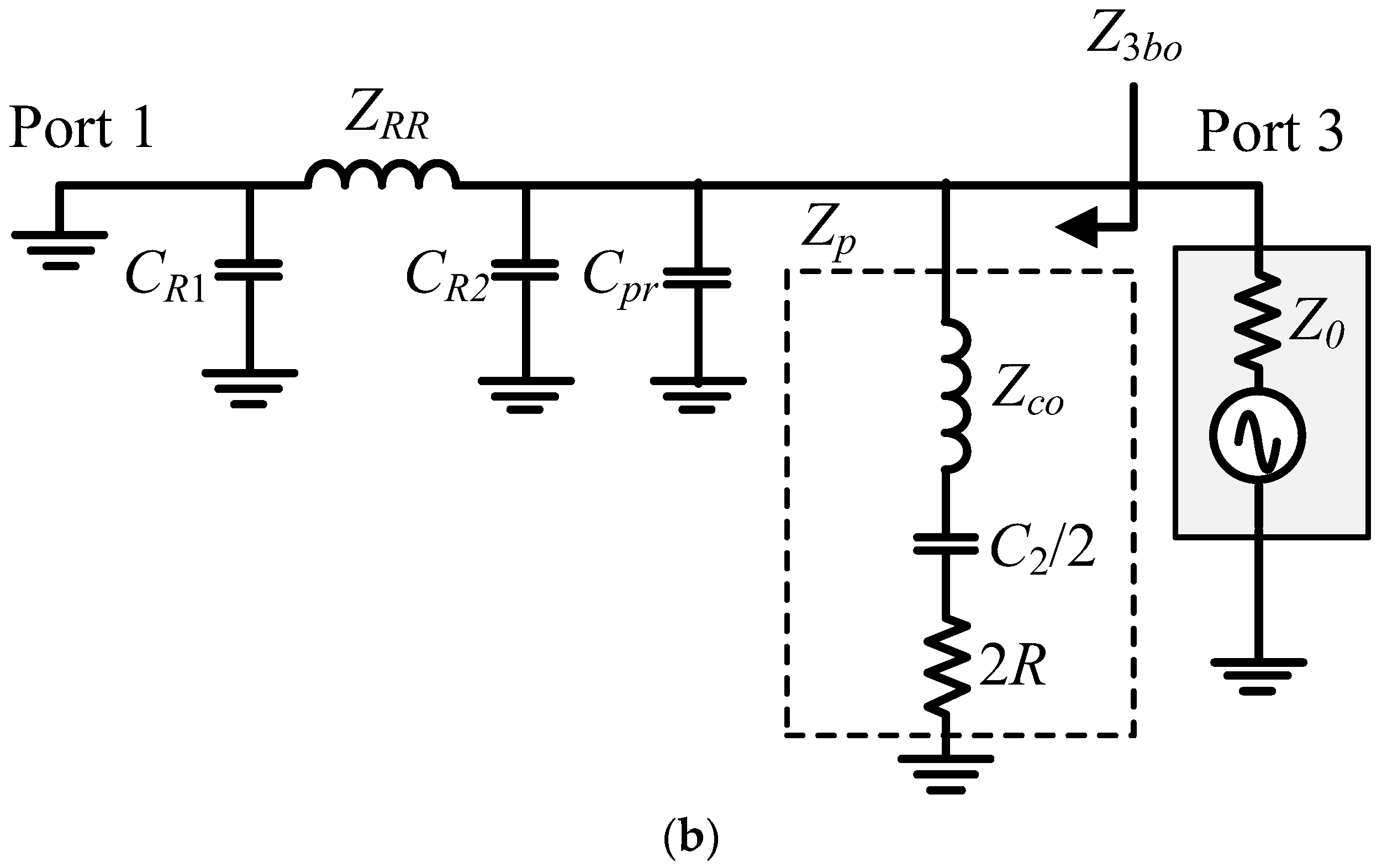
3.3. Even-Mode Analysis of Balun with Common Inductor

To analyze the balun circuit, an even/odd mode signal was excited to the balun. Then, the circuit could be analyzed separately with even- and odd-mode circuits, as shown in Figure 8 and Figure 9.
Equations (10)–(12) show the input impedance at each port, which is needed to match the port impedances. All capacitors are assumed to be lossless, while all inductors have inductive loss as their impedances are shown in (5) and (6).
Z 1 a e = 1 j ω C L 1 + ( R L + j ω L L ) { ( R a + j ω L a ) [ 1 + j ω Z 0 ( C p 1 + C L 2 ) ] + Z 0 } [ 1 + j ω C L 2 ( R L + j ω L L ) ] [ ( R a + j ω L a ) ( 1 + j ω Z 0 C p 1 ) + Z 0 ] + j ω Z 0 C L 2 ( R a + j ω L a )
Z 2 a e = ( R a + j ω L a ) [ ( 2 Z 0 + 1 j ω C L 1 ) ( R L + j ( ω L L 1 ω C L 2 ) ) + ( L L C L 2 j R L ω C L 2 ) ] ( 1 ω 2 C p 1 L a + j ω C p 1 R a ) [ ( 2 Z 0 + 1 j ω C L 1 ) ( R L + j ( ω L L 1 ω C L 2 ) ) + ( L L C L 2 j R L ω C L 2 ) ] + ( R a + j ω L a ) [ R L + 2 Z 0 + j ( ω L L 1 ω C L 1 ) ]
Z 1 b e = 1 + ( R R + j ω L R ) [ j ω ( C R 2 + C p r ) + 1 R a + j ω L a + 1 Z 0 ] j ω C R 1 + ( 1 ω 2 C R 1 L R + j ω C R 1 R R ) [ j ω ( C R 2 + C p r ) + 1 R a + j ω L a + 1 Z 0 ]
Z 2 b e = 2 Z 0 j ω C R 1 + ( R R + j ω L R ) ( 2 Z 0 + 1 j ω C R 1 ) 2 Z 0 + 1 j ω C R 1 + [ 2 Z 0 j ω C R 1 + ( R R + j ω L R ) ( 2 Z 0 + 1 j ω C R 1 ) ] [ j ω ( C R 2 + C p r ) + 1 R a + j ω L a ]
Z 2 a o = Z p [ R L ω 2 C p l ( C L 1 + C L 2 ) + j ( L L ω C p l ( C L 1 + C L 2 ) 1 ω 3 C p l ) ] [ L L ( C L 1 + C L 2 ) 1 ω 2 j R L ω ( C L 1 + C L 2 ) ] ( Z p + 1 j ω C p l ) + Z p C L 1 C L 2 ( L L C L 1 C L 2 C p l C L 2 ω 2 C p l j R L C L 1 C L 2 ω C p l )
Z 2 b o = Z p ( R R + j ω L R ) R R + j ω L R + Z p + j ω Z p ( C R 2 + C p r ) ( R R + j ω L R )
The impedances of the common inductor for the even mode, Z c e , and odd mode, Z c o , are
Z c e = R a + j ω L a
Z c o = R a + 2 R b + j ω ( L a + 2 L b )
The impedance of the parallel branch in Figure 9 is
Z p = j ω C 2 2 ω 2 C 2 ( L a + 2 L b ) + j ω C 2 ( R a + 2 R b + 2 R p )
In summary, the design equations are
Z 1 a e = 2 Z o
Z 2 a e = Z o
Z 1 b e = 2 Z o
Z 3 b e = Z o
Z 2 a o = Z o
Z 3 b o = Z o
which can be applied to find capacitors, inductors, and common inductor values.

4. Simulated and Measured Results

Balun circuits were designed to operate at 10 GHz. For the ideal lumped circuit simulation study, Equation (15) was applied to find optimum component values for fixed quality factor (Q) values of all inductors. The study used Q values of 1000, 100, and 10. Then, the balun circuit was designed and implemented on an 0.18-μm CMOS process. All the design component values are shown in Table 2. Design 1, 2, and 3 and parasitic components were found by using (15), while the ‘Layout’ components were found by using Advanced Design System (ADS) software (2014).
For the layout design, the common inductor was designed to have La = 1.926 nH and Lb = 0.11 nH. Figure 10 shows the chip photo. The size of the circuit is merely 1019 μm × 764 μm, or 0.025λ0 × 0.034λ0. In order to account for the layout effect, parasitic inductors were added to the circuit model, as shown in Figure 11. Design Equation (15) can still be applied with Equations (10)–(12), adjusted accordingly. Without loss of generality, the modified equations are not presented here but they can be easily found using the method described above. The estimated parasitic inductors at 10 GHz are shown in Table 3, while the designed components are shown in Table 2 as ‘Parasitic’.
For the layout, all other lumped components were adjusted using ADS to account for the parasitic parts of the layout. The inductors in both transmission lines were set at LL = LR = 0.953 nH. The capacitors of the left-handed transmission line were optimized to CL1 = 0.462 pF, CL2 = 0.265 pF, Cpl = 0.11 pF and those of the right-handed transmission line were CR1 = 0.1 pF, CR2 = 0.1 pF, Cpr = 0.276 pF. Because the optimized resistor R value was small, it was omitted from the circuit layout.
Figure 12 shows the comparison of |S11|, |S22|, |S33|, |S21|, |S31|, and |S23| of the simulated and measured results. The ideal circuits with different Q values are referred to as ‘Design Q = 1000’, ‘Design Q = 100’, ‘Design Q = 10’ and ‘Design_parasitic’. The layout simulation and measured results were referred to as ‘layout simulation’ and ‘measurement’. The measurement was performed by a Keysight network analyzer, Model N5247A.
For the ideal lump circuits, the performances of the baluns are similar to an ideal one if the quality factor of inductors is high, e.g., Q = 1000 and Q = 100. The balun performances worsen as the quality factor of the inductors is lower, Q = 10. The reflection coefficients rise with the lower Q inductors as port impedance matching worsens. The transmission coefficients are also lower because of signal loss on lossy components and impedance mismatch. The output signal coupling between the output ports also rises due to the port impedance mismatch. The simulation study results imply that the balun performance limitation is related to the quality factor of the inductors.
‘Design_parasitic’, ‘layout simulation’, and ‘measurement’ yielded similar performance to the ‘design Q = 10′. In particular, ‘Design_parasitic’ and ‘layout simulation’ were very close in all values at 10 GHz. For the design choices, ‘layout simulation’ just needed some adjustments from ‘Design_parasitic’, e.g., capacitor values, to account for the complex layout effect. The ‘measurement’ performance had A small deviation from ‘layout simulation’. The measured reflection coefficients of all ports were below −22.6 dB, while the simulated ones were below −17.8 dB. The measured transmission coefficients were more than −4.99 dB at both output ports. The measured phase difference at the output ports was 174.9°. Table 4 shows the comparison of this work with previously reported on-chip baluns.
In Table 4, the measurement of the proposed balun showed that the transmission coefficient was the best among other circuits based on lossy CMOS processes. It had the smallest size and amplitude balance among all circuits. Moreover, the reflection and isolation coefficients were all low. The measured results indicated good performance in narrowband applications.

5. Conclusions

The balun circuit was designed and implemented on a standard 0.18-μm CMOS process to operate at 10 GHz. The proposed topology uses left- and right-handed transmission lines to generate out-of-phase output signals at the output ports. With the modified lumped transmission line circuits, only single-section lines were used to replace λ/4 distributed transmission lines. A common inductor was also used to replace larger transmission line circuits. The resulting circuit was small at 1019 μm × 764 μm, or 0.025λ0 × 0.034λ0. It is convinced that the superior electrical performances and compact size of the design were suitable for narrowband applications.

Author Contributions

Conceptualization, C.P. and S.W.; methodology, C.P.; validation, C.P. and J.-L.X.; formal analysis, C.P.; investigation, C.P. and S.W.; resources, S.W.; writing—original draft preparation, C.P.; writing—review and editing, S.W.; visualization, C.P. and J.-L.X.; supervision, S.W.; project administration, C.P. and S.W.; funding acquisition, C.P. and S.W. All authors have read and agreed to the published version of the manuscript.

Funding

This research was funded by the Research Funding under the Memorandum of Understanding of King Mongkut’s Institute of Technology Ladkrabang, grant number KREF156501 and the National Taipei University of Technology-King Mongkut’s Institute of Technology Ladkrabang Joint Research Program (NTUT-KMITL), grant number NTUT-KMITL-110-01.

Data Availability Statement

Data sharing not applicable.

Acknowledgments

This work was supported in part by the College of Advanced Manufacturing Innovation, King Mongkut’s Institute of Technology Ladkrabang.

Conflicts of Interest

The authors declare no conflict of interest.

References

  1. Huynh, C.; Nguyen, C. Ultra-wideband active balun topology and its implementation on SiGe BiCMOS across DC-50 GHz. IEEE Microw. Wirel. Compon. Lett. 2016, 26, 720–722. [Google Scholar] [CrossRef]
  2. Huang, B.-J.; Huang, B.-J.; Lin, K.-Y.; Wang, H. A 2–40 GHz active balun using 0.13 μm CMOS process. IEEE Microw. Wirel. Compon. Lett. 2009, 19, 164–166. [Google Scholar] [CrossRef]
  3. Quan, X.; Zhuang, Y.; Li, Z.; Zhang, Y.; Jing, K. A 2–22GHz low-imbalanced active balun in 0.18μm SiGe BiCMOS technology. AEU Int. J. Electron. Commun. 2016, 70, 1367–1373. [Google Scholar] [CrossRef]
  4. Eskandari, R.; Ebrahimi, A.; Sobhi, J. A wideband noise cancelling balun LNA employing current reuse technique. Microelectron. J. 2018, 76, 1–7. [Google Scholar] [CrossRef]
  5. Manstretta, D. A broadband low-power low-noise active balun with second-order distortion cancellation. IEEE J. Solid-State Circuits 2012, 47, 407–420. [Google Scholar] [CrossRef]
  6. Chiang, H.-H.; Huang, F.-C.; Wang, C.-S.; Wang, C.-K. A 90 nm CMOS V-band low-noise active balun with broadband phase-correction technique. IEEE J. Solid-State Circuits 2011, 46, 2583–2591. [Google Scholar] [CrossRef]
  7. Chiou, H.-K.; Lin, J.-Y. Symmetric offset stack balun in standard 0.13-μm CMOS technology for three broadband and low-loss balanced passive mixer designs. IEEE Trans. Microw. Theory Techn. 2011, 59, 1529–1538. [Google Scholar] [CrossRef]
  8. Lin, Y.-S.; Lan, K.-S. Design and analysis of CMOS baluns for 94 GHz image radar and 28 GHz 5G communication system. Analog. Integr. Circ. Sig. Process 2020, 103, 435–450. [Google Scholar] [CrossRef]
  9. Yang, G.; Tang, K.; Wang, Z. 3.6–8.1 GHz CMOS balun with 1.8° in-band phase difference by using capacitive balance compensation technique. Microw. Opt. Technol. Lett. 2020, 62, 1548–1551. [Google Scholar] [CrossRef]
  10. Nithiporndecha, K.; Pakasiri, C. A UHF compact complex impedance-transforming balun with high isolation. Recent Adv. in Electr. Electron. Eng. 2020, 13, 1135–1144. [Google Scholar] [CrossRef]
  11. Frank, M.; Thorsell, M.; Enoksson, P. Design equations for lumped element balun with inherent complex impedance transformation. IEEE Trans. Microw. Theory Techn. 2017, 65, 5162–5170. [Google Scholar] [CrossRef]
  12. Ye, Y.; Li, L.-Y.; Gu, J.-Z.; Sun, X.-W. A bandwidth improved broadband compact lumped-element balun with tail inductor. IEEE Microw. Wirel. Compon. Lett. 2013, 23, 415–417. [Google Scholar] [CrossRef]
  13. Chiou, H.-K.; Lin, H.-H.; Chang, C.-Y. Lumped-element compensated high/low-pass balun design for MMIC double-balanced mixer. IEEE Microw. Wirel. Compon. Lett. 1997, 7, 248–250. [Google Scholar]
  14. Yeh, P.-C.; Liu, W.-C.; Chiou, H.-K. Compact 28-GHz subharmonically pumped resistive mixer MMIC using a lumped-element high-pass/band-pass balun. IEEE Microw. Wirel. Compon. Lett. 2005, 15, 62–64. [Google Scholar]
  15. Kumar, A.; Meng, F.-Y.; Wang, C.; Adhikari, K.K.; Qiang, T.; Wu, Q.; Wu, Y. Design analysis of integrated passive device-based balun devices with high selectivity for mobile application. IEEE Access 2019, 7, 23169–23176. [Google Scholar] [CrossRef]
  16. Cao, J.; Li, Z.; Li, Q.; Wang, Z. A wideband transformer balun with center open stub in CMOS process. IEEE Microw. Wirel. Compon. Lett. 2014, 24, 614–616. [Google Scholar] [CrossRef]
  17. Rotella, F.M.; Cismaru, C.; Tkachenko, Y.G.; Cheng, Y.; Zampardi, P.J. Characterization, design, modeling, and model validation of silicon on-wafer M:N balun components under matched and unmatched conditions. IEEE J. Solid-State Circuits 2006, 41, 1201–1209. [Google Scholar]
  18. Hsu, H.-M.; Huang, J.-S.; Chen, S.-Y.; Lai, S.-H. Design of an on-chip balun with a minimum amplitude imbalance using a symmetric stack layout. IEEE Trans. Microw. Theory Techn. 2010, 58, 814–819. [Google Scholar]
  19. Park, U. A Wilkinson-type balun using a composite right/left-handed transmission line. J.Inf. Commun. Converg. Eng. 2013, 11, 147–152. [Google Scholar] [CrossRef]
  20. Pakasiri, C.; Kongchayasukwat, T. Improvement of transmission line circuit on lossy substrate with application on phase shifter design. In Proceedings of the 2019 7th International Electrical Engineering Congress (iEECON), Hua Hin, Thailand, 6–8 March 2019. [Google Scholar]
  21. Caloz, C.; Itoh, T. Novel Microwave Devices and Structures Based on the Transmission Line Approach of Meta-Materials. IEEE MTT-S Int. Microw. Symp. Dig. 2003, 1, 195–198. [Google Scholar]
Figure 1. Schematic of the conventional Wilkinson−type balun.
Electronics 12 00468 g001
Figure 2. Schematic of the even−mode circuits between (a) Port 1 and Port 2 and (b) Port 1 and Port 3.
Electronics 12 00468 g002aElectronics 12 00468 g002b
Figure 3. Schematic of the odd−mode circuits between (a) Port 1 and Port 2 and (b) Port 1 and Port 3.
Electronics 12 00468 g003
Figure 4. Schematic of (a) left-handed and (b) right-handed transmission lines.
Electronics 12 00468 g004
Figure 5. Schematic of conventional lumped transmission line balun.
Electronics 12 00468 g005
Figure 6. Schematic of the balun with a common inductor.
Electronics 12 00468 g006
Figure 7. Magnitude and phase deviation of the left- and right-handed transmission lines. (a) Phase deviation of |S21| and (b) magnitude of |S21|.
Electronics 12 00468 g007
Figure 8. The even-mode circuits of balun with the common inductor between (a) Port 1 and Port 2 and (b) Port 1 and Port 3.
Electronics 12 00468 g008
Figure 9. The odd-mode circuits of balun with common inductor between (a) Port 1 and Port 2 and (b) Port 1 and Port 3.
Electronics 12 00468 g009aElectronics 12 00468 g009b
Figure 10. Balun circuit photo.
Electronics 12 00468 g010
Figure 11. Lumped balun circuit with parasitic inductors.
Electronics 12 00468 g011
Figure 12. Frequency response of the simulated and measured balun. (a) |S11|, (b) |S22|, (c) |S33|, (d) |S23|, (e) |S21|, (f) |S31|, (g) differential phase output.
Electronics 12 00468 g012aElectronics 12 00468 g012b
Table 1. Various balun designs for different Q values.
QCR1
(pF)
CR2
(pF)
CL1
(pF)
CL2
(pF)
|S21,LHTL|and |S21, RHTL| (dB)
50.160.330.180.33−2.46
100.290.170.190.29−1.49
200.190.280.290.17−1.10
500.180.280.200.27−0.82
1000.170.280.190.27−0.75
Table 2. Component values of various balun designs.
DesignLeft-Handed Transmission LineRight-Handed Transmission LineCommon InductorOther Components
CL1 (pF)CL2 (pF)LL
(nH)
Cpl (pF)CR1 (pF)CR2 (pF)LR
(nH)
Cpr (pF)La
(nH)
Lb
(nH)
C2
(pF)
Rp
(Ω)
1
(Q = 1000)
0.270.190.950.300.170.470.950.100.500.220.9412.87
2
(Q = 100)
2.990.231.130.240.220.511.130.160.570.240.757.97
3
(Q = 10)
0.420.261.190.100.210.111.190.241.930.110.2815.00
Parasitic0.2680.3620.9530.30.310.140.9530.4111.9260.110.290.1
Layout0.4620.2650.9530.110.100.100.9530.2761.9260.110.246-
Table 3. Estimated parasitic inductors from the layout at 10 GHz.
Parasitic Inductor Resistance (Ω)Inductance (nH)
Lx10.2730.072
Lx20.3190.012
Lx31.2460.142
Lx40.3710.038
Lx50.9350.09
Table 4. Comparison of previously reported on-chip baluns.
Refs.[2]
Balun
[2]
Miniature Balun
[8][15]This Work
Process0.18 μm CMOS0.18 μm CMOS0.18 μm CMOSIPD0.18 μm CMOS
f0(GHz)37.836.9942.410
|S21|, |S31|(dB)>−6.281>−5.809>−6.178−3.25>−4.99
|S11|, |S22|, |S33| (dB)<−9.6<−14.5<−6.3−21<−17.8
|S23|
(dB)
−20.9−16.8−6 *N/A<−16.8
Amplitude balance (dB)1.2270.6370.0980.450.045
Phase difference deviation
(degrees)
00−4.92.65.1
Size
0 × λ0)
1.1 × 10−31×10−33.5 × 10−31.12 × 10−38.662 × 10⁻⁴
* Estimation.
Disclaimer/Publisher’s Note: The statements, opinions and data contained in all publications are solely those of the individual author(s) and contributor(s) and not of MDPI and/or the editor(s). MDPI and/or the editor(s) disclaim responsibility for any injury to people or property resulting from any ideas, methods, instructions or products referred to in the content.

