Abstract
Recently, hybrid logic circuits based on magnetic tunnel junctions (MTJs) have been widely investigated to realize zero standby power. However, such hybrid CMOS/MTJ logic circuits suffer from a severe sensing reliability due to the limited tunnel magnetoresistance ratio (TMR ≤ 150%) of the MTJ and the large process variation in the deep sub-micrometer technology node. In this paper, a novel differential sensing amplifier (DSA) is proposed, in which two PMOS transistors are added to connect the discharging branches and evaluation branches. Owing to the positive feedback realized by these two added PMOS transistors, it can achieve a large sensing margin. By using an industrial CMOS 40 nm design kit and a physics-based MTJ compact model, hybrid CMOS/MTJ simulations have been performed to demonstrate its functionality and evaluate its performance. Simulation results show that it can achieve a smaller sensing error rate of 9% in comparison with the previously proposed DSAs with a TMR ratio of 100% and process variation of 10%, while maintaining almost the same sensing delay of 74.5 ps and sensing energy of 1.92 fJ/bit.
1. Introduction
As the technology node continuously scales down, CMOS-based logic circuits suffer from high standby power consumption induced by the increasing leakage current. To address this issue, many new nanodevices and structures have been presented recently to realize zero standby power [1,2,3]. Among them, the MTJ is preferable, because of its high speed, long data retention, nearly infinite endurance, great scalability and good compatibility with CMOS process technology, in comparison with other eNVM devices [4,5,6]. Figure 1a illustrates the structure of an MTJ device composed of two ferromagnetic (FM) layers (e.g., CoFeB) separated by one oxide barrier layer (e.g., MgO). Generally, the magnetization direction of the FM layer (which is called a free layer) is fixed; the magnetization direction of the other FM layer (which is called the pinning layer) can be reversed. Depending on the relative magnetization orientation of these two FM layers, i.e., parallel (P) or anti-parallel (AP), each MTJ device can exhibit two stable resistance states, i.e., RP or RAP, which are used to represent binary logic information ‘0′ and ‘1′, respectively, as shown in Figure 1b. Using the MTJs as the non-volatile storage elements, several non-volatile logic circuits, such as magnetic flip-flop [7,8,9], magnetic look-up table [10,11,12], magnetic full-adder [13,14,15] and ternary content-addressable memory [16,17,18], have been proposed.
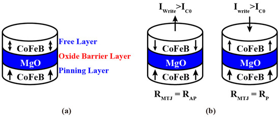
Figure 1.
(a) Structure schematic of Magnetic Tunnel Junction (MTJ). (b) Spin Transfer Torque (STT) writing mechanism.
One critical issue in these hybrid CMOS/MTJ logic circuits is to correctly sense the information stored in the MTJ [19,20,21,22,23]. So far, various DSAs have been proposed, in which two MTJs with opposite resistance states are employed to represent one bit. For example, the pre-charge sensing amplifier (PCSA) circuit [24], as shown in Figure 2a, can achieve high sensing reliability (10–5 at 90 nm), small sensing delay (~125 ps) and low sensing energy (~1 fJ/bit). However, as the CMOS technology shrinks below 45 nm, the sensing reliability gets worse and worse (e.g., 79% at 40 nm) due to the increased process variation. To overcome this issue, a separated PCSA (SPCSA) [25] is proposed as shown in Figure 2b, which can improve the sensing reliability (82% at 40 nm) while retaining high sensing speed and low sensing energy dissipation. However, its sensing margin is still limited due to the small TMR ratio of the MTJ. To improve the sensing margin, a reliability-enhanced SPCSA (RESPCSA) [26] is proposed as shown in Figure 2c, which can further improve the sensing reliability (84% at 40 nm). However, it is still not sufficient for reliable logic circuits. This paper proposes a novel differential sensing amplifier based on the RESPCSA, in which two PMOS transistors are added to connect the discharging branches and evaluation branches. By using the positive feedback of two PMOS transistors, the proposed DSA is envisioned to obtain a large sensing margin, thereby achieving high sensing reliability.
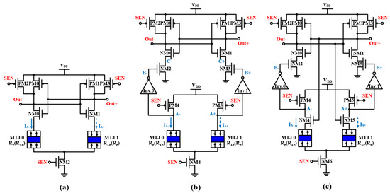
Figure 2.
Schematics of (a) PCSA [24] (b) SPCSA [25] and (c) RESPCSA [26].
2. Proposed Reliability-Enhanced Differential Sensing Amplifier Circuit
Figure 3 shows the proposed reliability-enhanced differential sensing amplifier (REDSA) circuit. Similar to the previous RESPCSA, the proposed REDSA also includes three operation phases, i.e., pre-charging phase, discharging phase and evaluation phase, depending on the control signal “SEN”. From the perspective of the circuit configuration, the main difference is that two PMOS transistors PM4 and PM5 are added to connect the discharging branches and evaluation branches. As a result, two positive feedback loops can be formed and a large sensing margin can be achieved, which will be demonstrated in Section 3. The sensing operation is described as follows.
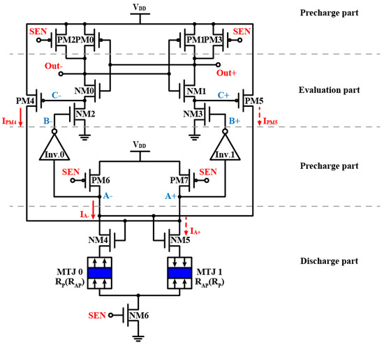
Figure 3.
Schematic of the proposed sensing amplifier.
When the “SEN” is set to ‘0′, the proposed REDSA enters the pre-charging phase. PM2–PM3 and PM6–PM7 turn on and the NMOS transistor NM6 is in the off state. As a result, the nodes A (A+ and A-), C (C+ and C-) and Out (Out+ and Out-) are charged to VDD. When the “SEN” goes to ‘1′, the proposed REDSA goes into the discharging phase. NM6 turns on, and both the nodes A+ and A- begin to discharge, but with different speeds due to the resistance difference between their individual discharging branches, resulting in a voltage difference (ΔVA) between them. Then, the ΔVA can be inversely amplified by both the inverter 0 (Inv.0) and Inv.1, which enables the nodes Out+ and Out- to discharge with different speeds as well as the nodes C+ and C-, leading to a voltage differenceΔVOut and a voltage difference ΔVC. The voltage difference ΔVC can in turn enlarge the ΔVA thanks to the positive feedback of PM4 and PM5. Once one of the nodes Out+ and Out- becomes less than the threshold voltage of the cross-coupled inverters (composed of PM0–NM0 and PM1–NM1), the proposed REDSA enters into the evaluation phase. Finally, one of the nodes Out+ and Out- will continue discharging to GND, while the other will eventually charge to VDD. For example, when MTJ0 is in a high resistance (RAP) state and MTJ1 in a low resistance (RP) state, the node Out+ will be discharged to GND and the node Out- will be charged to VDD and vice versa.
3. Functional Verification
By using a physics-based MTJ compact model [27,28,29,30] and an industrial CMOS 40 nm design kit, hybrid CMOS/MTJ simulations have been performed to demonstrate its functionality and evaluate its performance. The key parameters of the compact MTJ model are listed in Table 1.

Table 1.
The Key Parameters of the MTJ in Simulations.
Figure 4a shows the transient simulation waveforms of the proposed REDSA, where the MTJ0 is in a low resistance state and the MTJ1 in a high resistance state. As seen, during the pre-charging phase (“SEN” = 0 V), the nodes (A+, A-) and (Out+, Out-) are charged to VDD. When the “SEN” rises to ‘1′, they enter the discharging phase, and the nodes A+ and A- begin to discharge but with different speeds, resulting in a voltage difference ΔVA. Owing to the positive feedback of the two added PMOS transistors, the ΔVA is enlarged after the point Ml (or M2). Then, this enlarged ΔVA is amplified, inducing a large voltage difference ΔVOut. As a result, the node Out- firstly becomes less than the threshold of the cross-coupled inverters. Then, the proposed REDSA enters into the evaluation phase, the node Out- continues discharging after the point M10 and the Out+ is charged after the point M9. As seen, the proposed REDSA can achieve a large sensing margin of 732.6 mV (the voltage difference between the points M9 and M10) and a small sensing delay of 74.5 ps (taken from the points M0 to M11). Since the sensing delay is less 75 ps, it can work with a high clock frequency, up to 6.7 GHz. Figure 4b confirms that there is no static current during the sensing operation, only dynamic charging and discharging current. The total power per bit sensing operation of the proposed REDSA is about 1.92 fJ.
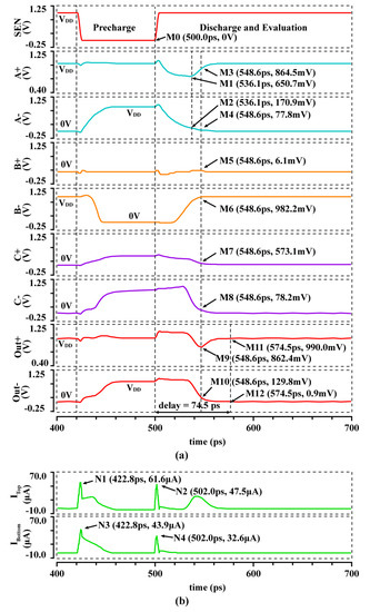
Figure 4.
(a) Transient voltage simulation waveforms of the proposed REDSA. (b) Currents that flow through the proposed REDSA.
4. Performance Analysis and Comparison
4.1. Reliability Analysis and Comparative Discussion
Firstly, this paper investigates the sensing margin of the proposed REDSA with respect to different supply voltages. As shown in Figure 5a, with the increase of the supply voltage, its sensing margin can be improved. Compared to the previous RESPCSA in [17], the proposed REDSA can achieve a very larger sensing margin, even with a small supply voltage. For example, the sensing margin can reach 696 mV when the supply voltage is 0.8 V, while it is only about 280 mV for the RESPCSA. The influence of the TMR ratio on the sensing margin is also investigated, as shown in Figure 5b. As seen, the sensing margin increases with the increase of the TMR ratio. However, even with a small TMR ratio of 50%, the sensing margin of the proposed REDSA can reach up to 632 mV, which is much larger than that of the RESPCSA.
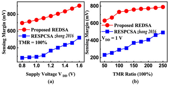
Figure 5.
Comparison of the sensing margin of the proposed REDSA and the RESPCSA with respect to different supply voltages (a) and TMR ratios (b) [17].
To evaluate the sensing reliability of the proposed REDSA quantitatively, Monte Carlo statistical simulations (1000 runs per case) have been performed with consideration of the 1σ probability distributions of the CMOS transistors fixed by the CMOS process manufacturer and the 3% process variations of MTJ, including TMR ratio, free layer thickness and oxide barrier thickness. Figure 6a shows the impact of the device variation on the sensing error rate (SER), where the TMR ratio is 100%. As seen, the proposed REDSA exhibits a greater tolerance to device variation in comparison with the RESPCSA. Additionally, the SER with respect to the TMR ratio is evaluated, as shown in Figure 6b. As seen, the proposed REDSA can provide a much higher sensing reliability in comparison to the RESPCSA when the TMR ratio is less than 150%.
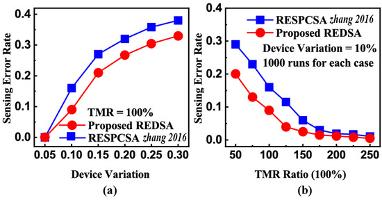
Figure 6.
Comparison of the sensing error rate of proposed REDSA and the RESPCSA with respect to different device variation (a) and TMR ratios (b) [17].
4.2. Layout of the Proposed REDSA
A hybrid CMOS/MTJ process can be used to fabricate MTJs as they can be embedded above CMOS circuits. As shown in Figure 7a, the MTJ device can be fabricated between the third metal level (M3) and the fourth metal level (M4) using a 3D back-end integration process. Figure 7b shows the standard cell for one logic bit, which is composed of two complementary MTJs. The MTJ bottom electrode connects to the third metal level (M3) and the MTJ top electrode connects to the fourth metal level (M4). Figure 7c shows the layout of the proposed REDSA, which is drawn with the 40 nm layout design rules. The effective area of the proposed REDSA is about 16.48 μm2.
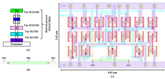
Figure 7.
(a) The MTJ nano-pillar is implemented above the CMOS logic circuit with a 3D back-end integration process between the third metal level (M3) and the fourth metal level (M4). (b) The standard cell for one logic bit, which is composed of two complementary MTJs. (c) Layout of the proposed REDSA, where the two MTJs in the layout are marked out in the figure.
4.3. Performance Comparison
Table 2 summarizes the performance comparison of the proposed REDSA and the previous DSAs. As seen, compared to the previous DSAs, the proposed REDSA can achieve a smaller sensing error rate, while retaining almost the same sensing delay of 74.5 ps and sensing energy of 1.92 fJ per bit. Although the main drawback of the proposed REDSA is its relatively larger area, multiple non-volatile memory cells can share one sensing amplifier by using multi-context hybrid CMOS/MTJ logic circuits [31,32].
Table 2.
Performance comparison with TMR Ratio of 100% and Process Variation of 10%.
5. Conclusions
In this paper, a novel reliability-enhanced differential sensing amplifier with a large sensing margin is proposed to realize high reliability. Hybrid CMOS/MTJ simulation results show that it can achieve a smaller sensing error rate of 9% than that of the previous differential sensing amplifiers, while retaining almost the same sensing delay of 74.5 ps and sensing energy of 1.92 fJ/bit. The proposed REDSA will assist in the design of low-power and high-reliability nonvolatile SRAMs in battery operated sensor nodes and Internet of Things (IoT) applications.
Author Contributions
Conceptualization, C.W.; methodology, D.W.; software, C.W.; validation, C.W., T.Y., M.H. and D.W.; formal analysis, T.Y.; investigation, D.W.; resources, M.H.; data curation, T.Y.; writing—original draft preparation, T.Y.; writing—review and editing, M.H.; visualization, M.H.; supervision, T.Y.; project administration, D.W.; funding acquisition, C.W. and M.H. All authors have read and agreed to the published version of the manuscript.
Funding
This research was funded by the National Natural Science Foundation of China under Grant 62104259 and Grant 61802427.
Institutional Review Board Statement
Not applicable.
Informed Consent Statement
Not applicable.
Data Availability Statement
Conflicts of Interest
The authors declare no conflict of interest.
References
- Banerjee, W. Challenges and Applications of Emerging Nonvolatile Memory Devices. Electronics 2020, 9, 1029. [Google Scholar] [CrossRef]
- Swami, S.; Mohanram, K. Reliable Nonvolatile Memories: Techniques and Measures. IEEE Des. Test 2017, 34, 31–41. [Google Scholar] [CrossRef]
- Thapliyal, H.; Sharifi, F.; Kumar, S.D. Energy-Efficient Design of Hybrid MTJ/CMOS and MTJ/Nanoelectronics Circuits. IEEE Trans. Magn. 2018, 54, 1–8. [Google Scholar] [CrossRef]
- Chen, Y. ReRAM: History, status, and future. IEEE Trans. Electron Devices 2020, 67, 1420–1433. [Google Scholar] [CrossRef]
- Fantini, P. Phase change memory applications: The history, the present and the future. J. Phys. D Appl. Phys. 2020, 53, 283002. [Google Scholar] [CrossRef]
- Dieny, B.; Prejbeanu, I.L.; Garello, K.; Gambardella, P.; Freitas, P.; Lehndorff, R.; Raberg, W.; Ebels, U.; Demokritov, S.O.; Akerman, J.; et al. Opportunities and challenges for spintronics in the microelectronics industry. Nat. Electron. 2020, 3, 446–459. [Google Scholar] [CrossRef]
- Amirany, A.; Jafari, K.; Moaiyeri, M.H. High-Performance Spintronic Nonvolatile Ternary Flip-Flop and Universal Shift Register. IEEE Trans. Very Large Scale Integr. (VLSI) Syst. 2021, 29, 916–924. [Google Scholar] [CrossRef]
- Amirany, A.; Marvi, F.; Jafari, K.; Rajaei, R. Nonvolatile Spin-Based Radiation Hardened Retention Latch and Flip-Flop. IEEE Trans. Nanotechnol. 2019, 18, 1089–1096. [Google Scholar] [CrossRef]
- Natsui, M.; Yamagishi, G.; Hanyu, T. Design of a highly reliable nonvolatile flip-flop incorporating a common-mode write error detection capability. Jpn. J. Appl. Phys. 2021, 60, SBBB02. [Google Scholar] [CrossRef]
- Suzuki, D.; Hanyu, T. Design of a highly reliable, high-speed MTJ-based lookup table circuit using fractured logic-in-memory structure. Jpn. J. Appl. Phys. 2019, 58, SBBB10. [Google Scholar] [CrossRef]
- Jamshidi, V. NVRH-LUT: A nonvolatile radiation-hardened hybrid MTJ/CMOS-based look-up table for ultralow power and highly reliable FPGA designs. Turk. J. Electr. Eng. Comput. Sci. 2019, 27, 4486–4501. [Google Scholar] [CrossRef]
- Zhang, H.; Kang, W.; Wang, Z.; Deng, E.; Zhang, Y.; Zhao, W. High-density and fast-configuration non-volatile look-up table based on NAND-like spintronic memory. In Proceedings of the 2018 IEEE Asia Pacific Conference on Circuits and Systems (APCCAS), Chengdu, China, 26–30 October 2018; pp. 382–385. [Google Scholar] [CrossRef]
- Shukla, P.; Kumar, P.; Misra, P.K. A Highly Reliable, Dynamic Logic-Based Hybrid MTJ/CMOS Magnetic Full Adder for High-Performance and Low-Power Application. IEEE Trans. Magn. 2022, 58, 1–8. [Google Scholar] [CrossRef]
- Bae, G.Y.; Hwang, Y.; Lee, S.; Kim, T.; Park, W. Reconfigurable logic for carry-out computing in 1-bit full adder using a single magnetic tunnel junction. Solid-State Electron. 2019, 154, 16–19. [Google Scholar] [CrossRef]
- Deng, E.; Zhang, Y.; Kang, W.; Dieny, B.; Klein, J.-O.; Prenat, G.; Zhao, W. Synchronous 8-bit Non-Volatile Full-Adder based on Spin Transfer Torque Magnetic Tunnel Junction. IEEE Trans. Circuits Syst. I Regul. Pap. 2015, 62, 1757–1765. [Google Scholar] [CrossRef]
- Wang, C.; Zhang, D.; Zeng, L.; Zhao, W. Design of Magnetic Non-Volatile TCAM With Priority-Decision in Memory Technology for High Speed, Low Power, and High Reliability. IEEE Trans. Circuits Syst. I Regul. Pap. 2019, 67, 464–474. [Google Scholar] [CrossRef]
- Wang, C.; Zhang, D.; Zeng, L.; Deng, E.; Chen, J.; Zhao, W. A Novel MTJ-Based Non-Volatile Ternary Content-Addressable Memory for High-Speed, Low-Power, and High-Reliable Search Operation. IEEE Trans. Circuits Syst. I: Regul. Pap. 2018, 66, 1454–1464. [Google Scholar] [CrossRef]
- Arakawa, R.; Onizawa, N.; Diguet, J.-P.; Hanyu, T. Multi-Context TCAM-Based Selective Computing: Design Space Exploration for a Low-Power NN. IEEE Trans. Circuits Syst. I: Regul. Pap. 2020, 68, 67–76. [Google Scholar] [CrossRef]
- Natsui, M.; Suzuki, D.; Tamakoshi, A.; Watanabe, T.; Honjo, H.; Koike, H.; Nasuno, T.; Ma, Y.; Tanigawa, T.; Noguchi, Y.; et al. 12.1 An FPGA-Accelerated Fully Nonvolatile Microcontroller Unit for Sensor-Node Applications in 40nm CMOS/MTJ-Hybrid Technology Achieving 47.14 μW Operation at 200 MHz. In Proceedings of the 2019 IEEE International Solid-State Circuits Conference (ISSCC), San Francisco, CA, USA, 17–21 February 2019; pp. 202–204. [Google Scholar]
- Zheng, S.W.; Bi, J.S.; Xi, K.; Liu, J.; Liu, M.; Luo, L. A 28 nm full-margin, high-reliability, and ultra-low-power consumption sense amplifier for STT-MRAM. Microelectron. Reliab. 2019, 100–101, 113465. [Google Scholar] [CrossRef]
- Chen, J.; Yin, N.; Yu, Z. High speed, Low Resource and Non-volatile MTJ-CMOS Hybrid Logical Circuits. In Proceedings of the 2018 14th IEEE International Conference on Solid-State and Integrated Circuit Technology (ICSICT), Qingdao, China, 31 October–3 November 2018; pp. 1–3. [Google Scholar] [CrossRef]
- Kumar, S.D.; Thapliyal, H. Exploration of non-volatile MTJ/CMOS circuits for DPA-resistant embedded hardware. IEEE Trans. Magn. 2019, 55, 1–8. [Google Scholar] [CrossRef]
- Cai, H.; Han, M.; Wang, Y.; Naviner, L.; Liu, X.; Yang, J.; Zhao, W. Reliability emphasized MTJ/CMOS hybrid circuit towards ultra-low power. In Proceedings of the 2018 Conference on Design of Circuits and Integrated Systems (DCIS), Lyon, France, 14–16 November 2018; pp. 1–5. [Google Scholar] [CrossRef]
- Zhao, W.; Chappert, C.; Javerliac, V.; Noziere, J.-P. High Speed, High Stability and Low Power Sensing Amplifier for MTJ/CMOS Hybrid Logic Circuits. IEEE Trans. Magn. 2009, 45, 3784–3787. [Google Scholar] [CrossRef]
- Kang, W.; Deng, E.; Klein, J.-O.; Zhang, Y.; Zhang, Y.; Chappert, C.; Ravelosona, D.; Zhao, W. Separated Precharge Sensing Amplifier for Deep Submicrometer MTJ/CMOS Hybrid Logic Circuits. IEEE Trans. Magn. 2014, 50, 1–5. [Google Scholar] [CrossRef]
- Zhang, D.; Zeng, L.; Zhang, Y.; Klein, J.O.; Zhao, W. Reliability-Enhanced Hybrid CMOS/MTJ Logic Circuit Architecture. IEEE Trans. Magn. 2017, 53, 1–5. [Google Scholar] [CrossRef]
- Wang, Y.; Cai, H.; de Barros Naviner Naviner, L.A.; Zhang, Y.; Zhao, X.; Deng, E.; Klein, J.-O.; Zhao, W. Compact Model of Dielectric Breakdown in Spin-Transfer Torque Magnetic Tunnel Junction. IEEE Trans. Electron Devices 2016, 63, 1762–1767. [Google Scholar] [CrossRef]
- Zhang, Y.; Zhao, W.; Lakys, Y.; Klein, J.-O.; Kim, J.-V.; Ravelosona, D.; Chappert, C. Compact Modeling of Perpendicular-Anisotropy CoFeB/MgO Magnetic Tunnel Junctions. IEEE Trans. Electron Devices 2012, 59, 819–826. [Google Scholar] [CrossRef]
- Wang, Y.; Zhang, Y.; Deng, E.; Klein, J.; Naviner, L.; Zhao, W. Compact model of magnetic tunnel junction with stochastic spin transfer torque switching for reliability analyses. Microelectron. Reliab. 2014, 54, 1774–1778. [Google Scholar] [CrossRef]
- De Rose, R.; Lanuzza, M.; d’Aquino, M.; Carangelo, G.; Finocchio, G.; Crupi, F.; Carpentieri, M. A compact model with spin-polarization asymmetry for nanoscaled perpendicular MTJs. IEEE Trans. Electron Devices 2017, 64, 4346–4353. [Google Scholar] [CrossRef]
- Deng, E.; Kang, W.; Zhang, Y.; Klein, J.-O.; Chappert, C.; Zhao, W. Design Optimization and Analysis of Multicontext STT-MTJ/CMOS Logic Circuits. IEEE Trans. Nanotechnol. 2014, 14, 169–177. [Google Scholar] [CrossRef]
- Deng, E.; Anghel, L.; Prenat, G.; Zhao, W. Multi-context non-volatile content addressable memory using magnetic tunnel junctions. In Proceedings of the 2016 IEEE/ACM International Symposium on Nanoscale Architectures (NANOARCH), Beijing, China, 18–20 July 2016; pp. 103–108. [Google Scholar] [CrossRef]
Disclaimer/Publisher’s Note: The statements, opinions and data contained in all publications are solely those of the individual author(s) and contributor(s) and not of MDPI and/or the editor(s). MDPI and/or the editor(s) disclaim responsibility for any injury to people or property resulting from any ideas, methods, instructions or products referred to in the content. |
© 2023 by the authors. Licensee MDPI, Basel, Switzerland. This article is an open access article distributed under the terms and conditions of the Creative Commons Attribution (CC BY) license (https://creativecommons.org/licenses/by/4.0/).