Article

Design of Miniaturized SIW Filter Loaded with Improved CSRR Structures

School of Electronic and Information Engineering, South China University of Technology, Guangzhou 510641, China
Electronics 2023, 12(18), 3789; https://doi.org/10.3390/electronics12183789
Submission received: 7 August 2023 / Revised: 24 August 2023 / Accepted: 5 September 2023 / Published: 7 September 2023

Abstract

:
In recent years, Split-Ring Resonators (SRRs) and Complementary Split-Ring Resonators (CSRRs) have gained significant attention for their unique electromagnetic properties, such as negative permeability and negative permittivity, making them promising candidates for advanced microwave devices. This paper presents the design and analysis of a substrate-integrated waveguide (SIW) filter using CSRR structures for miniaturization. The improved CSRR unit can be easily integrated on the surface of the SIW, making it an ideal candidate for the design of compact SIW filters. In this paper, an improved CSRR-loaded SIW filter is designed and analyzed based on its equivalent lumped parameter model. A filter with a center frequency at 22.6 GHz is designed. Several transmission zeros (TZs) are also realized to improve the skirt selectivity of the filter. The design process involves theoretical analysis and electromagnetic simulations to optimize the dimensions of the CSRR resonators to achieve the desired filter characteristics. The measured and simulated results show good agreement, confirming the effectiveness of the proposed improved CSRR-loaded SIW filter. The successful implementation of the improved CSRR-loaded SIW filter demonstrates its potential for achieving miniaturization and enhanced performance in advanced microwave applications.

1. Introduction

In the rapidly evolving landscape of electromagnetic and microwave engineering, Split-Ring Resonators (SRRs) and Complementary Split-Ring Resonators (CSRRs) have emerged as compelling subjects of study over the past decade. These resonant metamaterial structures have captured the imagination of researchers and practitioners alike due to their potential in achieving unconventional electromagnetic attributes such as negative permeability and negative permittivity. This unique feature set has paved the way for the development of innovative applications and devices that push the boundaries of traditional electromagnetic phenomena. The genesis of this intriguing exploration can be traced back to the pioneering work of J.B. Pendry et al. [1], who introduced the concept of SRRs (depicted in Figure 1a) as magnetic dipoles activated by an axial magnetic field. Building upon this foundation, F. Falcone et al. introduced CSRRs in 2004 [2] (as shown in Figure 1b), unveiling their electric dipole nature and the intriguing manifestation of negative permittivity characteristics upon axial electric field excitation. The distinctive properties of SRRs and CSRRs have ignited a flurry of research activity, propelling the investigation of their equivalent circuit models and their diverse roles in microwave components including filters, antennas, amplifiers, and sensors, leading to the emergence of compact, miniaturized devices [3,4,5,6,7,8,9,10]. The integration of these resonators with various planar structures has been a pivotal strategy, unleashing their potential within practical systems.
The integration of SRRs and CSRRs with rectangular waveguides has yielded noteworthy achievements. Marques et al. [11] were among the first to propose the combination of SRR structures with rectangular waveguides to create backward-wave structures, allowing transmission below the waveguide cutoff frequency. Subsequent studies by various researchers [12] have further refined this concept, with Hrabar et al. [13] providing comprehensive theoretical investigations. Additionally, Esteban et al. [14] conducted in-depth analyses using waveguide evanescent modes, shedding light on the phenomena of negative permittivity and negative permeability. Another perspective emerged, proposing that waveguide filters loaded with resonator scatterers can exhibit passbands below the waveguide cutoff frequency, which is attributed to the periodic arrangement of resonator dipoles [15]. This finding suggests that electromagnetic scatterers based on inductive loading, such as shorted stubs or strip lines, could also enable miniaturized waveguide filters similar to SRRs. However, the practical realization of these electromagnetic scatterers in the waveguide environment remains challenging, leading to limited experimental results and rare practical applications.
Developments have highlighted CSRRs as excellent electromagnetic scatterers [16] that exhibit behavior similar to SRRs, generating stopbands when the CSRR resonator frequency is above the waveguide cutoff frequency and transforming into passbands when the CSRR resonator frequency is below the waveguide cutoff frequency [17,18,19,20]. As a result, CSRRs have found practical utility in designing various filters, including the balun filter, differential filter and negative group delay filter [21,22,23,24,25,26,27]. However, nearly all related research has focused on RF frequencies under 10 GHz [28,29,30,31], which do not meet the requirement under the development of millimeter-wave 5G communications.
In this study, we focus on the application of CSRR resonators at frequencies higher than 20 GHz. Substrate-integrated waveguides (SIWs) have garnered attention due to their similarity to traditional waveguides, and integrating CSRRs onto the SIW surface is relatively straightforward compared to traditional metal waveguides. Therefore, we chose SIWs loaded with CSRRs as the subject of our research. Different from a traditional CSRR structure that opens at the center (Figure 1b), we specifically merged two CSRRs and modified the opening directions of the CSRRs’ outer ring to achieve adjustable coupling types (electric or magnetic coupling) and strengths, providing greater flexibility in filter design. The improved filter unit is illustrated in Figure 2a. When the CSRR resonator is below the waveguide cutoff frequency, it exhibits a passband characteristic, as illustrated in Figure 2b. Additionally, we conducted an in-depth analysis of the improved structure’s equivalent circuit model based on the CSRR equivalent circuit model, streamlining the design process and significantly reducing design time.
The integration of SRRs and CSRRs with waveguides and substrate-integrated waveguides has opened up new avenues for research and practical applications in the realm of electromagnetic metamaterials. This work seeks to contribute to the ongoing advances in this field, aiming to address challenges and explore the potential of these resonant metamaterial structures for future microwave devices and systems.
The rest of this paper is organized as follows: In Section 2, the equivalent circuit model of the proposed filter unit is analyzed with both lumped circuit simulations and layout simulations. A K-band filter design is proposed in Section 3. For verification, the filter is fabricated, and the experimental results are provided in Section 4. The conclusion of this article is provided in Section 5.

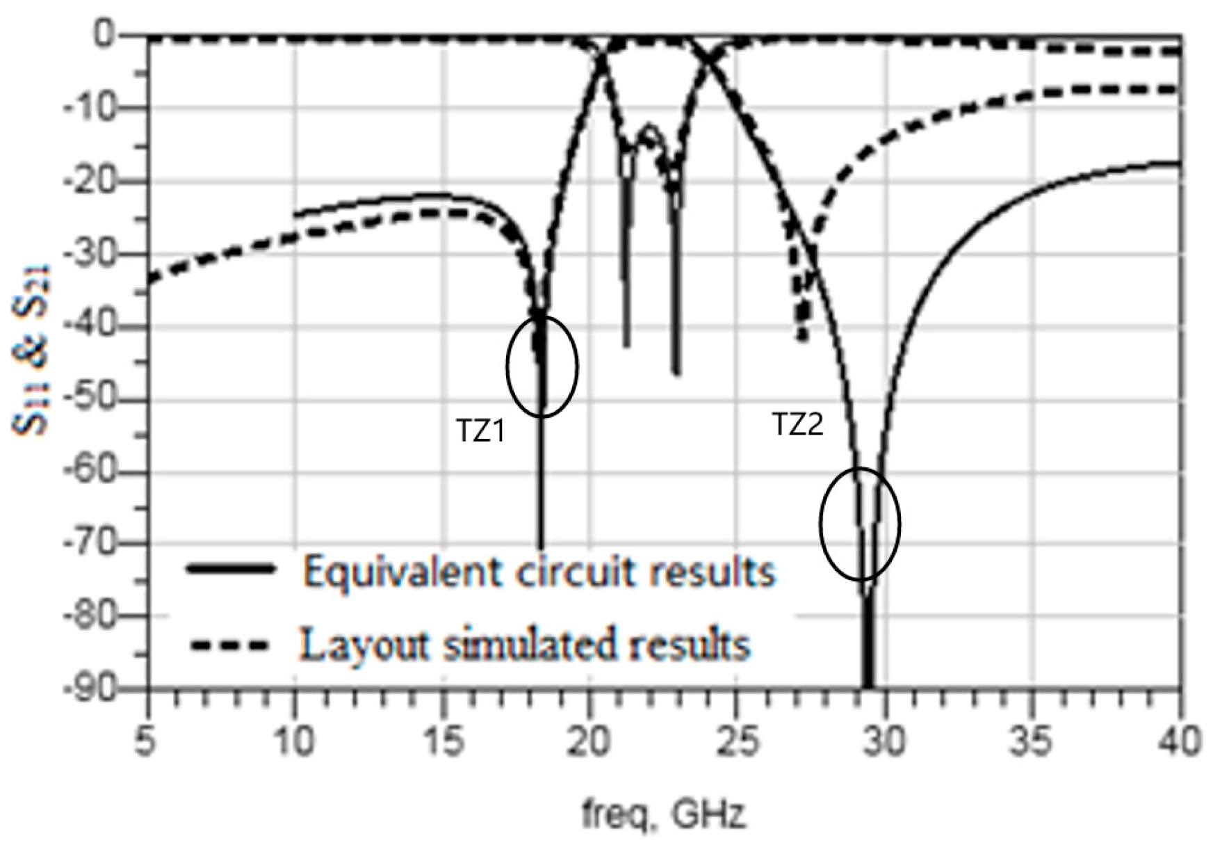
2. Equivalent Circuit Model Analysis

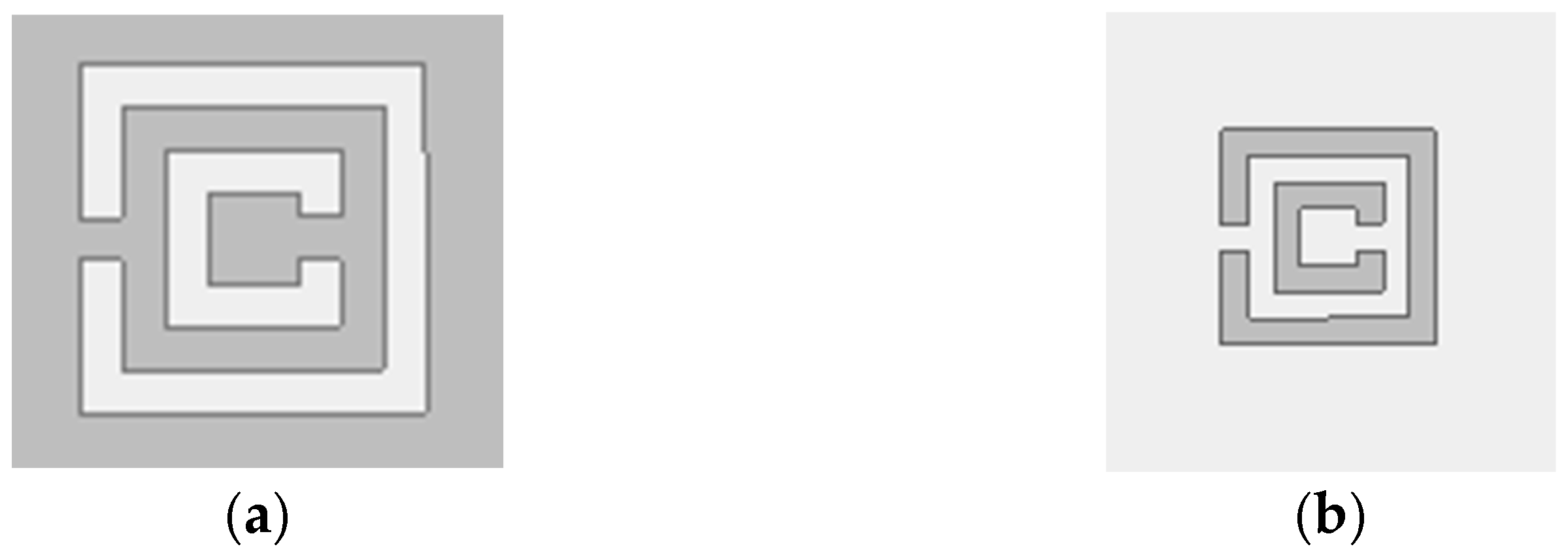
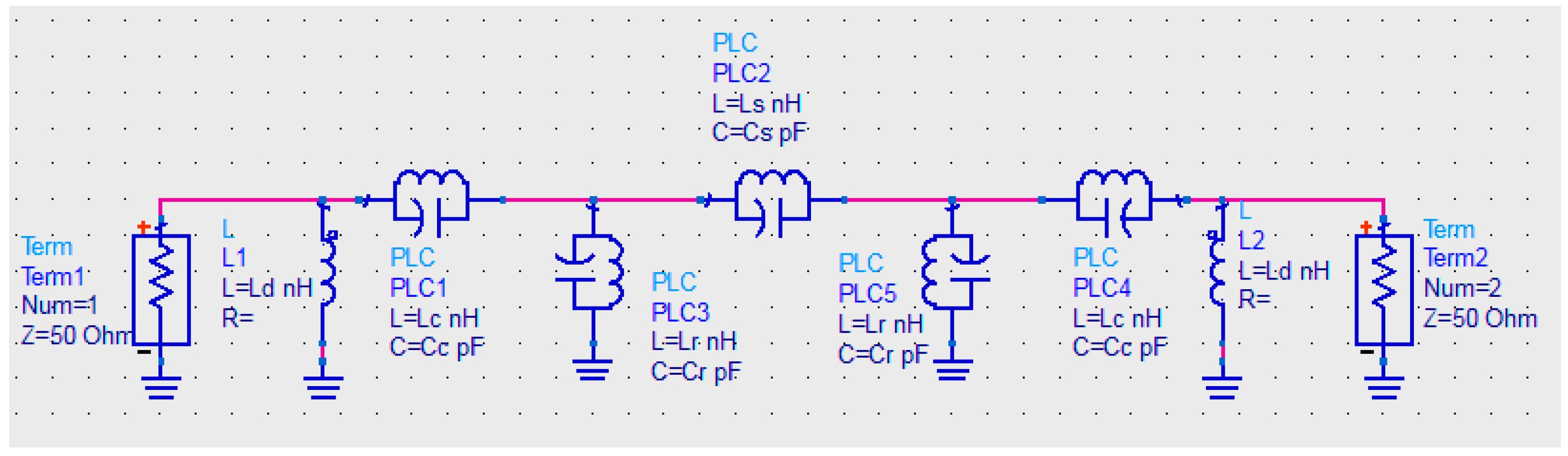
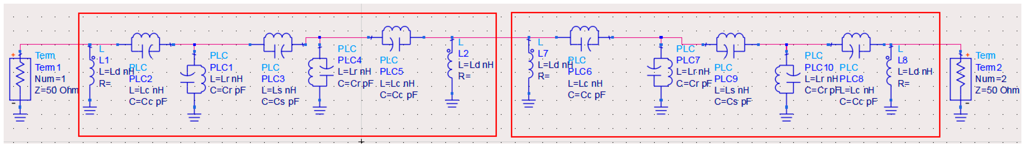
2.1. Lumped Model of the Proposed Filter Unit

Figure 3 shows the equivalent lumped circuit model of the SIW resonator loaded with CSRRs [32]. In this model, the SIW transmission line is represented by the equivalent parallel inductance Ld, which simulates the high-pass effect of a waveguide. The CSRR resonator is represented by the equivalent components Lr and Cr, which form the resonant unit. The inductance, Lc, is mainly determined by the small metal piece connecting the SIW and the inner metal ring of the CSRR, while the capacitance, Cc, is mainly determined by the coupling strength between the SIW and the inner metal ring. The parameters Ls and Cs represent the electrical and magnetic couplings between the CSRR resonators, respectively. When Ls and Cs form resonance, a transmission zero will occur below the passband, and the frequency of this transmission zero, denoted as fZ1, satisfies Equation (1).
f Z 1 = 1 2 π L s C s
Similarly, when Lc and Cc form resonance, a transmission zero will occur above the passband, and the frequency of this transmission zero, denoted as fZ2, satisfies Equation (2).
f Z 2 = 1 2 π L c C c
Theoretically, since there are two transmission zeros caused by resonances, the out-of-band suppression should be higher. However, due to the proximity of the upper passband to the theoretical passband of the substrate-integrated waveguide (SIW), the situation becomes more complicated. In the layout simulation results using Ansys HFSS, the attenuation values outside the upper passband do not exactly match the lumped parameter equivalent model. Nevertheless, the overall trend still holds, as shown in Figure 4. Increasing Ld enhances the external coupling, causing the in-band poles to approach each other and the out-of-band suppression level to deteriorate. Increasing Lc or Cc shifts the frequency of transmission zero TZ2 downwards, slightly lowers the passband frequency, weakens the external coupling, and separates the in-band poles, leading to worsened standing waves. Increasing Ls or Cs shifts the frequency of transmission zero, TZ1, downwards, keeps the high-frequency pole frequency inside the passband unchanged, and lowers the low-frequency pole, causing standing waves to worsen. Additionally, the out-of-band suppression at higher frequencies is hardly affected. Increasing Lr or Cr lowers the in-band resonant frequency, brings the in-band poles closer to each other, improves the in-band standing waves, deteriorates the low-frequency out-of-band suppression, and keeps the position of the out-of-band transmission zero unchanged.
There is a relatively clear correspondence between the various physical dimensions of layouts and lumped capacitors, inductors. In other words, the topology of the approximate equivalent lumped circuit is well defined, as shown in Figure 3. By varying the value of a single physical dimension parameter through parameter sweeping in HFSS, we observed that adjusting the values of corresponding lumped elements can maintain a match between electromagnetic simulation and lumped circuit simulation response curves. This allows us to infer the correctness of the lumped circuit topology. However, the complex formula that directly correlates physical dimensions with lumped parameters is difficult to express precisely using explicit equations. Despite referencing numerous related studies, none of them provide an explicit corresponding formula. As for the values of the components in the equivalent circuit, after deducing the topology of the equivalent circuit, we obtained these parameters through fitting the simulation result curves.

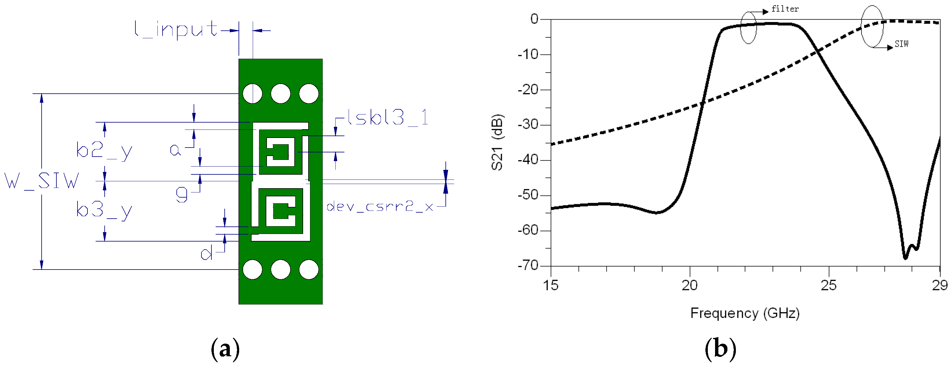
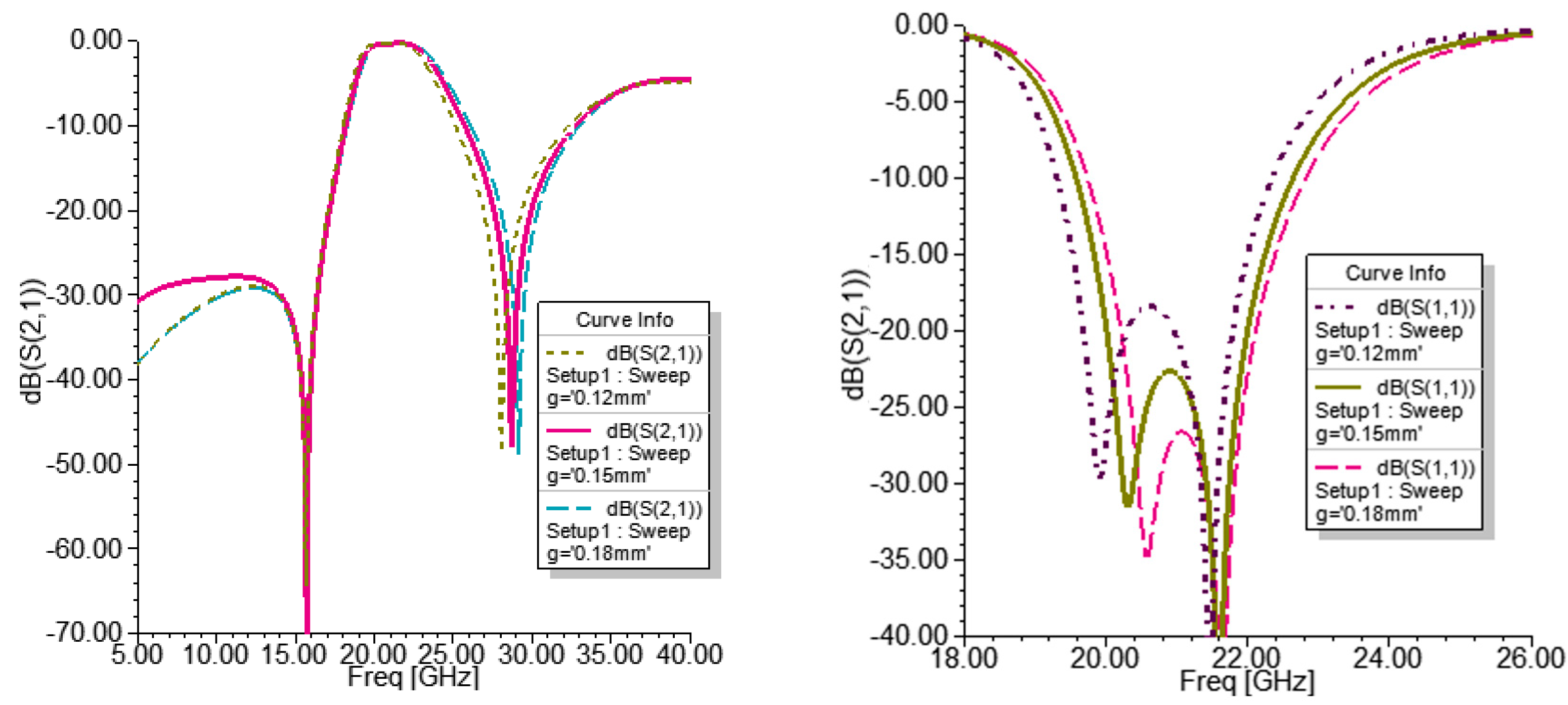
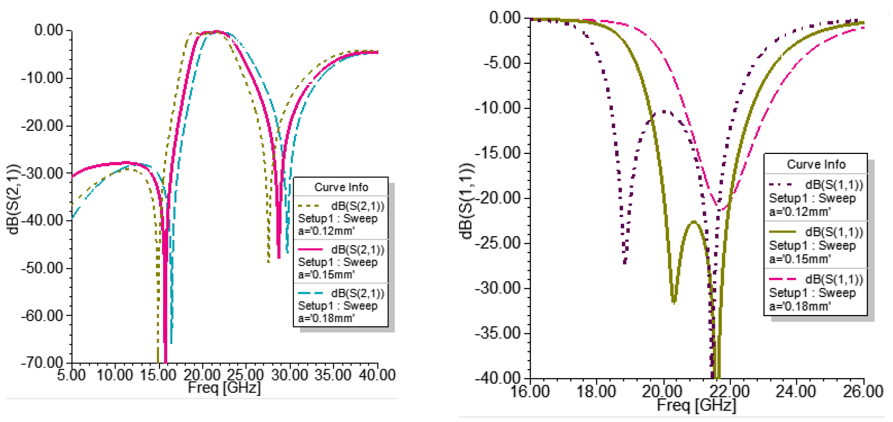
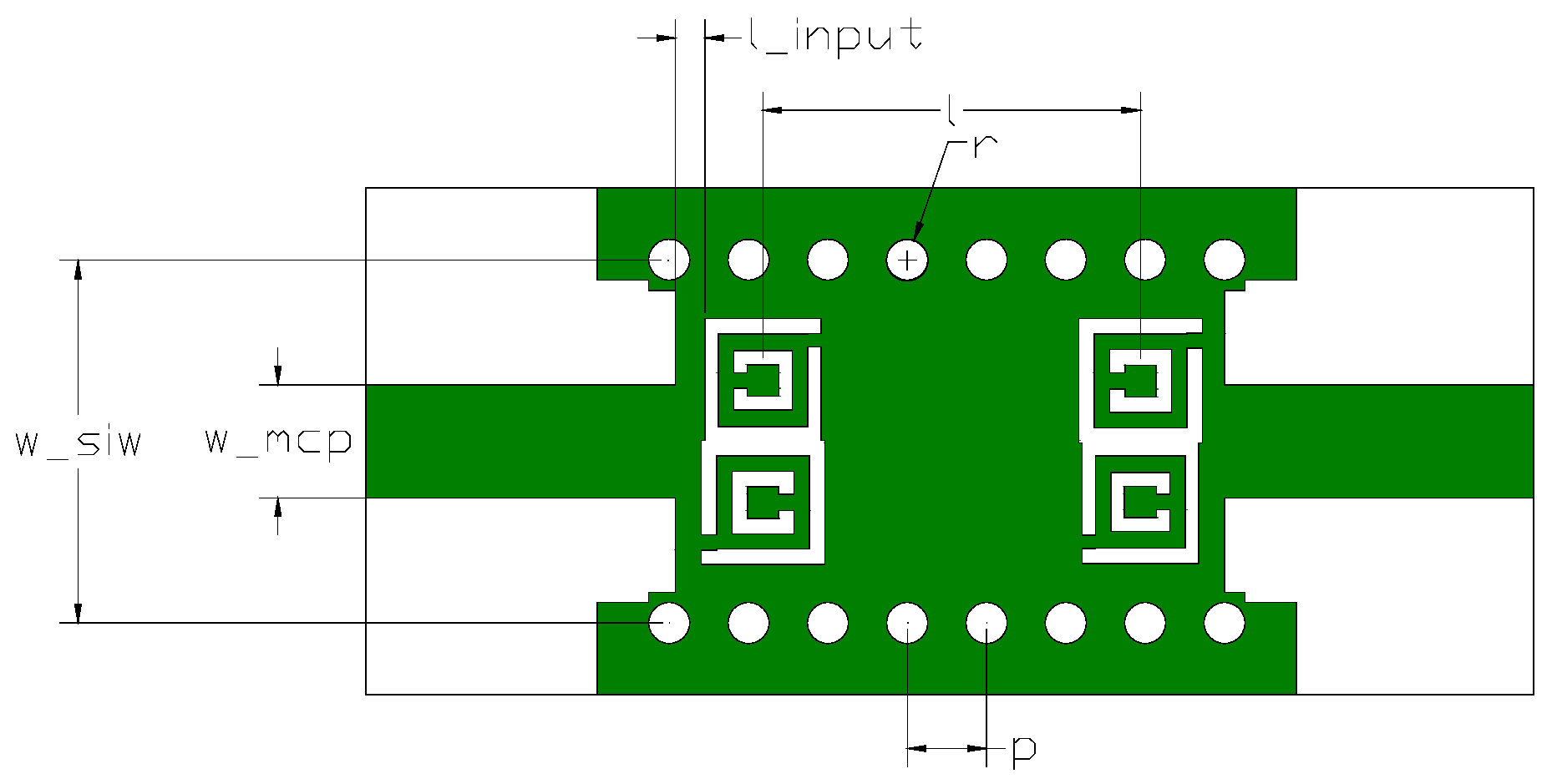
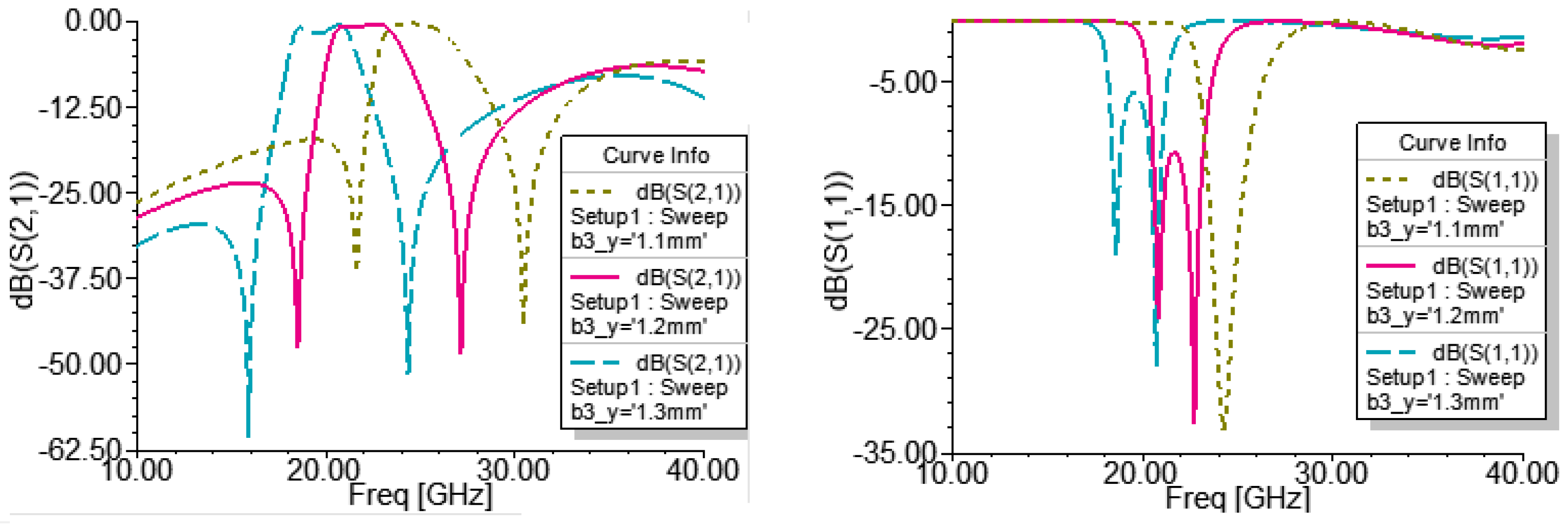
2.2. Relationship between Lumped Model Parameters and Layout Parameters

Next, the correspondence between the parameters in Figure 2a and the lumped parameter equivalent model was studied.
When the width of the SIW transmission line (w_siw) changes, it does not alter the coupling value. However, increasing Ld (which occurs when the SIW is wider, resulting in a larger inductance) enhances the external coupling, deteriorates the out-of-band suppression level, improves the in-band standing waves, and brings the in-band poles closer to each other, as shown in Figure 5.
The width of the input edge (l_input) affects both the external coupling and the internal coupling between CSRRs. A larger edge weakens the external coupling, and as Ld decreases, the internal coupling between CSRRs decreases with the increase in edge width. This leads to an upward shift in the frequency of transmission zero, TZ1, as shown in Figure 6.
The variation in the side length of the CSRR resonator (b3_y) affects both the internal and external couplings. When considering external coupling, if the size of the CSRR resonator is increased, it is like making the SIW narrower. This leads to a smaller Ld, as illustrated in Figure 7. When the difference in the side length of the CSRR resonator and the SIW is kept constant, the out-of-band suppression level remains similar, as shown in Figure 8. Additionally, the size of the resonator affects the coupling between the SIW cavity and the resonator and the coupling within the resonator itself. When the CSRR size increases, both Cc and Cs decrease, causing both transmission zeros and the resonator frequency to shift upwards. Overall, this is similar to a frequency band shift; however, due to the decrease in Cc and Cs leading to pole proximity, the poles may merge when the resonator size increases to a certain extent.
When the width of the coupling slot line between the two CSRR resonators (dev_csrr2_x) is varied, as shown in Figure 9, the internal coupling weakens with a positive value of dev_csrr2_x, indicating that the CSRR resonators are placed close together, while a negative value means that the two resonators have overlapping sections. The most significant effect is on the internal coupling, with Cs increasing and the frequency of transmission zero TZ2 shifting downwards. Moreover, Cc is slightly affected, with an increase leading to a slight upward shift in the transmission zero, TZ1. Furthermore, the CSRR resonator is also slightly affected, leading to a slight downward shift in the center frequency of the passband, and the two poles move closer to each other, improving the in-band standing waves.
When the position of the small metal piece connecting the SIW and the inner metal ring (lsbl3_1) is changed, as shown in Figure 10, the internal coupling field is significantly affected. From the perspective of field distribution, the magnetic field is strongest and the electric field is weakest at the metal connection point. Therefore, changing the position of the connection point will result in significant variations in the coupling field distribution between the two CSRR resonators. When the connection point is closer to the feeding microstrip line, the coupling field at that position becomes stronger, and as a result, Ls increases, the frequency of transmission zero TZ2 shifts downwards, and the passband frequency slightly decreases, leading to separated poles.
The traditional design corresponds to the result when lsbl3_1 = 0. In our design, introducing the design variable lsbl3_1 makes it easier to achieve a large or small bandwidth by adjusting the coupling strength between the two CSRR structures. In the traditional design, the key parameter for controlling the coupling strength between the two CSRR structures is the distance between them (dev_csrr2_x). This implies that the maximum bandwidth is constrained by the minimum distance, and achieving a small bandwidth requires a larger distance, resulting in increased spatial requirements. For this design, we chose dev_csrr2_x = 0.
The size of the connection metal (d) and the size of the metal strip inside the resonator (g) affect the inductance, Lc. Similar to the microstrip transmission line, a larger width means lower characteristic impedance and smaller unit series inductance based on the theory of transmission line. The larger the metal size, the smaller the inductance, Lc, as shown in Figure 11 and Figure 12. The effect is the same: improved in-band low-frequency, out-of-band suppression, an upward shift of the transmission zero TZ2 frequency, and a slight upward shift of the passband frequency. The external coupling increases, the in-band poles approach each other, and the standing waves improve, while the out-of-band suppression shows no fixed pattern.
The width of the slot (a) between the SIW and CSRR affects the capacitance, Cc. A wider slot results in a smaller capacitance, Cc, and the variation trend is the same as that when Lc decreases, as shown in Figure 13.
With the above design foundation, the desired target S-parameter curve can be obtained using the lumped parameter model. Then, by changing the dimensions of the layout that affect the relevant lumped components, simulations can be performed to achieve the desired S parameters. When multiple stages are cascaded, the lumped parameter model can be cascaded as well. Figure 14 shows the cascade of two stages, and the schematic simulated results of a fourth-order K-band filter are illustrated in Figure 15 with the values of capacitors and inductors in Figure 4. However, due to the lack of accuracy of the model at the connection point, the final dimensions may need further optimization. Additionally, it is worth noting that the equivalent circuit model provided here for lumped parameters cannot accurately fit the response of the high-frequency parasitic passband. As a result, the determination of the high-frequency parasitic passband needs to be based on prior calculations of the substrate-integrated waveguide’s cutoff frequency. Nonetheless, despite this limitation, the lumped parameter model still holds significant guiding significance for the passband design considered herein. The relationship between the layout and the lumped circuits model can provide some guidance on the trend.
Regarding the design of transmission zeros, we can also draw insights from the cascaded lumped parameter equivalent circuit. Based on the discussion of single-stage equivalent circuits, a single stage of the CSRR group can generate two transmission zeros. The low-frequency transmission zero is determined by the resonance of Ls and Cs, denoted as fZL1, while the high-frequency transmission zero is determined by the resonance of Lc and Cc, denoted as fZH1. Therefore, theoretically, a two-stage circuit can generate twice the number of transmission zeros, namely fZL1, fZL2, fZH1, and fZH2. In the context of the topology shown in Figure 14, the transmission zeros generated by the first-stage cell and the second-stage cell would completely coincide, namely fZL1 = fZL2 and fZH1 = fZH2. However, by slightly adjusting the values of design parameters, such as introducing differences in Cc (Lc) and Cs (Ls) between the first stage and the second stage, resonant frequencies along the series’ main path can be made distinct. This allows the overlapping transmission zeros to separate into four distinct transmission zeros.
It is important to note that achieving a complete separation of the overlapping transmission zeros is not always necessary, as the out-of-band suppression achieved with slightly separated transmission zeros is comparable. Hence, during the design process, it might not be imperative to entirely separate the transmission zeros generated by the first stage and the second stage.

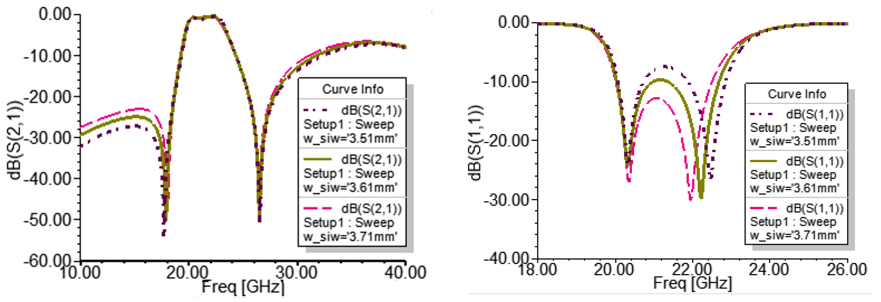
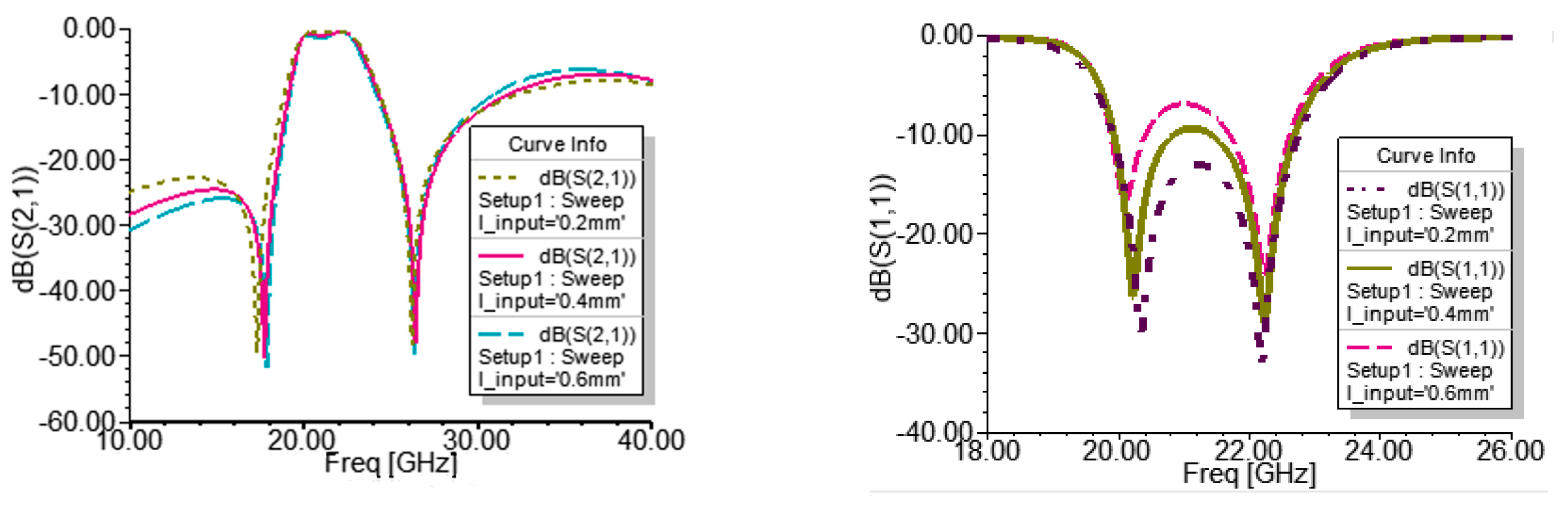
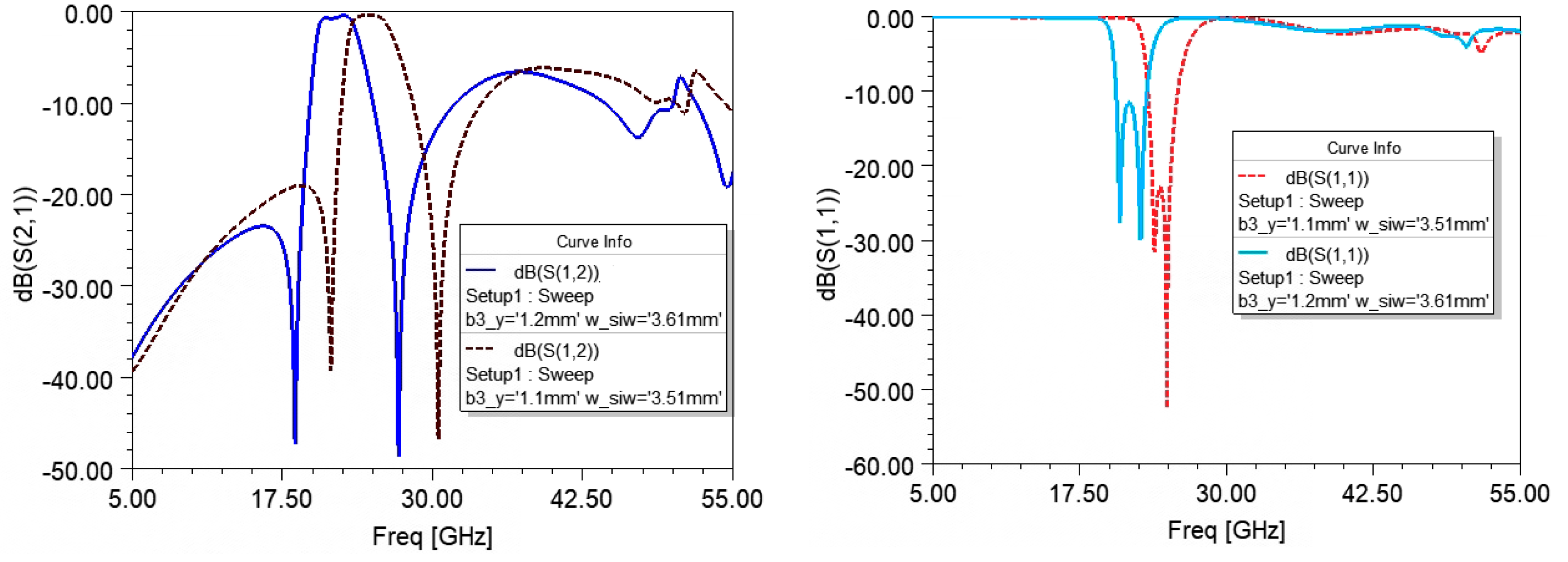
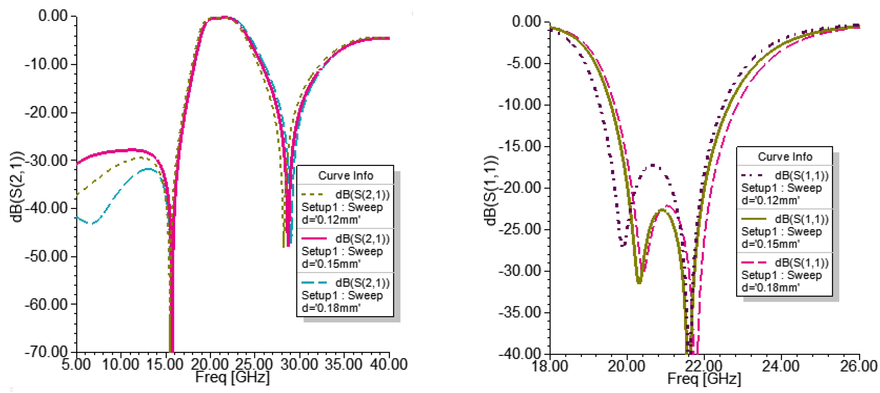
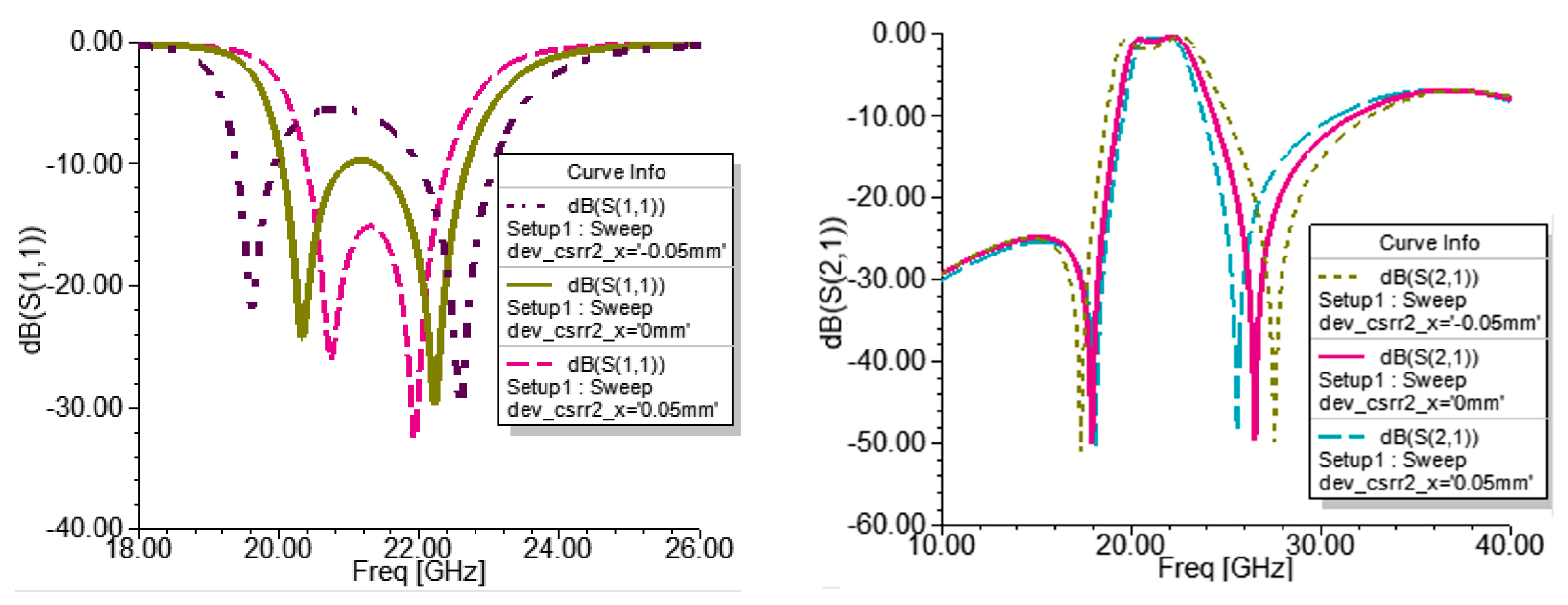
3. A K-Band Filter Design

The K-band filter design applies an RT/Duroid 4350 substrate with a thickness of 0.508 mm and a relative dielectric constant of 3.48. The metal via holes have a diameter of 0.4 mm and are spaced 0.75 mm apart. Figure 14 shows the layout of the filter, with a 50-ohm microstrip line used for direct feeding. The core structure of the filter is composed of surface-etched CSRR structures on the SIW. To enhance the coupling between adjacent CSRRs, the middle metal strip is also etched away, which compresses the TE10 field distribution and achieves stronger coupling.
The dimensions other than those of the CSRR resonators are annotated in Figure 16, and the dimensions of the internal CSRR structure are shown in Figure 2a. The entire design process can be divided into two steps: First, based on the predetermined design requirements of the filter, the initial value of the SIW width (w_siw) is determined to ensure that the SIW cutoff frequency is higher than the passband frequency of the filter. Then, the dimensions of the two CSRRs are adjusted. There are only two dimensions that have a significant impact on the resonant frequency: the size of the ring itself (b2_y, b3_y) and the size (d) and position (lsbl3_1) of the opening in the ring. Keeping other dimensions fixed, the resonant frequency will decrease with an increase in the size of the ring itself, and it will increase with an increase in the size of the opening. The bandwidth can be adjusted by adjusting the distance (dev_csrr2_x) between the edges of adjacent resonators. The closer the distance, the stronger the coupling and the wider the bandwidth. The coupling strength can also be adjusted by fine-tuning the position of the outer ring opening (lsbl3_1). Using the three-dimensional commercial simulation software Ansys HFSS, the final dimensions of the CSRRs can be obtained after optimization. Assuming that the filter operates in the range of 21.2 GHz to 23.9 GHz, the dimensions obtained after simulation optimization are listed in Table 1, and Figure 17 shows a photo of the filter. The core size of the filter is about 5.3 mm × 4 mm. Two 2.92 mm (K) connectors are soldered at the input and output port for measurement, supported by a test cavity.

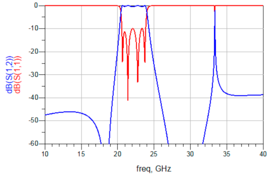
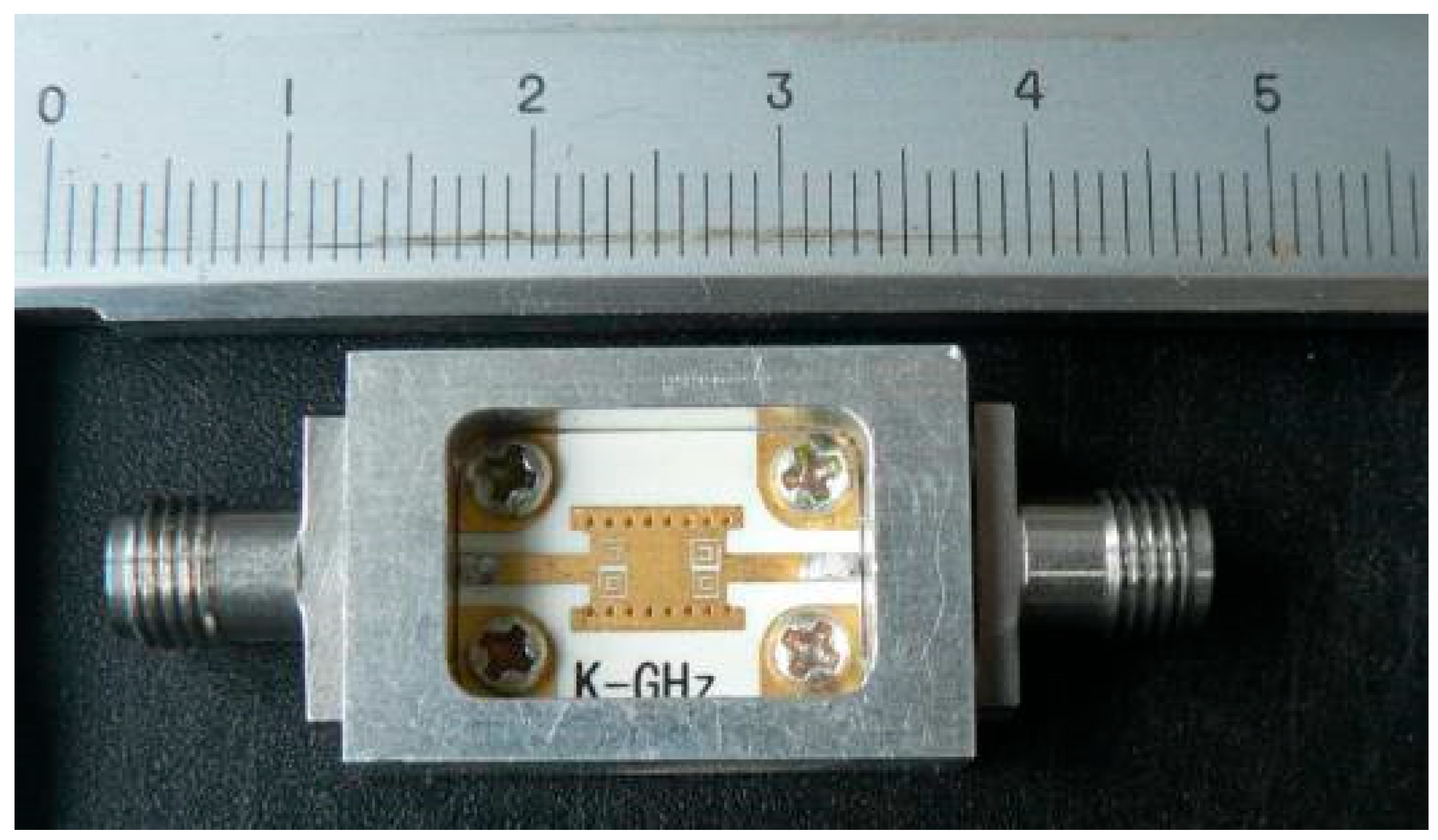
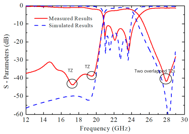
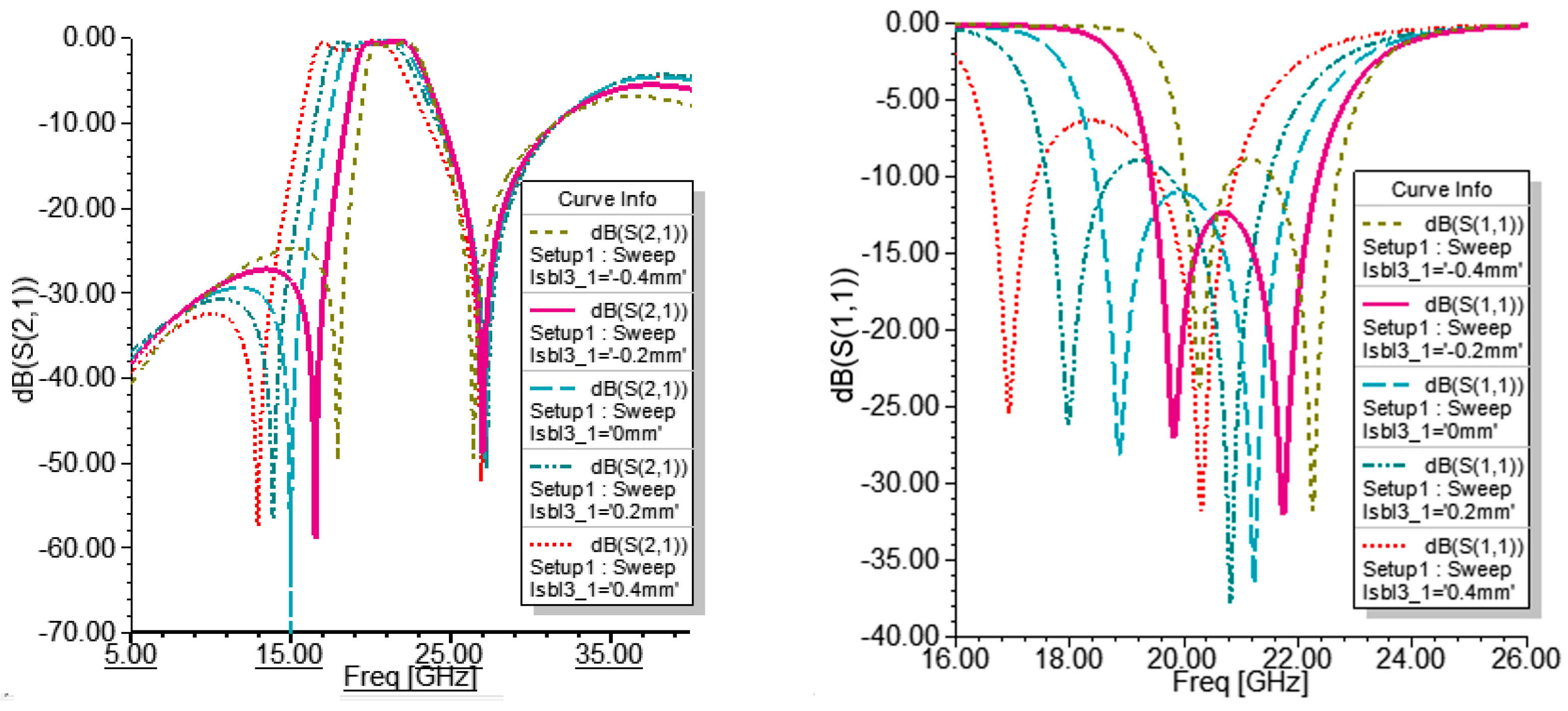
4. Measurement Results and Analysis

The SIW filter shown in Figure 17 was tested using an Agilent E8363B vector network analyzer. The test results and simulation results are both shown in Figure 18. The measured filter has a 1 dB bandwidth of 21.6 GHz to 24.3 GHz, with an insertion loss lower than 2 dB at the center frequency and a return loss better than 10 dB. The out-of-band suppression reaches below -30 dB. Two TZs lower than the passband and two overlapping TZs above the passband are realized to improve the skirt selectivity. The two overlapping TZs can be separated or overlapped by slightly adjusting the design parameters from the equivalent circuit model simulation results or HFSS simulation results. Compared to the simulation results, the measured results show an obvious discrepancy at the higher end of the passband, which is mainly caused by processing errors in the etching slot. The low-frequency out-of-band suppression level is far from that seen in the simulation. After verification in HFSS, we can deduce this is due to the influence of the testing cavity, and better out-of-band suppression can be achieved by improving the cavity design.
For simplicity of design, we opted not to include screws, and thus conducted simulations with smaller metal cavities, yielding favorable results. However, we observed that large cavities generate parasitic resonances, which can impact the lower stopband rejection of the filter after measurement. While simulating a larger cavity might yield results closer to the testing outcomes, it fails to reveal the intended performance of the design. In practical usage, we can still mitigate the impact of cavity-induced parasitic resonances on low-frequency stopband rejection by using metal shims or blocks to raise the screws and achieve smaller cavities. Comparisons between our design and the state of the art are presented in Table 2. The results demonstrate that our design achieves a relatively compact size and an adequate number of transmission zeros, contributing to enhanced out-of-band suppression, particularly at lower out-of-band frequencies.

5. Conclusions

In this study, we have presented a good approach to achieving miniaturization and enhanced performance in substrate-integrated waveguide (SIW) filters by leveraging the unique electromagnetic properties of improved Complementary Split-Ring Resonators (CSRRs). These resonant structures have gained significant attention for their capabilities in realizing negative permeability and negative permittivity, making them promising candidates for advanced microwave devices. We have designed and analyzed a compact SIW filter loaded with these improved CSRRs, capitalizing on their ease of integration onto the SIW surface.
Our investigation began with a comprehensive overview of the intriguing electromagnetic characteristics exhibited by CSRRs. These resonators, initially introduced by Falcone and his team, have played a pivotal role in advancing the field of metamaterials. Their ability to manifest negative permeability and negative permittivity has opened up new possibilities for the design and development of unconventional microwave components. We embarked on a historical journey, tracing the roots of these resonant structures back to the groundbreaking work of J.B. Pendry. We delved deep into the intricacies of CSRRs, unveiling their electric dipole nature when subjected to axial electric field excitation. This profound comprehension of the fundamental principles governing CSRRs laid a strong foundation for our research endeavors.
By merging two CSRRs and modifying the opening directions of the outer ring, we achieved adjustable coupling types (electric or magnetic coupling) and strengths, providing greater flexibility in filter design compared to traditional CSRR structures with a central opening. The comprehensive study and experimental investigation of the combined application of SIW and CSRRs above 20 GHz have effectively filled the research gap in this frequency range.
The analysis of the SIW transmission line loaded with CSRR resonators was conducted using the lumped parameter model, and the correspondence between the layout parameters and the lumped components in the equivalent model was analyzed. Subsequently, a K-band bandpass filter was successfully designed and implemented using the described CSRR-loaded SIW filter. The measurement results demonstrate that the filter exhibits excellent passband characteristics, and the measured results are in good agreement with the simulation results. This research paves the way for further advancements in SIW filter design and implementation, leveraging the advantages of CSRRs in achieving miniaturization and enhanced filter performance in the higher frequency ranges.

Funding

This research was funded by [National Natural Science Foundation of China] grant number [62101193].

Data Availability Statement

No new data were created or analyzed in this study. Data sharing is not applicable to this article.

Conflicts of Interest

The authors declare no conflict of interest.

References

  1. Pendry, J.B.; Holden, A.J.; Robbins, D.J.; Stewart, W.J. Magnetism from conductors and enhanced nonlinear phenomena. IEEE Trans. Microw. Theory Tech. 1999, 47, 2075–2084. [Google Scholar] [CrossRef]
  2. Falcone, F.; Lopetegi, T.; Baena, J.D.; Marques, R.; Martin, F.; Sorolla, M. Effective negative-epsilon stopband microstrip lines based on complementary split ring resonators. IEEE Microw. Wirel. Compon. Lett. 2004, 14, 280–282. [Google Scholar] [CrossRef]
  3. Saadat-Safa, M.; Nayyeri, V.; Khanjarian, M.; Soleimani, M.; Ramahi, O.M. A CSRR-Based Sensor for Full Characterization of Magneto-Dielectric Materials. IEEE Trans. Microw. Theory Tech. 2019, 67, 806–814. [Google Scholar] [CrossRef]
  4. Wu, W.-J.; Zhao, W.-S.; Wang, D.-W.; Yuan, B.; Wang, G. A Temperature-Compensated Differential Microstrip Sensor for Microfluidic Applications. IEEE Sens. J. 2021, 21, 24075–24083. [Google Scholar] [CrossRef]
  5. Liu, Z.; Sharma, T.; Chappidi, C.R.; Venkatesh, S.; Yu, Y.; Sengupta, K. A 42–62 GHz Transformer-Based Broadband mm-Wave InP PA With Second-Harmonic Waveform Engineering and Enhanced Linearity. IEEE Trans. Microw. Theory Tech. 2021, 69, 756–773. [Google Scholar] [CrossRef]
  6. Hu, M.; Yu, Z.; Xu, J.; Lan, J.; Zhou, J.; Hong, W. Diverse SRRs Loaded Millimeter-Wave SIW Antipodal Linearly Tapered Slot Filtenna with Improved Stopband. IEEE Trans. Antennas Propag. 2021, 69, 8902–8907. [Google Scholar] [CrossRef]
  7. Khan, M.S.; Capobianco, A.-D.; Asif, S.M.; Anagnostou, D.E.; Shubair, R.M.; Braaten, B.D. A Compact CSRR-Enabled UWB Diversity Antenna. IEEE Antennas Wirel. Propag. Lett. 2017, 16, 808–812. [Google Scholar] [CrossRef]
  8. Ding, Y.; Lee, C.-S.; Li, Y.; Wang, Z.-Q.; Li, G.-F. An Angular Displacement Sensor-Based Active Feedback Open Complementary Split-Ring Resonator. IEEE Microw. Wirel. Compon. Lett. 2021, 31, 1079–1082. [Google Scholar] [CrossRef]
  9. Liu, Z.; Sengupta, K. A 44–64-GHz mmWave Broadband Linear Doherty PA in Silicon with Quadrature Hybrid Combiner and Non-Foster Impedance Tuner. IEEE J. Solid-State Circuits 2022, 57, 2320–2335. [Google Scholar] [CrossRef]
  10. Feng, W.; Shi, Y.; Zhou, X.Y.; Shen, X.; Che, W. A Bandpass Push–Pull High Power Amplifier Based on SIW Filtering Balun Power Divider. IEEE Trans. Plasma Sci. 2019, 47, 4281–4286. [Google Scholar] [CrossRef]
  11. Marques, R.; Martel, J.; Mesa, F.; Medina, F. Left-handed-media simulation and transmission of EM waves in subwavelength split ring resonator-loaded metallic waveguides. Phys. Rev. Lett. 2002, 89, 183901–183904. [Google Scholar] [CrossRef] [PubMed]
  12. Baena, J.N.; Marques, R.; Martel, J.; Medina, F. Experimental results on metamaterial simulation using SRR-loaded waveguides. In Proceedings of the IEEE Antennas and Propagation Society International Symposium. Digest. Held in conjunction with: USNC/CNC/URSI North American Radio Sci. Meeting (Cat. No.03CH37450), Columbus, OH, USA, 22–27 June 2003; Volume 1, pp. 106–109. [Google Scholar]
  13. Hrabar, S.; Bartolic, J.; Sipus, Z. Waveguide miniaturization using uniaxial negative permeability metamaterial. IEEE Trans. Antennas Propag. 2005, 53, 110–119. [Google Scholar] [CrossRef]
  14. Esteban, J.; Penalosa, C.C.; Page, J.E.; Martin-Guerrero, T.M.; Marquez-Segura, E. Simulation of negative permittivity and negative permeability by means of evanescent waveguide modes-theory and experiment. IEEE Trans. Microw. Theory Tech. 2005, 53, 1506–1514. [Google Scholar] [CrossRef]
  15. Lubkowski, G.; Damm, C.; Bandlow, B.; Schuhmann, R.; Schüßler, M.; Weiland, T. Broadband transmission below the cutoff frequency of a waveguide loaded with resonant scatterer arrays. IET Microw. Antennas Propag. 2007, 1, 165–169. [Google Scholar] [CrossRef]
  16. Bage, A.; Das, S. Stopband Performance Improvement of CSRR-Loaded Waveguide Bandpass Filters Using Asymmetric Slot Structures. IEEE Microw. Wirel. Compon. Lett. 2017, 27, 697–699. [Google Scholar] [CrossRef]
  17. Zhu, H.-R.; Sun, Y.-F.; Wu, X.-L. A Compact Tapered EBG Structure with Sharp Selectivity and Wide Stopband by Using CSRR. IEEE Microw. Wirel. Compon. Lett. 2018, 28, 771–773. [Google Scholar] [CrossRef]
  18. Jiang, D.; Liu, Y.; Li, X.; Wang, G.; Zheng, Z. Tunable Microwave Bandpass Filters with Complementary Split Ring Resonator and Liquid Crystal Materials. IEEE Access 2019, 7, 126265–126272. [Google Scholar] [CrossRef]
  19. Jha, A.K.; Lamecki, A.; Gómez-García, R.; Mrozowski, M. Extending the Frequency Limit of Microstrip-Coupled CSRR Using Asymmetry. IEEE Trans. Microw. Theory Tech. 2021, 69, 3759–3769. [Google Scholar] [CrossRef]
  20. Zhang, S.; Rao, J.-Y.; Hong, J.-S.; Liu, F.-L. A Novel Dual-Band Controllable Bandpass Filter Based on Fan-Shaped Substrate Integrated Waveguide. IEEE Microw. Wirel. Compon. Lett. 2018, 28, 308–310. [Google Scholar] [CrossRef]
  21. Zeng, X.; Bi, X.; Cao, Z.; Wan, R.; Xu, Q. High Selectivity Dual-Wideband Balun Filter Utilizing a Multimode T-line Loaded Middle-Shorted CSRR. IEEE Trans. Circuits Syst. II Express Briefs 2020, 67, 2447–2451. [Google Scholar] [CrossRef]
  22. Zhang, H.; Kang, W.; Wu, W. Miniaturized Dual-Band Differential Filter Based on CSRR-Loaded Dual-Mode SIW Cavity. IEEE Microw. Wirel. Compon. Lett. 2018, 28, 897–899. [Google Scholar] [CrossRef]
  23. Ji, Q.; Yang, H.; Wang, T.; Fang, X.; Jiang, T.; Xu, Q.; Cao, Z. CSRR DGS-Based Bandpass Negative Group Delay Circuit Design. IEEE Access 2023, 11, 20309–20318. [Google Scholar] [CrossRef]
  24. Zhang, X.C.; Yu, Z.Y.; Xu, J. Novel band-pass substrate integrated waveguide (SIW) filter based on complementary split ring resonators (CSRRs). Prog. Electromagn. Res. 2007, 72, 39–46. [Google Scholar] [CrossRef]
  25. Fu, W.; Li, Z.; Liu, P.; Cheng, J.; Qiu, X. Modeling and analysis of novel CSRRs-loaded dual-band bandpass SIW filters. IEEE Trans. Circuits Syst. II Express Briefs 2021, 68, 2352–2356. [Google Scholar] [CrossRef]
  26. Dong, Y.D.; Yang, T.; Itoh, T. Substrate integrated waveguide loaded by complementary split-ring resonators and its applications to miniaturized waveguide filters. IEEE Trans. Microw. Theory Tech. 2009, 57, 2211–2223. [Google Scholar] [CrossRef]
  27. Shi, L.F.; Sun, C.Y.; Chen, S.; Liu, G.X.; Shi, Y.F. Dual-band substrate integrated waveguide bandpass filter based on CSRRs and multimode resonator. Int. J. RF Microw. Comput. Aid. Eng. 2018, 28, e21412. [Google Scholar] [CrossRef]
  28. Zhang, H.; Wei, K.; Wen, W. Dual-band substrate integrated waveguide bandpass filter utilising complementary split-ring resonators. Electron. Lett. 2018, 54, 85–87. [Google Scholar] [CrossRef]
  29. Chu, P.; Hong, W.; Zheng, K.L.; Yang, W.W.; Xu, F.; Wu, K. Balanced hybrid SIW–CPW bandpass filter. Electron. Lett. 2017, 53, 1653–1655. [Google Scholar] [CrossRef]
  30. Achraou, S.; Haddi, S.B.; Zakriti, A.; El Ouahabi, M.; Farkhsi, A. A Compact SIW Bandpass Filter with Double slit Complementary Split Ring Resonator. In Proceedings of the 2020 International Symposium on Advanced Electrical and Communication Technologies (ISAECT), Marrakech, Morocco, 25–27 November 2020; pp. 1–4. [Google Scholar]
  31. Mehdi, D.; Keltouma, N.; Mohammed, F.; Mohammed, K. Comparison on the Substrat Integerated Wave Guide Filter Based on Complementary Split Ring Resonators (CSRRs). Int. J. Comput. Sci. Telecommun. 2015, 6, 10–16. [Google Scholar]
  32. Rogla, L.J.; Carbonell, J.; Boria, V.E. Study of equivalent circuits for open-ring and split-ring resonators in coplanar waveguide technology. IET Microw. Antennas Propag. 2007, 1, 170–176. [Google Scholar] [CrossRef]
Figure 1. (a) Split-Ring Resonator (SRR); (b) Complementary Split-Ring Resonator (CSRR) (the white parts represent metal, and the gray parts represent the substrate).
Electronics 12 03789 g001
Figure 2. (a) The proposed filter unit: SIW resonator loaded with improved CSRRs; (b) comparison between an SIW filter with loaded CSRR and an SIW filter without CSRR.
Electronics 12 03789 g002
Figure 3. Equivalent circuit of the proposed filter unit in Figure 2a.
Electronics 12 03789 g003
Figure 4. Comparison of layout simulation and lumped parameter simulation results. Ld = 0.592, Lc = 0.151, Lr = 0.24, Ls = 0.415, Cc = 0.196, Cr = 0.266, and Cs = 0.18.
Electronics 12 03789 g004
Figure 5. Influence of the SIW transmission line width (w_siw) on S parameters.
Electronics 12 03789 g005
Figure 6. Influence of the input edge width (l_input) on S parameters.
Electronics 12 03789 g006
Figure 7. Influence of the outer perimeter side length of the CSRR resonator (b3_y) on S parameters.
Electronics 12 03789 g007
Figure 8. S-parameter variation when the distance between w_siw and b3_y is kept constant.
Electronics 12 03789 g008
Figure 9. Influence of dev_csrr2_x on S parameters.
Electronics 12 03789 g009
Figure 10. Influence of lsbl3_1 on S parameters.
Electronics 12 03789 g010
Figure 11. Influence of d on S parameters.
Electronics 12 03789 g011
Figure 12. Influence of g on S parameters.
Electronics 12 03789 g012
Figure 13. Influence of a on S parameters.
Electronics 12 03789 g013
Figure 14. Cascade of two stages of the structures in Figure 3.
Electronics 12 03789 g014
Figure 15. Simulated S−parameters results of the circuit in Figure 14.
Electronics 12 03789 g015
Figure 16. Layout of the SIW filter with improved CSRRs.
Electronics 12 03789 g016
Figure 17. SIW filter with improved CSRR physical diagram.
Electronics 12 03789 g017
Figure 18. Simulated and measured results of the fabricated filter.
Electronics 12 03789 g018
Table 1. Filter dimensions (mm).
b2_yb3_ygdalrpw_siww_mcpl_inputdev_csrr2_x
1.211.240.150.150.152.50.20.753.621.10.250
Table 2. Comparison with other SIW filters.
Ref.f0 (GHz)OrderFBW (%)IL at f0
(dB)
TZs (L/M/H)Main Size
(λg × λg)
[22]6.22/8.242/206.22/8.240.86/1.320/2/10.86 × 0.41
[25]6/122/318.33/29.170.79/1.390/2/20.92 × 0.534
[27]9.8/13.52/211.2/9.81.8/1.51/1/11.22 × 1.22
[28]7.89/8.892/23.42/3.941.5/1.91/2/10.87 × 0.85
[29]5.56121.70/0/00.78 × 0.39
[30]8.32180.4 (Sim)0/0/00.91 × 0.354
[31]8.35319.270.85 (Sim)0/0/31.08 × 0.626
This work22.95411.761.962/0/20.756 × 0.57
Notes: In the table, “L” represents the count of transmission zeros at the low-frequency stopband, and “H” represents the count of transmission zeros at the high-frequency stopband. In the case of dual-band filters, “M” indicates the count of transmission zeros between the two passbands.
Disclaimer/Publisher’s Note: The statements, opinions and data contained in all publications are solely those of the individual author(s) and contributor(s) and not of MDPI and/or the editor(s). MDPI and/or the editor(s) disclaim responsibility for any injury to people or property resulting from any ideas, methods, instructions or products referred to in the content.

