Abstract
In this paper, a new realization of electronically tunable voltage output second-order low-pass (LP) and band-pass (BP) filter is presented. The circuit has a multiple-input single-output structure, and LP and BP outputs are provided using the same structure. One electronically variable second-generation voltage conveyor (VCII), whose impedance at the Y port can be electronically varied using a control current (Icon), two capacitors, and one resistor are used. By changing the value of Icon, the impedance value at the Y port can be electronically varied; therefore, the value of ω0 can be tuned. This feature helps to reduce the number of passive components used. Interestingly, the LP and BP outputs are provided at the low-impedance Z port of the VCII, and there is no need for an extra voltage buffer for practical use. The circuit enjoys a simple realization consisting of only 24 MOS transistors. Simulation results using PSpice and 0.18 μm CMOS parameters are provided. The value of ω0 can be varied from 1.2 MHz to 1.7 MHz, while Icon varies from 0 to 50 µA, with a power consumption variation from 244 µW to 515 µW.
1. Introduction
Filter design represents a widespread and important topic, due to the interesting application in communication, measurement, instrumentation, control, and signal processing [1,2,3]. In recent years, current mode signal processing has been the focus of researchers in the design of various types of active filters. This is attributed to the numerous advantages offered by current mode signal processing, such as simple realization, high-frequency performance, low-voltage operation, etc. [4,5,6,7,8,9]. Importantly, current mode signal processing provides the opportunity of realizing electronically tunable filters, which are highly suitable for the requirements of full integration. These features have enabled various innovative current mode solutions in the realization of active filters [1,2,3,10,11,12,13,14,15,16,17,18,19].
A survey of the literature shows that considerable effort has been devoted to realizing filter topologies based on various current mode active building blocks (ABBs), such as current buffers (CBs) [1,3], second-generation current conveyors (CCIIs) [8,9,10,11], current differential transconductance amplifiers (CDTAs) [13], differential voltage current conveyors (DVCCs) [15,17], current differencing transconductance amplifiers (CCCTAs) [12,18], current feedback operational amplifiers (CFOAs) [19], current differencing buffered amplifiers (CDBAs) [20,21], fully differential CCIIs (FDCCIIs) [22], etc. However, the current mode active filters reported in [1,3,4,5,6,7,8,9,10,11,12,13,14,15,16,17,18,19,22] suffered from a common weakness of applications requiring voltage signals. In these circuits, the output signal was either in current form, making them unsuitable for applications requiring voltage signals, or in voltage form provided on a high impedance port, necessitating additional voltage buffers for practical use. In addition, the circuits reported in [1,3,10,11,15,17,18,19,20,21,22] were not electronically tunable. Moreover, the CB-based circuit reported in [3], which was able to realize all-pass and notch functions, required additional current followers (CFs) at the outputs for practical application. In the CCII-based circuit presented in [11], up to five active building blocks were used. The CCCTA- and CDTA-based filters presented in [12,13,18] were implemented using BJT technology. The filter reported in [16] suffered from circuit complications, because the FDCCII used as the active building block was realized using 60 MOS transistors, and thus required a high supply voltage of ±1.65 V. The topology of [17] employed three dual-output DVCC blocks with a total number of 84 transistors. The CFOA-based filter presented in [19] required extra current buffers at the outputs for practical use.
Recently, researchers’ focus has been concentrated on the dual circuit of the CCII, referred to as a second-generation voltage conveyor (VCII) [22,23,24,25,26,27]. Owing to the low-impedance voltage output port, VCII is highly suitable for applications requiring output signal in voltage form. A new research area has opened up related to the design and possible applications of the VCII. VCII-based voltage output second-order high-pass (HP), low-pass (LP), band-stop (BS), band-pass (BP) and all-pass (AP) filters have been reported recently [28,29]. However, these structures include more than one ABB. They also lack electronic tuning capability. In this paper, we aim to present second-order LP and BP filters using only one VCII with electronic tunability. The ω0 of the proposed filters can be tuned using a control current. The organization of this paper is as follows: in Section 2, the proposed circuit is presented. A non-ideal analysis is given in Section 3. Section 4 includes the simulation results, and finally, Section 5 presents the conclusions.
2. The Proposed Circuit
A symbolic representation and internal structure of an electronically tunable VCII is shown in Figure 1 [23]. An E-VCII consists principally of a current buffer between the Y and X ports, and a voltage buffer between the X and Z ports. In the electronically tunable VCII, the input resistance of the CB is shown by rY, which is electronically tunable. Matrix Equation (1) shows the operation of the VCII with electronically tunable impedance at Y:
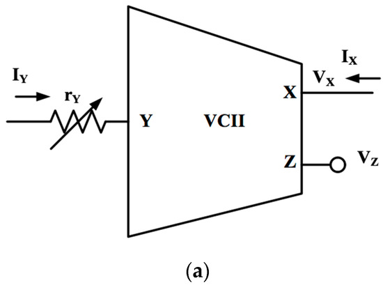
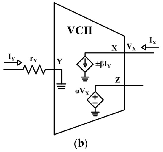
Figure 1.
VCII with electronic tunable impedance at the Y port: (a) symbolic representation; (b) internal structure.
In Equation (1), + and − indicate a VCII+ and a VCII−, respectively. There is a current buffer between the Y and X ports with a current gain of unity, while there is a voltage buffer between the X and Z ports with a voltage gain of unity. The resistance at the Y port is shown by rY, which is electronically tunable. We take advantage of the electronically tunable rY instead of adding an external passive resistor.
Figure 2 shows the schematic of the proposed VCII−-based BP/LP filter. It is composed of one VCII−, one external resistor, and two grounded capacitors. The internal resistance at Y is shown as rY, and is exploited to electronically vary the natural frequency of the filter. BP/LP outputs as voltage signals are produced at the Z port.
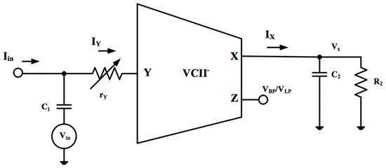
Figure 2.
The proposed VCII−-based second-order LP/ BP filter realization.
As can be seen in Figure 3, for Iin = 0, there will be a second-order BP transfer function. The analysis of the proposed BP circuit under ideal conditions is as follows:
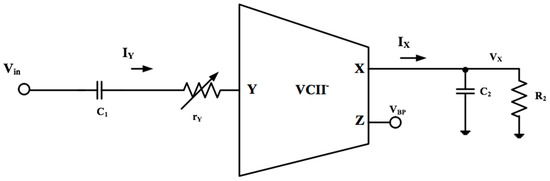
Figure 3.
The proposed VCII−-based second-order BP filter realization.
By assuming Y port at ground, for IY we have:
Using Equation (1):
Using Equations (2) and (3), VX is found as:
Using Equations (1) and (4), VBP is:
From Equation (5), ω0 and Q are found, respectively, as:
As can be seen from (6), the value of ω0 can be electronically tuned by varying rY.
If Vin = 0 and the input signal is applied as Iin, a second-order LP transfer function is achieved, as shown in Figure 4. A similar analysis gives the second-order LP transfer function as:

Figure 4.
The proposed VCII−-based second-order LP filter realization.
3. Non-Ideal Analysis
The operation of a VCII− in non-ideal conditions is given by Equation (9). Here, β and α are current gain between the Y and X terminals and voltage gain between the X and Z terminals, respectively. The main parasitic impedances associated with the VCII− ports are shown by rx (the parasitic resistance related to X port), Cx (parasitic capacitance related to X port) and rY (parasitic resistance related to Y port). The ideal values of rx and Cx are infinity and zero, respectively.
Figure 5 shows the proposed second-order BP filter in which all parasitic elements are modeled. Using Equation (9), the transfer function of Figure 5 is found as:
where:
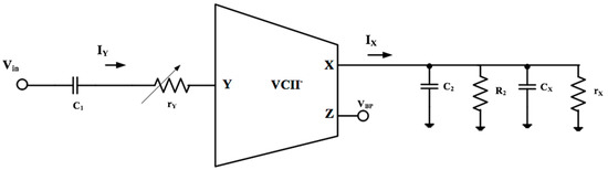
Figure 5.
The proposed second-order BP filter with VCII− non-ideal components.
From Equation (9), ω0 and Q are found, respectively, as:
Similar analysis for the proposed second-order LP filter gives:
4. CMOS Implementation of VCII− with Electronically Tunable Impedance at the Y Port
Figure 6 shows the CMOS implementation of VCII− with electronically tunable impedance at the Y port. It consists of 24 MOS transistors. Inversion of the current buffer comprising transistors M1–M6 is performed to transfer the Y port input current to the X port. The control current Icon is used to change the bias current of common gate transistor M2; therefore, electronically variable impedance at the Y port is provided. To maintain a constant bias current at the other branches, Icon is also applied to node 2; therefore, only the bias current of M2 is varied. In addition, to maintain a zero offset voltage at the Y port, bias currents of M1 and M2 must be kept equal, so Icon is also applied to node 1.
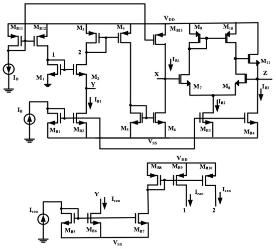
Figure 6.
CMOS implementation of VCII− with electronically variable impedance at the Y port. Nodes Y, 1 and 2 from the lower section of the schematic are connected to their counterparts in the upper section of the schematic.
The voltage buffer consists of transistors M7–M11, which are a differential pair cascaded by a voltage follower. They are connected in a closed loop configuration so as to decrease Z port impedance and improve the overall accuracy of the buffering action of transferring the X node voltage to the Z node. Transistors MBi for i = 1–12 provide the bias and control currents. The electronically variable impedance at the Y port is given by (with the usual meanings of the symbols):
5. Proposed LP/BP Second-Order Filter Simulation Results
PSpice simulations of the VCII− using 0.18 μm CMOS TSMC technology and a supply voltage of ±0.9 V are presented in Figure 6. The transistor sizes for the used PMOS and NMOS transistors were W = 9 µm, L = 0.9 µm and W = 27 µm, L = 0.9 µm, respectively. The values of bias currents were IB = IB1 = IB2 = IB3 = 20 µA. The control current Icon was varied from 0 μA to 50 μA. All bias currents were realized by simple current mirrors so as to ensure the best possible voltage swing at each terminal. To validate the proposed tuning technique, a comparison between the theoretical behavior of rY according to (15), and the values of the same magnitude extracted from the simulations is presented in Figure 7. In particular, µ = µelectrons = 0.13 m2/Vs, Cox = 9.51 × 10⁻⁴ F/m2 are constant values dependent on the technology. As can be seen, the trend between the theoretical and simulated curves matches, while the percentage error always remains below 10%. This error mirrors the inaccuracies of MB1, MB2 and MB5–MB10, which generate IB1 and Icon, directly impacting the simulated value of rY.
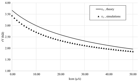
Figure 7.
Comparison between simulated and theoretical rY values as a function of Icon.
The large signal behavior of the used VCII was evaluated by extracting the slew rate (SR) figures both for the current output, X, and for the voltage output, Z. For the former, a ±20 µA step was used, which corresponds to the full ±IB range, while for the latter, a ±500 mV step was applied to the X terminal, with a 3 pF capacitive load at Z. The current slew rates were: SR+I = 13 × 103 A/s and SR−I = −0.64 × 10³ A/s, and the voltage slew rates were: SR+V = 1.4 × 10⁸ V/s and SR−V = −6.64 × 10⁶ V/s. As expected, the class A biasing of the input and output stages determines the difference between positive and negative values, with the latter remaining lower due to the sinking capability of the architecture being limited by the biasing current.
Table 1 shows the simulation results for the performance parameters and parasitic elements of the used VCII−.

Table 1.
The simulated characteristics of VCII− with electronically variable impedance at the Y port.
The proposed filter presented in Figure 2 was simulated using the VCII− presented in Figure 6. The values of the passive components were C1 = 100 pF, C2 = 10 pF and R2 = 5 kΩ. Figure 8 shows the AC frequency performance of the LP and BP outputs for different values of Icon. On the basis of the simulation results, ω0 was 1.2 MHz, 1.59 MHz and 1.7 MHz for Icon values of 0 μA, 25 μA and 50 μA, respectively. On the basis of Equation (12), the values of ω0 were 1.22 MHz, 1.54 MHz and 1.69 MHz, respectively. Fortunately, there is good agreement between the simulation and the calculation.
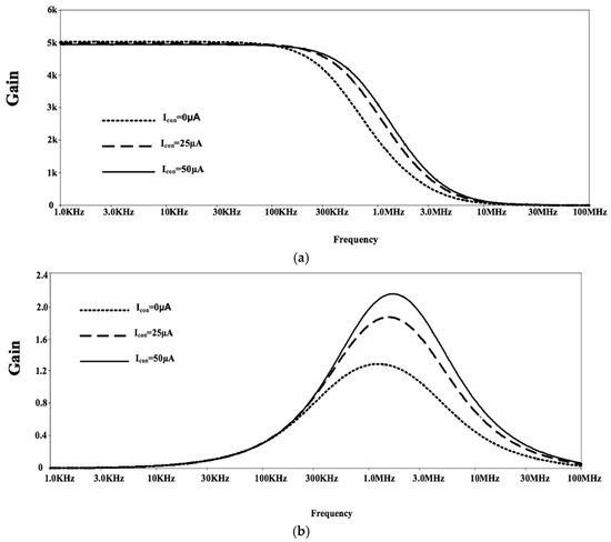
Figure 8.
Proposed circuit frequency performance for (a) LP and (b) BP outputs.
The robustness of the proposed solutions was tested by running 30 Monte Carlo (MC) simulations at each of the fast, typical, and slow corners. PVT combinations were as follows: SS, ±0.85 V, 80 °C; TT, ±0.9 V, 25 °C; FF, ±0.95 V, −20 °C, whereas for the MC analysis, we considered 3% mismatches in Vth and Cox of all transistors alongside a 5% variation in the value of the passive elements. The results are summarized in Table 2. As can be seen, the proposed circuit is robust against mismatches.
Table 2.
PVT and Monte Carlo simulation results for the magnitude of the filters and their ω0.
The linearity performance of the proposed circuit was checked for different values of Icon at ω0. The peak-to-peak values of Vin and Iin were 100 mV and 40 µA, respectively. The resulting THD is reported in Figure 9. As can be seen, the maximum value of THD remained below 4% and 8% for the LP and BP outputs, respectively.
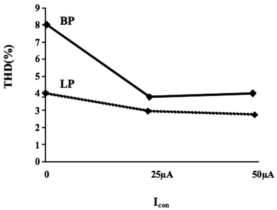
Figure 9.
The simulated THD for LP and BP outputs.
Finally, Figure 10 and Figure 11 show a time domain example of both the low-pass and band-pass filters. For the LP filter, an input current of 5 µA was used with frequencies of 100 kHz and 3 MHz. Icon was set to 50 µA. Similarly, for the BP, an input voltage of 10 mV was applied at three different frequencies, of 1.6 MHz, 1 MHz and 3 MHz. Icon was set equal to 50 µA.
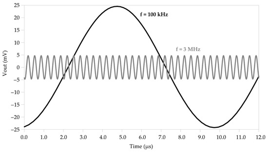
Figure 10.
Time domain output for the low-pass configuration.
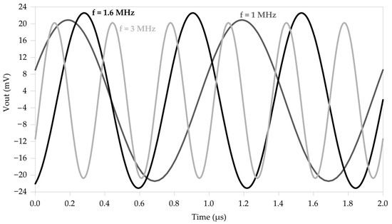
Figure 11.
Time domain output for the band-pass configuration.
Table 3 shows a comparison between the proposed circuit and others reported in the literature. As can be seen, the structures proposed in [1,3,13,14,15,16,17] provide output signal in current form, and therefore they are not suitable for applications requiring output signal in voltage form. In addition, the circuit of [3] requires an additional current buffer for practical use. The circuit reported in [10] produces output signal in voltage form; however, it needs extra voltage buffer at the output. Similarly, additional voltage buffer is necessary for the circuits presented in [17,19]. The circuits in [20,21] are not electronically tunable, and they suffer from a high supply voltage requirement. The VCII-based topology of [29] provides BP and LP outputs at the low-impedance Z port of VCII. Unfortunately, it is not electronically tunable. In contrast to other works, the proposed VCII-based circuit is electronically tunable, and does not require additional voltage buffers at the output node. More importantly, by taking advantage of the internal impedance at the Y port, the number of passive components is reduced.
Table 3.
Comparison between the proposed circuit and other reported works.
6. Conclusions
In this paper, a new realization of an electronically tunable second-order LP/BP filter using VCII− with the property of electronically tunable impedance at the Y port is presented. The proposed circuit consists of one VCII−, two capacitors, and one resistor. The output signal is in voltage form provided at the low-impedance Z port of the VCII, which makes it unnecessary to use extra voltage buffer in practical applications. The ω0 of the proposed transfer functions can be tuned using a control current (Icon), by means of which the impedance at the Y port of VCII can be varied. Therefore, the number of passive resistors used is also reduced, resulting in a simpler circuit and a reduced chip area. A non-ideal analysis is provided. Spice simulation results are reported to show the functionality of the proposed structure.
Author Contributions
Conceptualization, L.S.; Formal analysis, L.S.; Methodology, G.F.; Project administration, G.F. and V.S.; Resources, V.S.; Supervision, G.F. and V.S.; Visualization, G.B. and M.R.; Writing—original draft, L.S.; Writing—review & editing, G.B., G.F. and V.S. All authors have read and agreed to the published version of the manuscript.
Funding
This work was supported in part by the Italian Ministry of Education, University and Research (MIUR) with the research grant “ASSIOMI”, “PON R&I 2014–2020”.
Institutional Review Board Statement
Not applicable.
Informed Consent Statement
Not applicable.
Data Availability Statement
Data sharing not applicable. No new data were created or analyzed in this study. Data sharing is not applicable to this article.
Conflicts of Interest
The authors declare no conflict of interest.
References
- Sharma, A.; Maheshwari, S. Current follower based current mode filters. In Proceedings of the 2020 Third International Conference on Smart Systems and Inventive Technology (ICSSIT), Tirunelveli, India, 20–22 August 2020; pp. 632–636. [Google Scholar]
- Arora, T.S. Realization of current-mode universal filter utilising minimum active elements and only grounded passive components. In Proceedings of the 2020 7th International Conference on Signal Processing and Integrated Networks (SPIN), Noida, India, 27–28 February 2020; pp. 681–686. [Google Scholar]
- Ergun, E.; Ulutas, M. Low input impedance current-mode allpass and notch filter employing single current follower. In Proceedings of the 2007 14th International Conference on Mixed Design of Integrated Circuits and Systems, Ciechocinek, Poland, 21–23 June 2007; pp. 638–640. [Google Scholar]
- Safari, L.; Barile, G.; Stornelli, V.; Ferri, G.; Leoni, A. New current mode wheatstone bridge topologies with intrinsic linearity. In Proceedings of the 2018 14th Conference on Ph.D. Research in Microelectronics and Electronics (PRIME), Prague, Czech Republic, 2–5 July 2018; pp. 9–12. [Google Scholar]
- Safari, L.; Barile, G.; Stornelli, V.; Ferri, G. A New Versatile Full Wave Rectifier Using Voltage Conveyors. AEU—Int. J. Electron. Commun. 2020, 122, 153267. [Google Scholar] [CrossRef]
- Prommee, P.; Somdunyakanok, M.; Toomsawasdi, S. CMOS-based current-controlled DDCC and its applications. In Proceedings of the 2010 IEEE International Symposium on Circuits and Systems, Paris, France, 30 May–2 June 2010; pp. 1045–1048. [Google Scholar]
- Barile, G.; Safari, L.; Ferri, G.; Stornelli, V. A VCII-Based Stray Insensitive Analog Interface for Differential Capacitance Sensors. Sensors 2019, 19, 3545. [Google Scholar] [CrossRef] [PubMed]
- Sedra, A.; Smith, K. A Second-Generation Current Conveyor and Its Applications. IEEE Trans. Circuit Theory 1970, 17, 132–134. [Google Scholar] [CrossRef]
- Alzaher, H.A.; Elwan, H.; Ismail, M. A CMOS Fully Balanced Second-Generation Current Conveyor. IEEE Trans. Circuits Syst. II Analog. Digit. Signal Processing 2003, 50, 278–287. [Google Scholar] [CrossRef]
- Parveen, T.; Rajput, S.S.; Ahmad, M.T. Low Voltage CCII-based High Performance Cascadable Multifunctional Filter. Microelectron. Int. 2006, 23, 28–31. [Google Scholar] [CrossRef]
- Bhaskar, D.R.; Raj, A.; Kumar, P. Mixed-Mode Universal Biquad Filter Using OTAs. J. Circuit Syst. Comput. 2020, 29, 2050162. [Google Scholar] [CrossRef]
- Budboonchu, J.; Tangsrirat, W. Three-input single-output current-mode universal filter using single CCCTA. In Proceedings of the 2017 9th International Conference on Information Technology and Electrical Engineering (ICITEE), Phuket, Thailand, 12–13 October 2017; pp. 1–4. [Google Scholar]
- Duangmalai, D.; Jaikla, W. Resistorless current-mode universal filter using current differencing cascaded transconductance amplifiers. In Proceedings of the 2018 3rd International Conference on Control and Robotics Engineering (ICCRE), Nagoya, Japan, 20–23 April 2018; pp. 188–191. [Google Scholar]
- Stornelli, V.; Pantoli, L.; Leuzzi, G.; Ferri, G. Fully Differential DDA-Based Fifth and Seventh Order Bessel Low Pass Filters and Buffers for DCR Radio Systems. Analog Integr. Circuits Signal Process. 2013, 75, 305–310. [Google Scholar] [CrossRef]
- Lamun, P.; Phatsornsiri, P.; Torteanchai, U. Single VDCC-based current-mode universal biquadratic filter. In Proceedings of the 2015 7th International Conference on Information Technology and Electrical Engineering (ICITEE), Chiang Mai, Thailand, 29–30 October 2015; pp. 122–125. [Google Scholar]
- Torteanchai, U.; Kumngern, M. Three-input single-output current-mode universal filter using a single FDCCII and grounded passive components. In Proceedings of the 2014 International Symposium on Intelligent Signal Processing and Communication Systems (ISPACS), Kuching, Malaysia, 1–4 December 2014; pp. 275–278. [Google Scholar]
- Chen, H.-P. Tunable Versatile Current-Mode Universal Filter Based on plus-Type DVCCs. AEUE—Int. J. Electron. Commun. 2012, 4, 332–339. [Google Scholar] [CrossRef]
- Singh, S.; Maheshwari, S.; Mohan, J.; Chauhan, D.S. Electronically tunable current-mode universal biquad filter based on the CCCCTA. In Proceedings of the 2009 International Conference on Advances in Recent Technologies in Communication and Computing, Kottayam, India, 27–28 October 2009; pp. 424–429. [Google Scholar]
- Horng, J.W.; Chou, P.-Y.; Wu, J.-Y. Voltage/Current-Mode Multifunction Filters Using Current-Feedback Amplifiers and Grounded Capacitors. Act. Passiv. Electron. Compon. 2010, 2010, e785631. [Google Scholar] [CrossRef]
- Arora, T.S.; Rana, U. Multifunction Filter Employing Current Differencing Buffered Amplifier. Circuits Syst. 2016, 7, 543–550. [Google Scholar] [CrossRef]
- Sagbas, M.; Koksal, M. A New multi-mode multifunction filter using CDBA. In Proceedings of the 2005 European Conference on Circuit Theory and Design, Cork, Ireland, 2 September 2005; Volume 2, pp. II/225–II/228. [Google Scholar]
- Safari, L.; Barile, G.; Stornelli, V.; Ferri, G. An Overview on the Second Generation Voltage Conveyor: Features, Design and Applications. IEEE Trans. Circuits Syst. II: Express Briefs 2019, 66, 547–551. [Google Scholar] [CrossRef]
- Čajka, J.; Vrba, K. The Voltage Conveyor May Have in Fact Found Its Way into Circuit Theory. AEU—Int. J. Electron. Commun. 2004, 58, 244–248. [Google Scholar] [CrossRef]
- Barile, G.; Safari, L.; Ferri, G.; Stornelli, V. Traditional Op-Amp and New VCII: A Comparison on Analog Circuits Applications. AEU—Int. J. Electron. Commun. 2019, 110, 152845. [Google Scholar] [CrossRef]
- Pantoli, L.; Barile, G.; Leoni, A.; Muttillo, M.; Stornelli, V. Electronic Interface for Lidar System and Smart Cities Applications. J. Commun. Softw. Syst. 2019, 15, 118–125. [Google Scholar] [CrossRef]
- Al-Absi, M. Realization of inverse filters using second generation voltage conveyor (VCII). Analog Integr. Circuits Signal Process. 2021, 109, 29–32. [Google Scholar] [CrossRef]
- Stornelli, V.; Safari, L.; Barile, G.; Ferri, G. A New Extremely Low Power Temperature Insensitive Electronically Tunable VCII-Based Grounded Capacitance Multiplier. IEEE Trans. Circuits Syst. II: Express Briefs 2021, 68, 72–76. [Google Scholar] [CrossRef]
- Stornelli, V.; Ferri, G. A 0.18μm CMOS DDCCII for Portable LV-LP Filters. Radioengineering 2013, 22, 434–439. [Google Scholar]
- Safari, L.; Barile, G.; Ferri, G.; Stornelli, V. High Performance Voltage Output Filter Realizations Using Second Generation Voltage Conveyor. Int. J. RF Microw. Comput.-Aided Eng. 2018, 28, e21534. [Google Scholar] [CrossRef]
Publisher’s Note: MDPI stays neutral with regard to jurisdictional claims in published maps and institutional affiliations. |
© 2022 by the authors. Licensee MDPI, Basel, Switzerland. This article is an open access article distributed under the terms and conditions of the Creative Commons Attribution (CC BY) license (https://creativecommons.org/licenses/by/4.0/).