Article

An 11-Bit 10 MS/s SAR ADC with C–R DAC Calibration and Comparator Offset Calibration

1
Department of Electronic Engineering, Kumoh National Institute of Technology, Gumi 39177, Korea
2
DDI Design Team, DB Hitek, 90, Sudo-ro, Bucheon 14519, Korea
*
Author to whom correspondence should be addressed.
Electronics 2022, 11(22), 3654; https://doi.org/10.3390/electronics11223654
Submission received: 19 October 2022 / Revised: 4 November 2022 / Accepted: 7 November 2022 / Published: 9 November 2022
(This article belongs to the Special Issue Mixed Signal Circuit Design)

Abstract

:
An 11-bit 10 MS/s successive approximation register (SAR) analog-to-digital converter (ADC) is proposed for low-power and small-area applications. A 10-bit differential capacitor–resistor (C–R) digital-to-analog converter (DAC) is used to minimize the area of a DAC. The use of a C–R DAC reduces the capacitor area of a SAR ADC used CDAC by 75%. A capacitor calibration for the upper 5-bit capacitors of the C–R DAC is proposed to increase the linearity of the C–R DAC. To evaluate the proposed SAR ADC, an 11-bit 10 MS/s SAR ADC is implemented using a 180 nm 1-poly six-metal CMOS process with a supply of 1.8 V. The proposed SAR ADC has an effective number of bits (ENOBs) of 10.3 bits at a sampling rate of 10 MS/s for a 3.6-VPP differential sinusoidal analog input with a frequency of 4.789 MHz. The measured ENOBs is 10.45 bits when the frequency of the analog input signal is 42.39 kHz. The proposed C–R DAC calibration including comparator offset calibration improves the performances of differential nonlinearity (DNL) and integral nonlinearity (INL) from −1/+1.26 LSBs and −1.98/+1.96 LSBs to −0.97/+0.85 LSBs and −0.79/+0.83 LSBs, respectively.

1. Introduction

Recently, analog-to-digital converters (ADCs) used in various fields including mobile applications require low power, high resolution, and low area characteristics. A successive approximation register (SAR) ADC has a suitable structure for low-power design because it uses only capacitors, switches, logics, and one comparator without an amplifier consuming a static current [1,2,3,4,5]. However, as the resolution of the SAR ADC increases, the number and area of capacitors increase proportionally to the power of two of the resolutions [6]. A capacitor–resistor DAC (C–R DAC) combined a capacitor digital-to-analog converter (CDAC) and a resistor digital-to-analog converter (RDAC) can be used to reduce the area that increases with increasing resolution of the SAR ADC [7]. Although the SAR ADC uses a C–R DAC to reduce the area, in order to further reduce the area and power consumption of the DAC for the SAR ADC, the unit capacitor of the CDAC generally uses the minimum capacitor which is supported by the CMOS process. In this case, capacitor values are sensitive to process variations and parasitic components [8,9,10]. The mismatch between capacitors used in the CDAC deteriorates the performances of not only the CDAC but also the SAR ADC. A capacitor calibration of a CDAC has been reported for the improvement of a SAR ADC [11,12,13,14,15]. This capacitor calibration for the CDAC requires an accurate comparator that can sense voltages less than 1 LSB without an offset voltage [16].
In this paper, an 11-bit 10 MS/s SAR ADC is designed to be implemented in a small area using a C–R DAC. The C–R DAC calibration including the comparator offset calibration is proposed for the performance improvement of the SAR ADC. Section 2 describes the architecture and operation of the SAR ADC proposed in this paper. Section 3 explains the proposed C–R DAC calibration including comparator offset calibration. Section 4 presents the implementation and measurement results of the SAR ADC. Finally, Section 5 provides the conclusion of this paper.

2. Design of 11-Bit 10 MS/s SAR ADC Using C–R DAC

Figure 1a shows the block diagram of the proposed 11-bit 10 MS/s SAR ADC. A C–R DAC, a comparator with calibration of offset voltage, and a SAR logic with calibration logic and voting logic are used for the proposed SAR ADC.
The C–R DAC samples the analog input signal and also performs a subtraction operation between the sampled analog value and the reference voltage generated according to the SAR operation. The C–R DAC has an architecture that combines a VCM-based 8-bit CDAC with a 2-bit RDAC. Since the 2-bit RDAC drives only the LSB capacitor (C0) of the CDAC, it is designed for low power even when supplying the reference voltage. Table 1 shows the number of capacitors used in the DAC for the 11-bit SAR ADC. When a CDAC and a C–R DAC are used for the DAC for the 11-bit SAR ADC, capacitors of 2048·C and 512·C are used, respectively. The C–R DAC can reduce the capacitor area of the DAC by 75% compared to the CDAC.
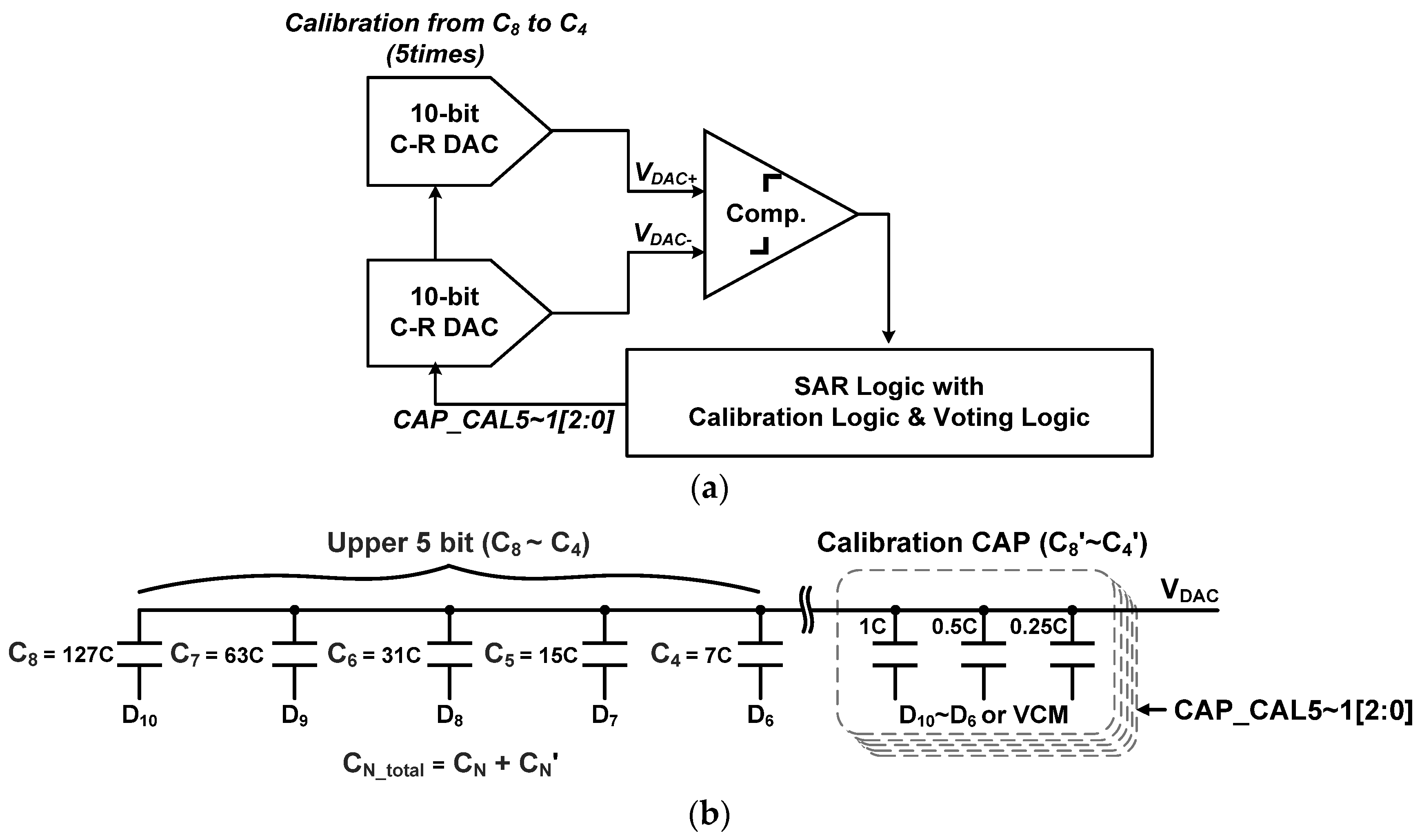
The calibration capacitors (C8′–C4′) are additionally used to reduce the mismatch occurring in the upper 5-bit capacitor (C8–C4) of the 8-bit CDAC. The comparator has an architecture of a sense-amplifier-based voltage comparator and includes a meta-stability detector for stable asynchronous SAR operation [17]. The comparator compares the differential output voltages of the C–R DACs to each other. For the operation of the asynchronous SAR ADC, it uses the VALID signal indicating the completion of the current comparison operation as a synchronization signal for the next comparison operation. The capacitor calibration logic determines the 15-bit digital code (CAP_CAL5[2:0], ···, CAP_CAL1[2:0]) by the proposed C–R DAC calibration and supplies it to the calibration capacitors.
Figure 1b shows the timing diagram of the proposed SAR ADC. When the sample signal of the SAR logic is high, the differential analog input (VINP and VINM) is sampled to the bottom plates of the capacitors of the CDAC, and the VCM voltage is supplied to the top plates of the capacitors. This sample operation is finished in synchronization with the rising edge of the EXCLK. When the sample operation is completed, the VCM is supplied to the bottom plates of the capacitors, and VDAC+ and VDAC- are output on the top plates of the capacitors of the CDAC. The comparator compares VDAC+ and VDAC- in synchronization with the CLKC. When the comparison is completed, the comparator outputs the VALID signal to high and stores the comparison result in the register in synchronization with VALID. In addition, the SAR logic generates a control signal for reference generation for the next conversion of the C–R DAC using the result of the comparison and turns the CLKC and VALID signals low. This process is repeated 11 times to generate an 11-bit digital code, and the next sample operation is performed in synchronization with the rising edge of the last VALID.

3. Proposed C–R DAC Calibration and Comparator Offset Calibration

Figure 2 shows a transfer curve of the CDAC. The gray line of the transfer curve is the ideal analog output, and the black line is the analog output generated by the real DAC. The capacitor mismatch in the CDAC worsens its linearity characteristics, as shown in Figure 2a. In this case, as indicated by the red line, overlapping analog voltages or missing analog voltages may be generated as the digital code increases. Figure 2b shows the transfer curve of the CDAC when the mismatch between capacitors in CDAC is ideally calibrated. In this case, the CDAC output outputs a monotonic analog signal, and its output value has quantized analog voltages at regular intervals. As a result, the linearity properties of the CDAC such as differential non-linearity (DNL) and integral non-linearity (INL) are improved. In general, the mismatch of the capacitor corresponding to the upper bit of the CDAC greatly worsens the DNL and INL of the CDAC more than the mismatch of the capacitor corresponding to the LSB. Thus, the proposed C–R DAC calibration calibrates the capacitors of the upper five bits in this work.
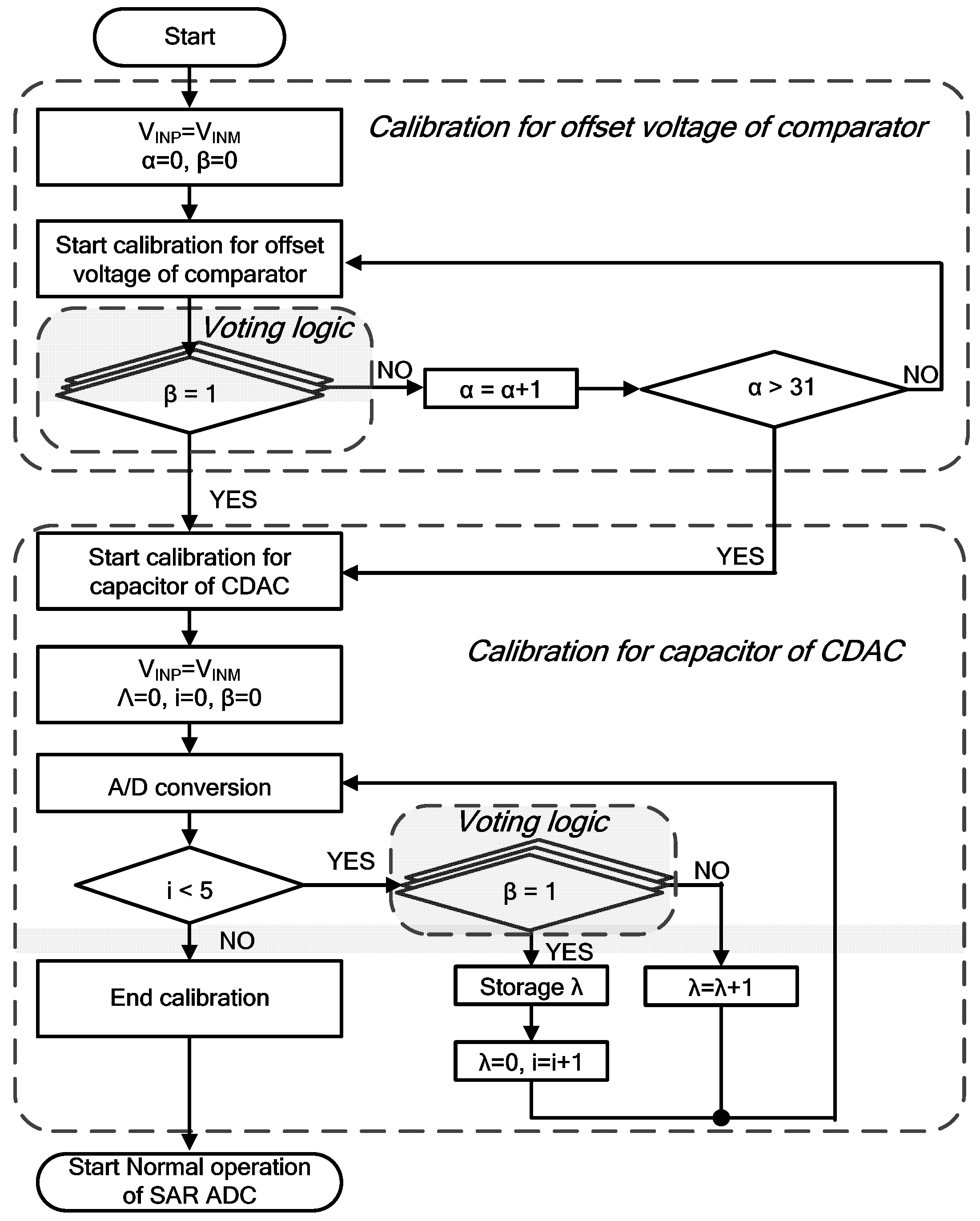
Figure 3 shows the sequence of performing the C–R DAC calibration for the linearity of the SAR ADC. First of all, since the proposed C–R DAC calibration is performed according to the output of the comparator used in the SAR ADC, it is necessary to remove the comparator offset voltage before this calibration. The VINP and VINM are analog inputs of the C–R DAC and are sampled to the same value. α and β mean the calibration code of the comparator offset calibration and the comparison result of the comparator. α is actually implemented as a binary 5-bit code in this work. However, it is expressed in decimal code for convenience in Figure 3. α and β have an initial value of 0. During β is 0, the comparator offset calibration continues and α is increased by 1. When β becomes 1, the comparator offset calibration is completed, and the value of α is stored as the calibration code of the comparator offset calibration. After the comparator offset calibration, the C–R DAC calibration is started. The C–R DAC differentially samples a voltage of zero as the differential input signal. i is an index indicating the calibration of the upper 5-bit capacitors of the C–R DAC, and λ and β are a capacitor calibration code and the comparison result of the comparator, respectively. The initial values of these three values are both 0. The C–R DAC calibration is performed similarly to the comparator offset calibration. To improve the comparison performance in the C–R DAC calibration and the comparator offset calibration, the result of the comparator is determined by a voting process [18,19].

3.1. C–R DAC Calibration

Figure 4a shows the concept of calibration for the upper 5-bit capacitors of the C–R DAC [14]. The comparator offset calibration is performed by the sequence shown in Figure 3. The calibration codes (CAP_CAL#[2:0]) are sequentially increased and stored by the control of the SAR logic with calibration logic and voting logic until the comparator outputs a high. The calibration process is performed five times to calibrate capacitors C8 to C4. Figure 4b shows the block diagram of calibration for upper 5-bit capacitors of C–R DAC. The proposed C–R DAC consists of an 8-bit CDAC, a 2-bit RDAC, and a calibration capacitor. Each capacitor of the upper 5-bit capacitors is determined by the sum of CN and CN’. The calibration capacitor is composed of a minimum unit of 0.25C, so the capacitor calibration of the C–R DAC is performed with a resolution of 1/4 LSB.

3.2. Comparator Offset Calibration

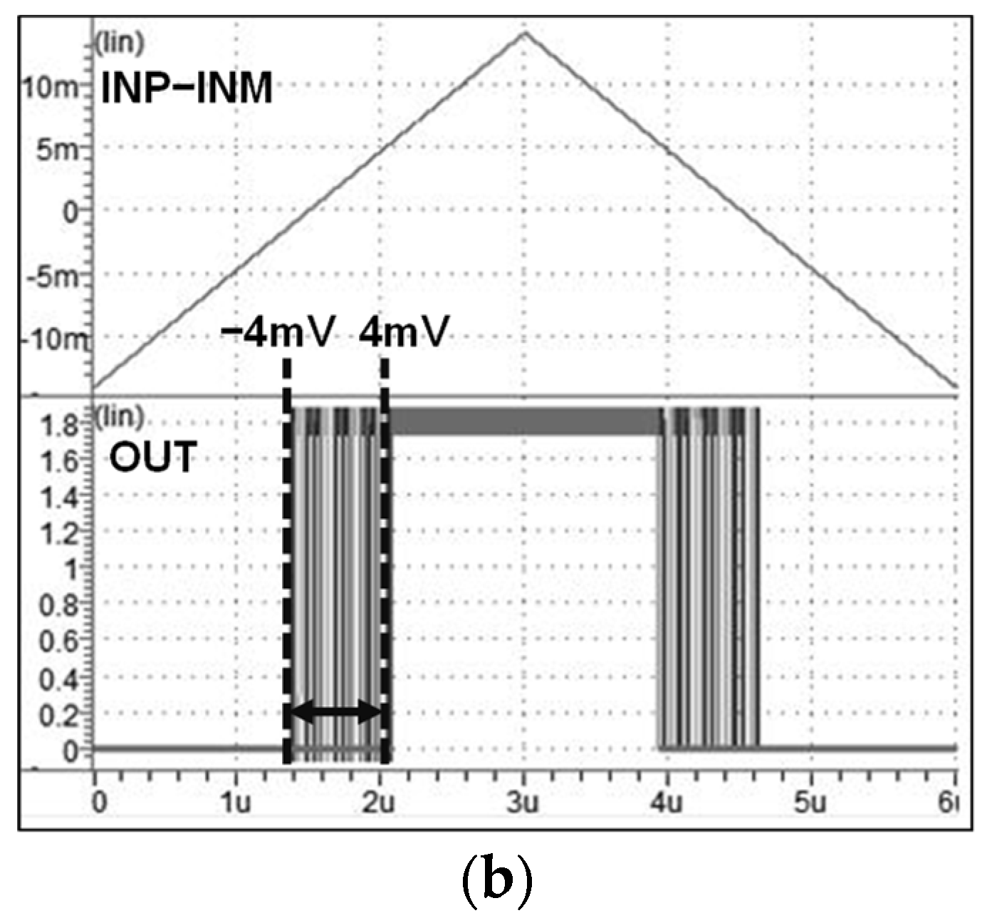
Figure 5a shows the circuit diagram of the comparator with a pre-amplifier and offset-calibration circuit. The comparator has an architecture of a sense-amplifier-based voltage comparator and includes a pre-amplifier and an offset-calibration circuit to remove the comparator offset voltage while increasing the voltage gain of the comparator. The 5-bit RDAC is used to supply an offset voltage into the offset-calibration circuit. The comparator senses the operational results of (INP − INM) + (OFFSETINP − OFFSETINM) using a pre-amplifier and an offset-calibration circuit and outputs its result to the CMOS voltage level. The comparator offset voltage is removed by the difference voltage between OFFSETINP and OFFSETINM generated by the comparator offset calibration code OFFSET [4:0] in the 5-bit RDAC. Figure 5b shows a simulation result about the calibration voltage range of the comparator offset voltage. The calibration voltage range designed in this work is about −4 mV to 4 mV, and the calibration resolution voltage is about 0.2 mV, considering the voltage of 1 LSB.

3.3. Voting Logic

The calibration code of the proposed C–R DAC calibration is determined based on the comparison results of the comparator. Thus, the comparator needs to compare a voltage lower than the voltage of 1 LSB even if there is dynamic noise such as power supply noise and various switching noises. In this work, the comparator performs a voting process for accurate comparison in the C–R DAC calibration. In the voting process, the comparator performs three comparisons for the same analog voltage, and the final result is determined by the majority result. Figure 6a shows the block diagram of the voting logic. The voting logic consists of three flip-flops and some static logics. The two comparator outputs are sampled at the rising edge of OCLKB_LSB [2] and OCLKB_LSB [1], respectively. The voting process proceeds as the two sampled signals, Q1 and Q2, are logically operated together with the final third comparator output COMP_OUT. This result is sampled at the rising edge of the final OCLKB_LSB and output as the result of the voting process, as shown in Figure 6b.

4. Chip Implement and Measurement Results

The proposed 11-bit 10 MS/s SAR ADC was designed using a 180 nm CMOS process with a 1.8-V supply voltage. The CMOS process used in this work supports a metal-insulator–metal capacitor of at least 25 fF for the unit capacitor of the C–R DAC. The active area of the proposed 11-bit 10 MS/s SAR ADC is 650 μm × 450 μm, as shown in Figure 7. It was reduced by the use of the C–R DAC. The SAR ADC with a full rail-to-rail input voltage range consumes 583 μW of power when operating at a sampling rate of 10 MHz.
Figure 8 shows the test environment for the implemented SAR ADC. The analog differential input signal and clock signal were sourced from NI PXIe-5451. In addition, Audio Precision equipment was used to supply an analog input signal with a low frequency. The digital output code of the implemented SAR ADC was acquired using NI PXIe-6556. The performance of the 11-bit 10 MS/s SAR ADC was analyzed through signal processing using LabVIEW software for the acquired digital output code.
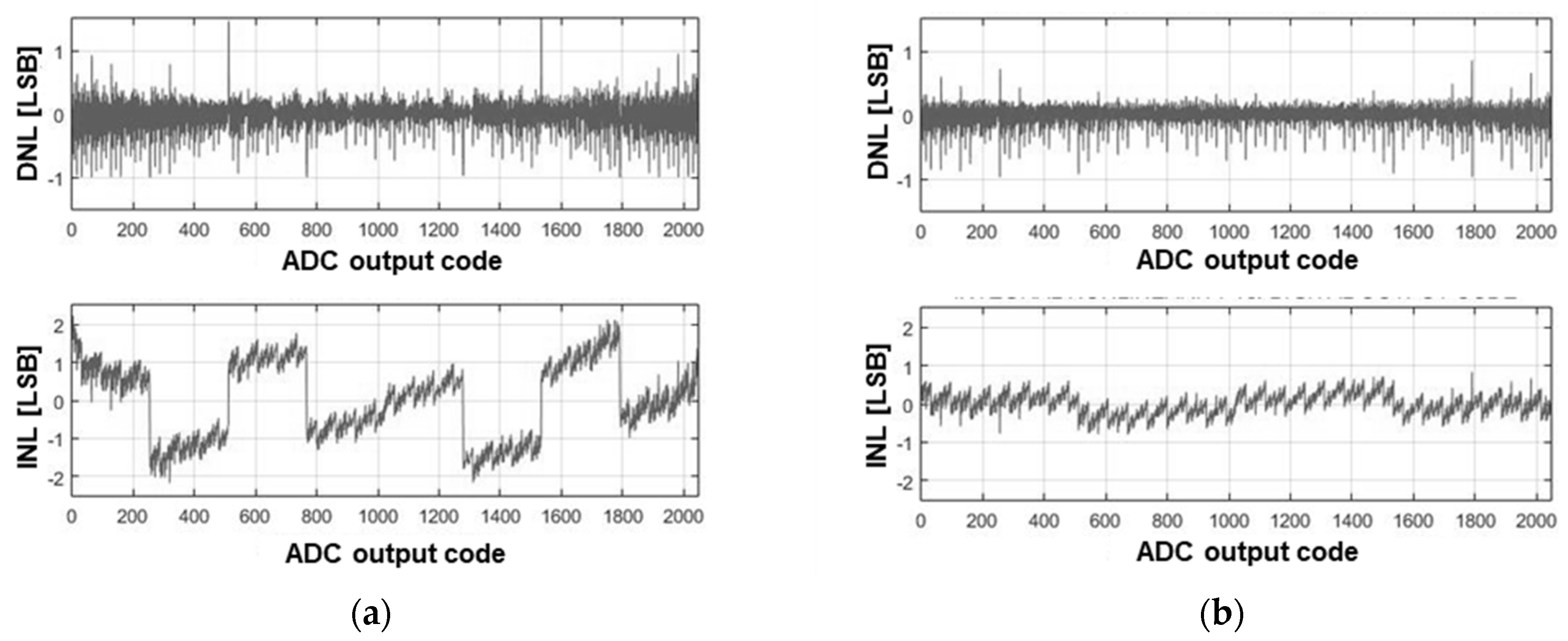
Figure 9 shows the measured static performances of the proposed 11-bit 10-MS/s SAR ADC according to the C–R DAC calibration. As shown in the measurement results, the proposed C–R DAC calibration improves the performances of DNL and INL from −1/+1.26 LSBs and −1.98/+1.96 LSBs to −0.97/+0.85 LSBs and −0.79/+0.83 LSBs. Figure 10 shows the measured dynamic performances of the proposed SAR ADC for an analog input signal with a low frequency of 42.39 kHz. The performances of signal-to-noise and distortion ratio (SNDR) and the effective number of bits (ENOBs) were improved from 57.93 dB and 9.33 bits to 64.71 dB and 10.45 bits by the proposed C–R DAC calibration. The proposed C–R DAC calibration improved the ENOB of 0.99 bits even for an analog input signal with a Nyquist frequency of 4.78 MHz, as shown in Figure 11. As a result, the proposed SAR ADC has an ENOB of 10.3 bits at the Nyquist frequency.
Table 2 shows the performance comparison of SAR ADCs. The proposed 11-bit 10 MS/s SAR ADC has an ENOB performance comparable to the previous literature [20,21,22,23] at the Nyquist frequency.

5. Conclusions

The 11-bit 10 MS/s SAR ADC with C–R DAC calibration for the upper 5-bits and comparator offset calibration was proposed for mobile applications requiring small areas and low power consumption. The capacitor calibration for the upper 5-bits of the C–R DAC simplifies the control logic by only performing the process of increasing the capacitor for the upper 5-bits. The proposed C–R DAC calibration, including comparator offset calibration and voting process, improved the linearity performance of the SAR ADC. The proposed SAR ADC was fabricated using a 180 nm 1-poly six-metal CMOS process with a 1.8-V supply voltage. The ENOB of the SAR ADC using the C–R DAC calibration was improved from 9.31 bits to 10.30 bits for an analog input signal with a Nyquist frequency of 4.789 MHz. Furthermore, the proposed C–R DAC calibration including comparator offset calibration improved the performances of DNL and INL from −1/+1.26 LSBs and −1.98/+1.96 LSBs to −0.97/+0.85 LSBs and −0.79/+0.83 LSBs.

Author Contributions

Conceptualization, H.J., E.Y. and Y.-C.J.; Design, implementation, H.J. and E.Y.; measurement, H.J.; Writing and editing, all authors; Supervision, Y.-C.J.; Funding acquisition, Y.-C.J. All authors have read and agreed to the published version of the manuscript.

Funding

This work was supported by the Grand Information Technology Research Center Program (IITP-2020-2020-0-01612) through the IITP and the Commercializations Promotion Agency for R&D Outcomes (COMPA) grant (No. 2021I100) funded by the MSIT, and the Basic Science Research Program (2020R1I1A3071634) through the NRF funded by the Ministry of Education, Korea.

Informed Consent Statement

Informed consent was obtained from all subjects involved in the study.

Acknowledgments

The EDA tool was supported by the IC Design Education Center, Korea.

Conflicts of Interest

The authors declare no conflict of interest. The funders had no role in the design of the study; in the collection, analyses, or interpretation of data; in the writing of the manuscript, or in the decision to publish the results.

References

  1. Choi, S.; Ku, H.-S.; Son, H.; Kim, B.; Park, H.-J.; Sim, J.-Y. An 84.6-dB-SNDR and 98.2-dB-SFDR Residue-Integrated SAR ADC for Low-Power Sensor Applications. IEEE J. Solid-State Circuits 2018, 53, 404–417. [Google Scholar] [CrossRef]
  2. Zhang, D.; Bhide, A.; Alvandpour, A. A 53-nW 9.1-ENOB 1-kS/s SAR ADC in 0.13-μm CMOS for Medical Implant Devices. IEEE J. Solid-State Circuits 2012, 47, 1585–1593. [Google Scholar] [CrossRef] [Green Version]
  3. Harpe, P.J.A.; Zhou, C.; Bi, Y.; van der Meijs, N.P.; Wang, X.; Philips, K.; Dolmans, G.; de Groot, H. A 26 μW 8 bit 10 MS/s Asynchronous SAR ADC for Low Energy Radios. IEEE J. Solid-State Circuits 2011, 46, 1585–1595. [Google Scholar] [CrossRef]
  4. Liu, C.; Kuo, C.; Lin, Y. A 10 bit 320 MS/s Low-Cost SAR ADC for IEEE 802.11ac Applications in 20 nm CMOS. IEEE J. Solid-State Circuits 2015, 50, 2645–2654. [Google Scholar] [CrossRef]
  5. Guo, W.; Kim, Y.; Tewfik, A.H.; Sun, N. A Fully Passive Compressive Sensing SAR ADC for Low-Power Wireless Sensors. IEEE J. Solid-State Circuits 2017, 52, 2154–2167. [Google Scholar] [CrossRef]
  6. Liu, S.; Rabuske, T.; Paramesh, J.; Pileggi, L.; Fernandes, J. Analysis and Background Self-Calibration of Comparator Offset in Loop-Unrolled SAR ADCs. IEEE Trans. Circuits Syst. I Regul. Pap. 2017, 65, 458–470. [Google Scholar] [CrossRef]
  7. Zhou, H.; Gui, X.; Gao, P. Design of a 12-bit 0.83 MS/s SAR ADC for an IPMI SoC. In Proceedings of the 2015 28th IEEE International System-on-Chip Conference, Beijing, China, 8–11 September 2015; pp. 175–179. [Google Scholar]
  8. Zhang, C.; Wang, H. Reduction of Parasitic Capacitance Impact in Low-Power SAR ADC. IEEE Trans. Instrum. Meas. 2011, 61, 587–594. [Google Scholar] [CrossRef]
  9. Um, J.; Kim, Y.; Song, E.; Sim, J.; Park, H. A Digital-Domain Calibration of Split-Capacitor DAC for a Differential SAR ADC Without Additional Analog Circuits. IEEE Trans. Circuits Syst. I Regul. Pap. 2013, 60, 2845–2856. [Google Scholar] [CrossRef]
  10. Zhang, M.; Noh, K.; Fan, X.; Sánchez-Sinencio, E. A 0.8–1.2 V 10–50 MS/s 13-bit Subranging Pipelined-SAR ADC Using a Temperature-Insensitive Time-Based Amplifier. IEEE J. Solid-State Circuits 2017, 52, 2991–3005. [Google Scholar] [CrossRef]
  11. Zhu, Y.; Chan, C.; Wong, S.; Seng-Pan, U.; Martins, R.P. Histogram-Based Ratio Mismatch Calibration for Bridge-DAC in 12-bit 120 MS/s SAR ADC. IEEE Trans. Very Large Scale Integr. VLSI Syst. 2015, 24, 1203–1207. [Google Scholar] [CrossRef]
  12. Wang, X.; Li, F.; Wang, Z. A Simple Histogram-Based Capacitor Mismatch Calibration in SAR ADCs. IEEE Trans. Circuits Syst. II Express Briefs 2020, 67, 2838–2842. [Google Scholar] [CrossRef]
  13. Yoshioka, M.; Ishikawa, K.; Takayama, T.; Tsukamoto, S. A 10-b 50-MS/s 820-uW SAR ADC With On-Chip Digital Calibration. IEEE Trans. Biomed. Circuits Syst. 2010, 2010, 410–416. [Google Scholar] [CrossRef] [PubMed]
  14. Youn, E.; Jang, Y.-C. 12-bit 20M-S/s SAR ADC using C-R DAC and Capacitor Calibration. In Proceedings of the 2018 International SoC Design Conference (ISOCC), Deagu, Korea, 12–15 November 2018; pp. 2163–9612. [Google Scholar]
  15. Lee, S.-Y.; Tsou, C.; Li, Y.-C. Single-Bin DFT-Based Digital Calibration Technique for CDAC in SAR ADCs. IEEE Trans. Circuits Syst. I Regul. Pap. 2019, 66, 4582–4591. [Google Scholar] [CrossRef]
  16. Peng, X.; Gao, A.; Chen, Z.; Zhang, H.; Li, Y.; Cao, W.; Liu, X.; Tang, H. A Novel Comparator Offset Calibration Technique for SAR ADCs. In Proceedings of the 2018 IEEE International Conference on Electron Devices and Solid State Circuits (EDSSC), Shenzhen, China, 6–8 June 2018. [Google Scholar]
  17. Park, S.-M.; Jeong, Y.-H.; Hwang, Y.-J.; Lee, P.-H.; Kim, Y.-W.; Son, J.; Lee, H.-Y.; Jang, Y.-C. A 10-bbit 20-MS/s Asynchronous SAR ADC with Meta-Stability Detector Using Replica Comparators. IEICE Trans. Electron. 2016, 99, 651–654. [Google Scholar] [CrossRef]
  18. Harpe, P.; Cantatore, E.; Roermund, A.V. An oversampled 12/14b SAR ADC with noise reduction and linearity enhancements achieving up to 79.1 dB SNDR. In Proceedings of the 2014 IEEE International Solid-State Circuits Conference Digest of Technical Papers, San Francisco, CA, USA, 9–13 February 2014. [Google Scholar]
  19. Harpe, P.; Cantatore, E.; Roermund, A.V. A 10b/12b 40kS/s SAR ADC With Data-Driven Noise Reduction Achieving up to 10.1b ENOB at 2.2 fJ/Conversion-Step. IEEE J. Solid-State Circuits 2013, 48, 3011–3018. [Google Scholar] [CrossRef]
  20. Zhou, Y.; Xu, B.; Chiu, Y. A 12 bit 160 MS/s Two-Step SAR ADC With Background Bit-Weight Calibration Using a Time-Domain Proximity Detector. IEEE J. Solid-State Circuits 2015, 50, 920–931. [Google Scholar] [CrossRef]
  21. Liu, W.; Huang, P.; Chiu, Y. A 12-bit 50-MS/s 3.3-mW SAR ADC with background digital calibration. In Proceedings of the IEEE 2012 Custom Integrated Circuits Conference, San Jose, CA, USA, 9–12 September 2012. [Google Scholar]
  22. Chan, C.; Zhu, Y.; Li, C.; Zhang, W.; Ho, I.; Wei, L.; Seng-Pan, U.; Martins, R.P. 60-dB SNDR 100-MS/s SAR ADCs With Threshold Reconfigurable Reference Error Calibration. IEEE J. Solid-State Circuits 2017, 52, 2576–2588. [Google Scholar] [CrossRef]
  23. Bindra, H.S.; Annema, A.; Simon, M.L.; Nauta, B. A 0.2–8 MS/s 10b flexible SAR ADC achieving 0.35–2.5 fJ/conv-step and using self-quenched dynamic bias comparator. In Proceedings of the 2019 Symposium on VLSI Circuits, Kyoto, Japan, 9–14 July 2019. [Google Scholar]
Figure 1. Proposed SAR ADC: (a) block diagram; (b) timing diagram.
Electronics 11 03654 g001
Figure 2. Transfer curves of CDAC: (a) with capacitor mismatch in CDAC; (b) after capacitor calibration in CDAC.
Electronics 11 03654 g002
Figure 3. Sequence of C–R DAC calibration including comparator offset calibration.
Electronics 11 03654 g003
Figure 4. Calibration for upper 5-bit capacitors of C–R DAC: (a) concept; (b) block diagram.
Electronics 11 03654 g004
Figure 5. Comparator with offset voltage calibration: (a) circuit diagram; (b) simulation results.
Electronics 11 03654 g005aElectronics 11 03654 g005b
Figure 6. Voting logic: (a) block diagram; (b) timing diagram.
Electronics 11 03654 g006
Figure 7. Chip photograph of implemented 11-bit SAR ADC.
Electronics 11 03654 g007
Figure 8. Test environment of implemented 11-bit SAR ADC.
Electronics 11 03654 g008
Figure 9. Measured static performances of 11-bit SAR ADC: (a) before C–R DAC calibration; (b) after C–R DAC calibration.
Electronics 11 03654 g009
Figure 10. Measured dynamic performances of 11-bit SAR ADC at a differential analog input signal with low frequency of 42.39 kHz: (a) before C–R DAC calibration; (b) after C–R DAC calibration.
Electronics 11 03654 g010
Figure 11. Measured dynamic performances of 11-bit SAR ADC at a differential analog input signal with Nyquist frequency of 4.78 MHz: (a) before C–R DAC calibration; (b) after C–R DAC calibration.
Electronics 11 03654 g011
Table 1. Capacitors used in DAC for 11-bit SAR ADC.
ItemCDACC–R DAC
CDAC2048·C512·C
Table 2. Performance comparison of SAR ADCs.
Item[20][21][22][23]This Work
ArchitecturePipelined SAR SARSARSARSAR
CalibrationYesYesYesNoYes
Resolution [bit]1212111011
Technology [nm]40906565180
Supply [V]1.11.21.21.31.8
FS [MHz]16050100810
Power [μW]49604700244012.8583
Area [mm2]0.0420.1180.0120.040.29
SFDR [dB]86.982.768.356678.57
SNDR [dB]65.365.157.9357.7463.77
ENOB [bits]10.510.59.339.310.3
Publisher’s Note: MDPI stays neutral with regard to jurisdictional claims in published maps and institutional affiliations.