
An Investigation into the Comprehensive Impact of Self-Heating and Hot Carrier Injection


Abstract
:1. Introduction
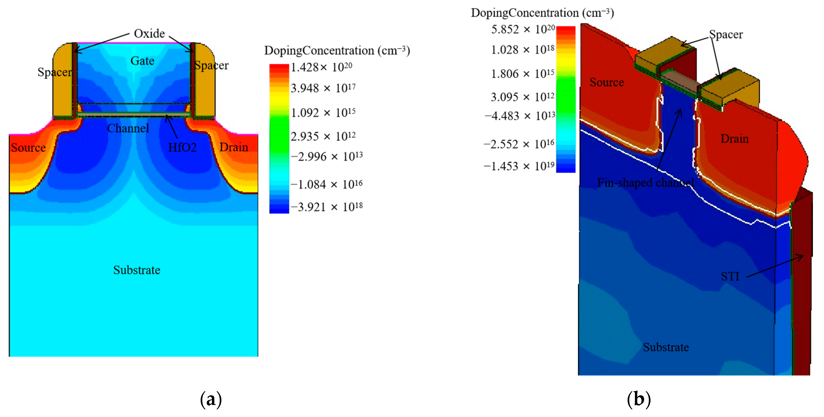
2. Experimental Setup
3. Simulation Results and Discussion
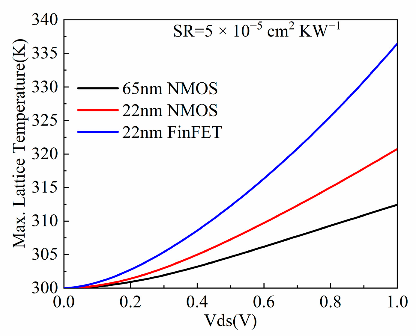
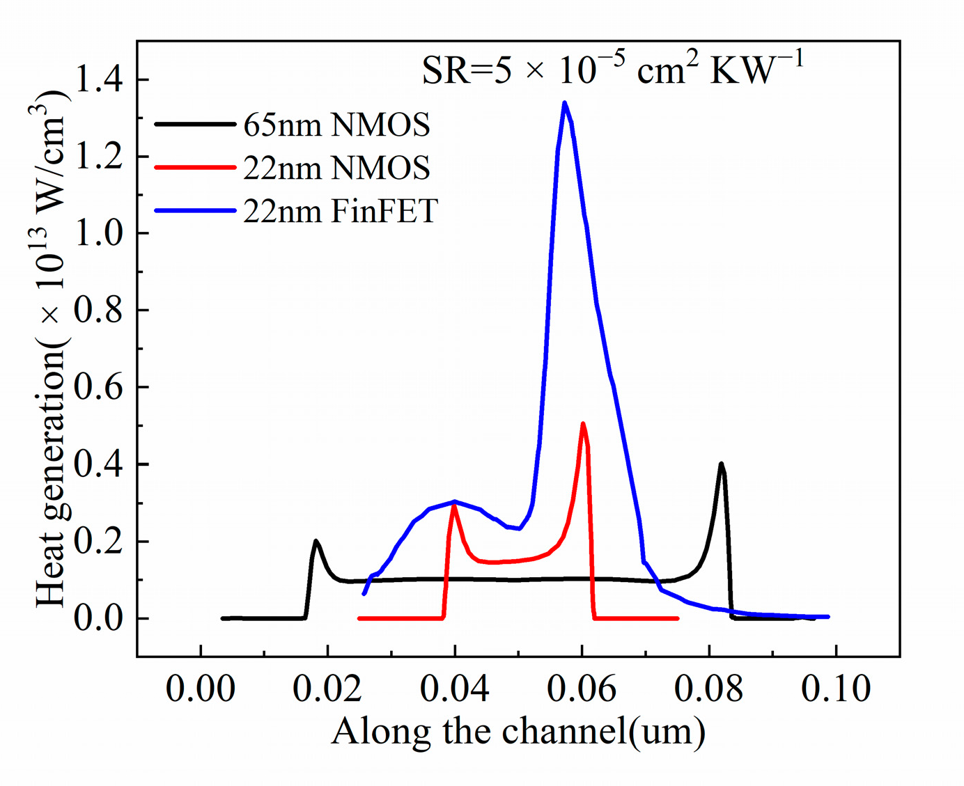
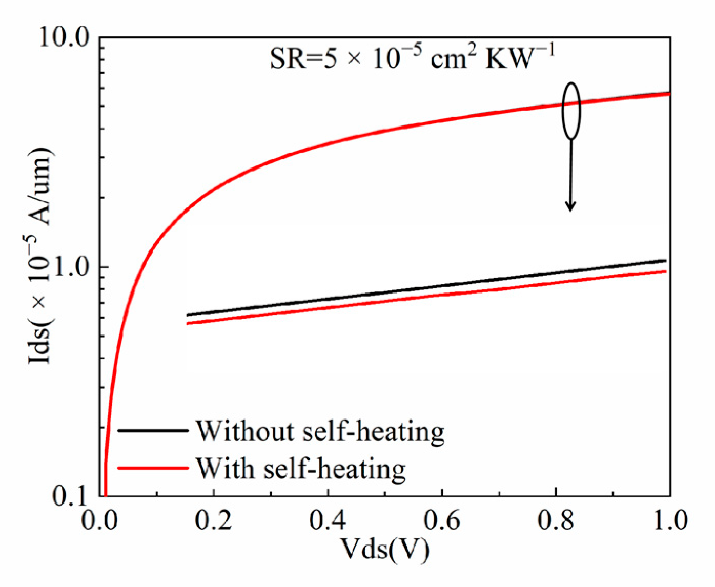
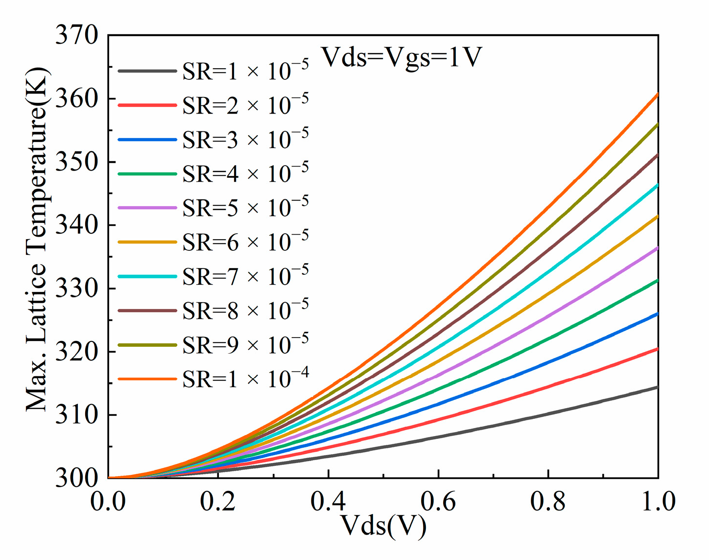
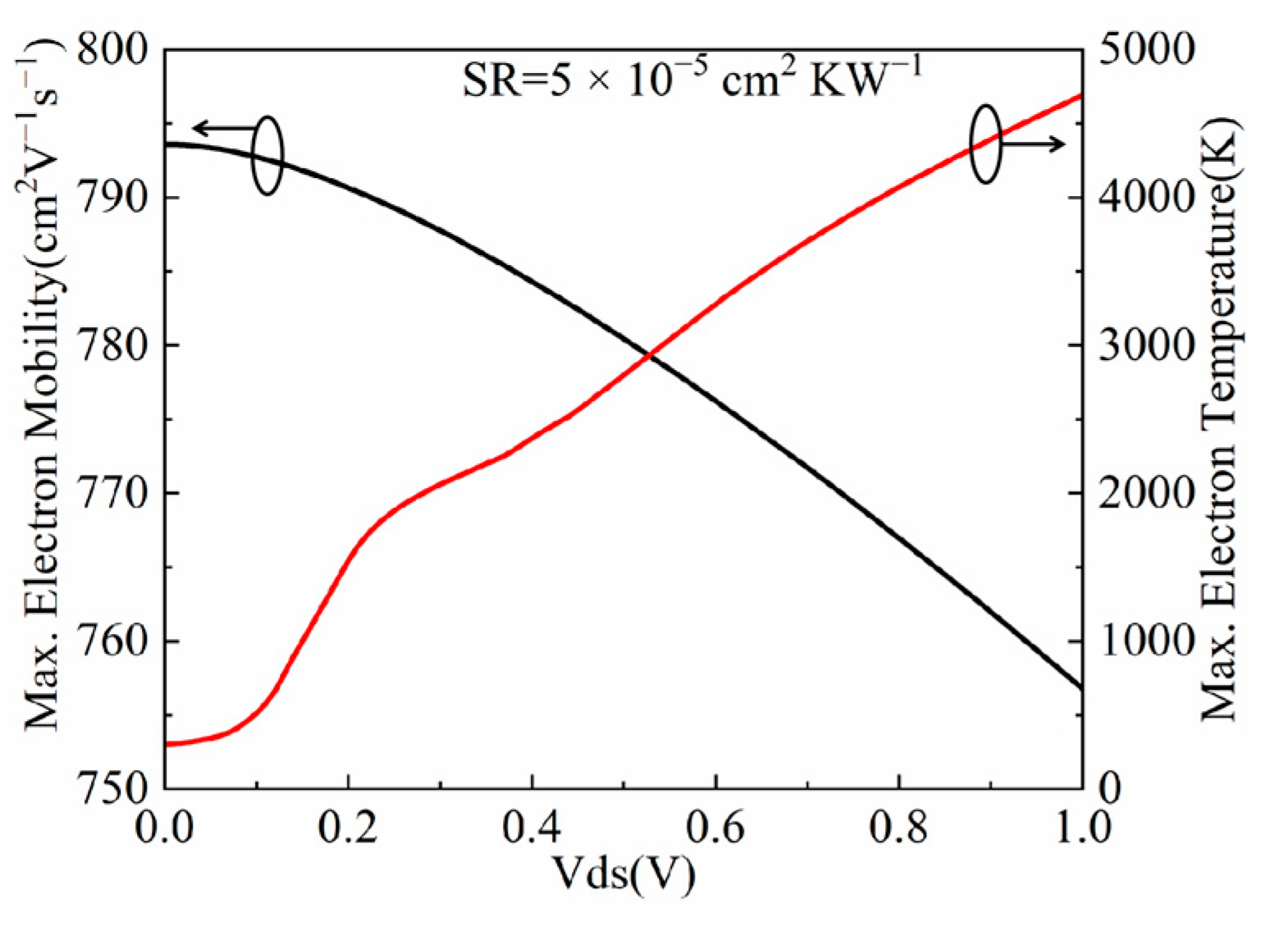
3.1. Performance Characteristics under the Self-Heating Effect
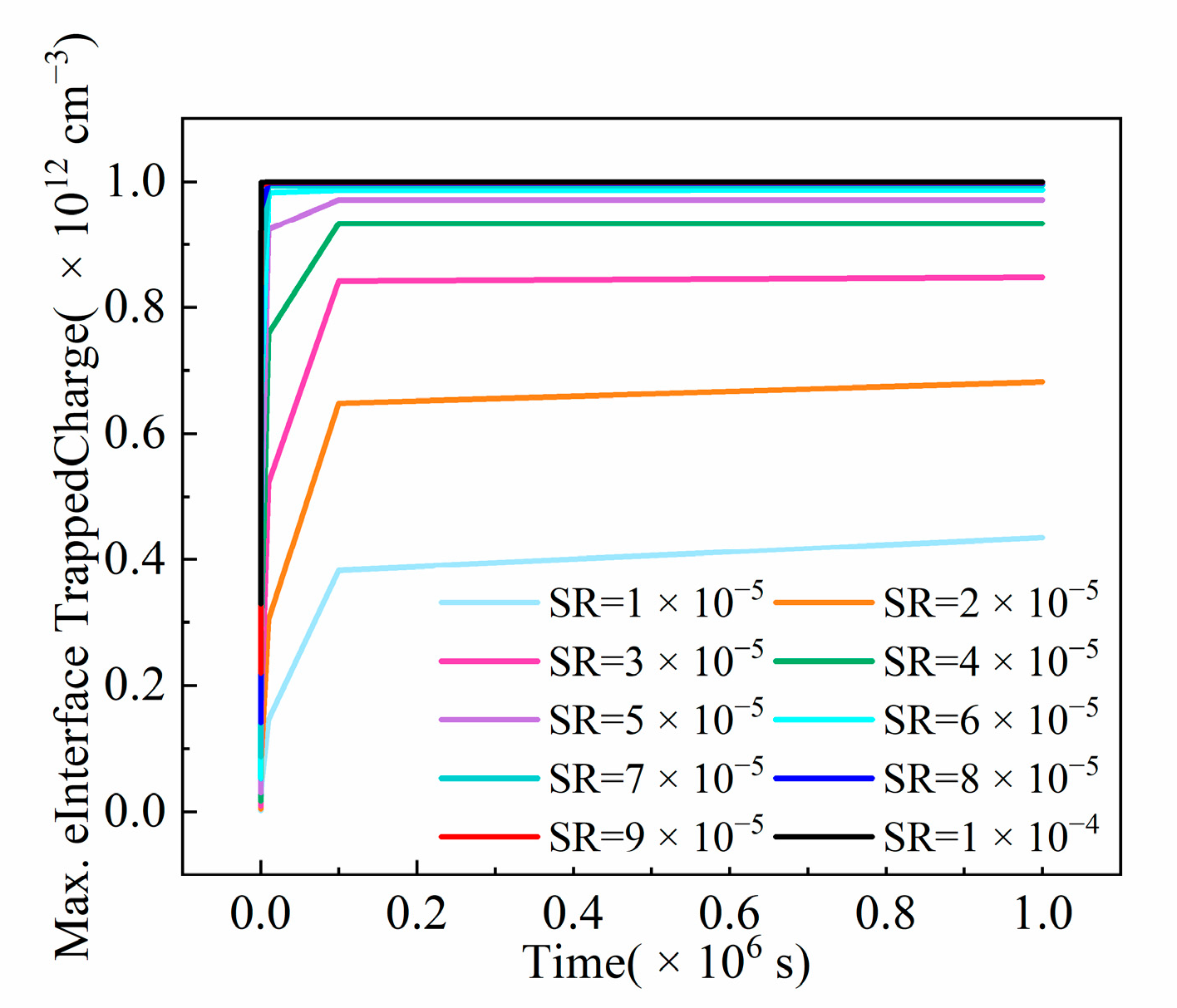
3.2. Performance Characteristics under HCI
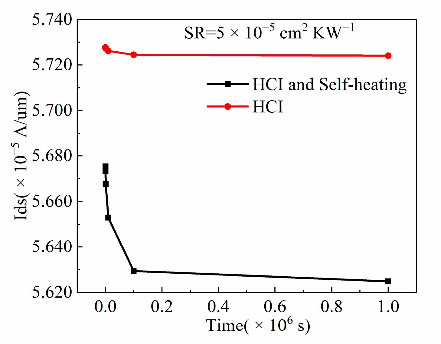
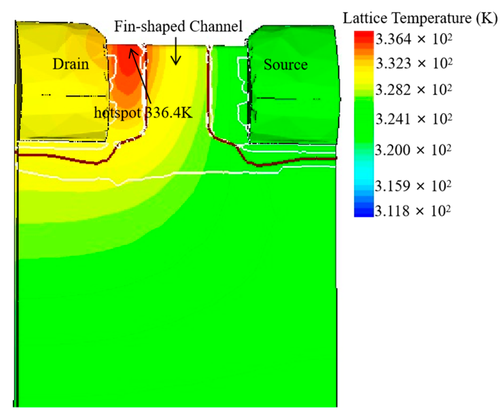
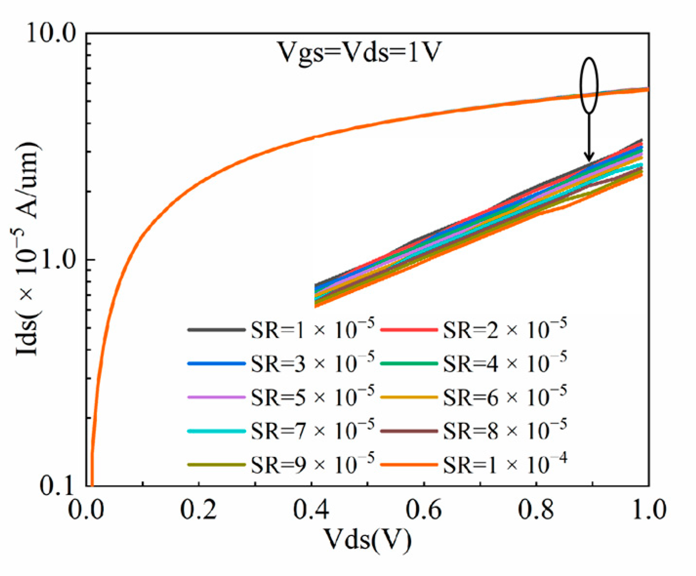
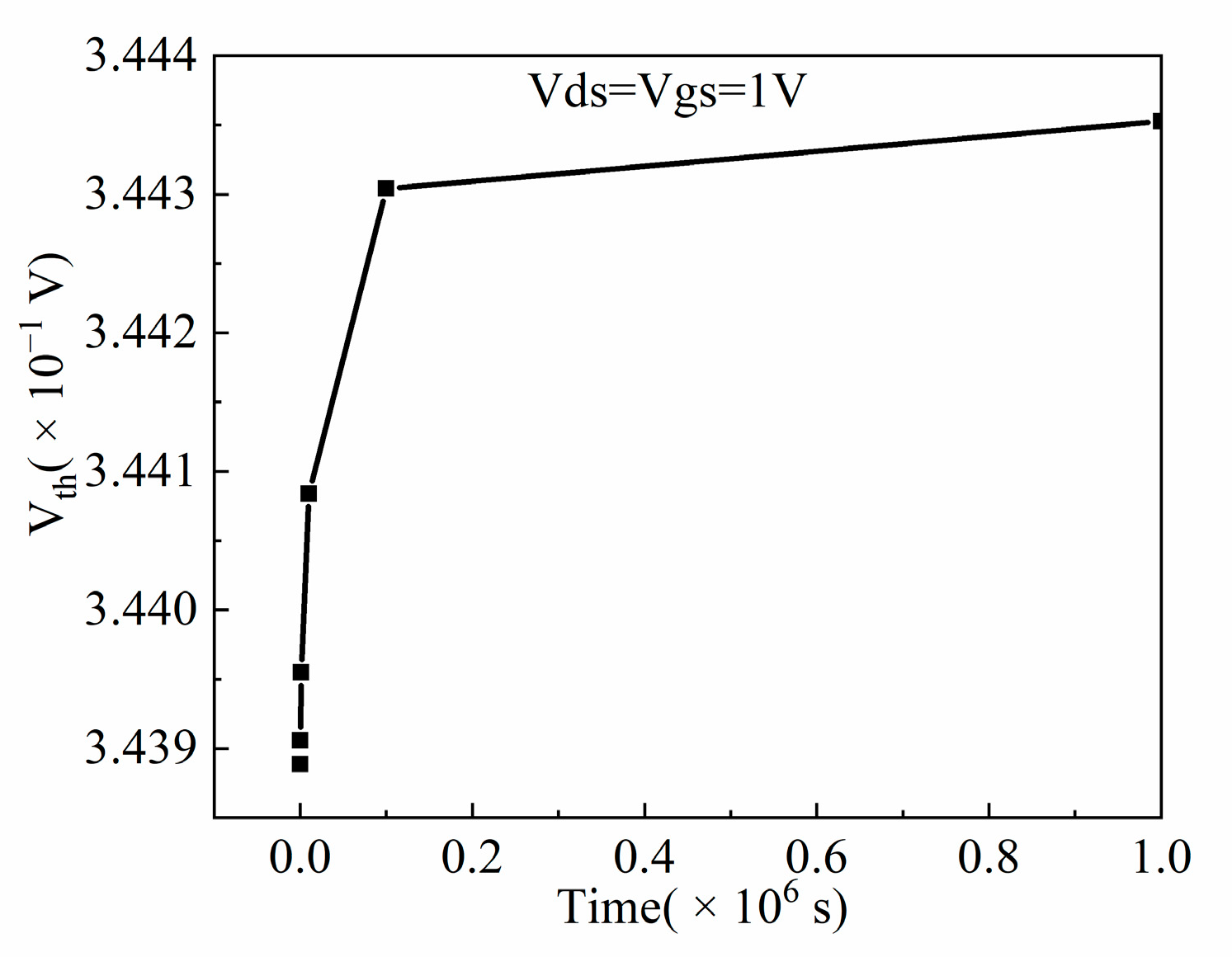
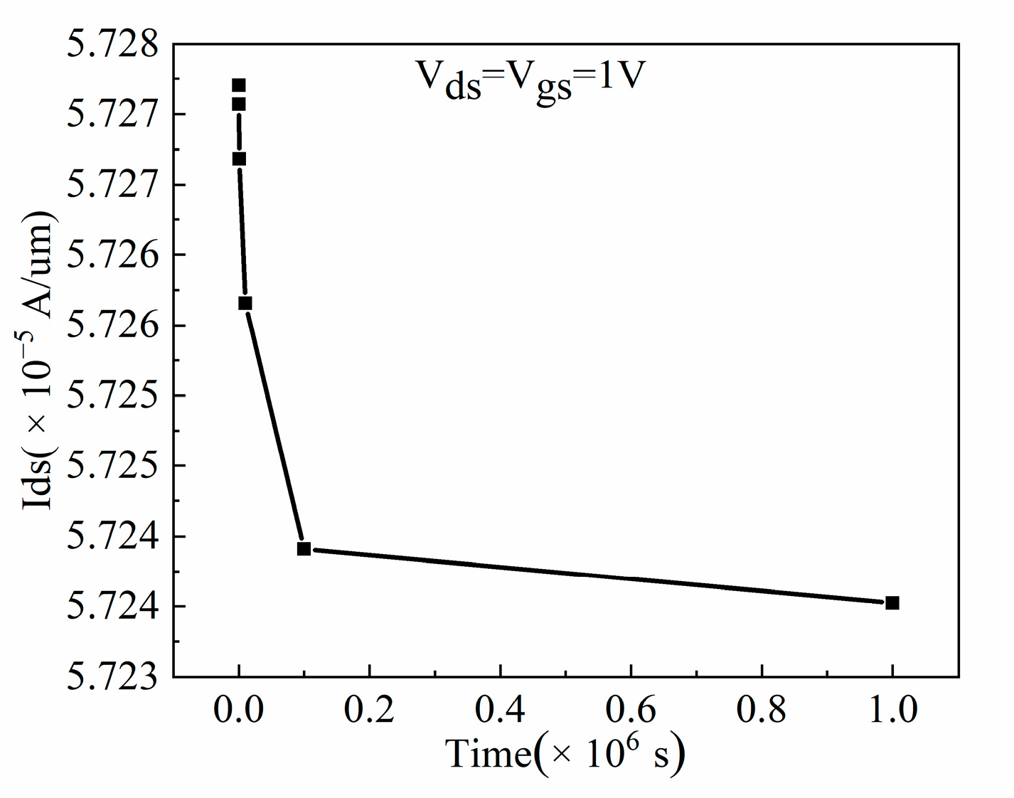
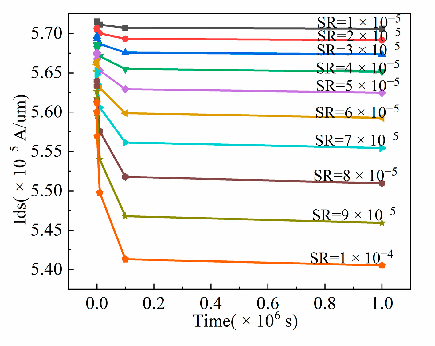
3.3. Performance Characteristics under the Self-Heating Effect and HCI
4. Conclusions
Author Contributions
Funding
Data Availability Statement
Conflicts of Interest
Abbreviations
| HCI | Hot Carrier Injection |
| SR | Surface Resistance |
| FinFET | Fin-shape Field Effect Transistor |
| NFinFET | N-channel FinFET |
| NMOS | N-channel MOSFET |
| STI | Shallow Trench Isolation |
References
- Liao, M.H.; Hsieh, C.P.; Lee, C.C. Systematic investigation of self-heating effect on CMOS logic transistors from 20 to 5nm technology nodes by experimental thermoelectric measurements and finite element modeling. IEEE Trans. Electron Devices 2017, 64, 646–648. [Google Scholar] [CrossRef]
- Prasad, C. A review of self-heating effects in advanced CMOS Technologies. IEEE Trans. Electron Devices 2019, 66, 4546–4555. [Google Scholar] [CrossRef]
- Purwar, V.; Gupta, R.; Tiwari, P.K.; Dubey, S. Investigating the Impact of Self-Heating Effects on some Thermal and Electrical Characteristics of Dielectric Pocket Gate-all-around (DPGAA) MOSFETs. Silicon 2021, 14, 7053–7063. [Google Scholar] [CrossRef]
- Steven, M.; Fernando, G. Self-heating and its implications on hot carrier reliability evaluations. In Proceedings of the 2015 IEEE International Reliability Physics Symposium, Monterey, CA, USA, 19–23 April 2015; pp. 4A.4.1–4A.4.6. [Google Scholar]
- Takacs, D.; Trager, J. Temperature increase by self-hcating in VLSI CMOS. In Proceedings of the ESSDERC’87: 17th European Solid State Device Research Conference, Bologna, Italy, 14–17 September 1987; pp. 729–732. [Google Scholar]
- Mautry, P.G.; Trager, J. Self-heating and temperature measurement in sub-um-MOSFETs. In Proceedings of the ESSDERC’89: 19th European Solid State Device Research Conference, Berlin, Germany, 11–14 September 1989; pp. 675–678. [Google Scholar]
- Petrosyants, K.O.; Orekhov, E.; Kharitonov, I.; Popov, D.A.; Dmitri, A.; Orlikovsky, A.A. TCAD analysis of self-heating effects in bulk silicon and SOI n-MOSFETs. In Proceedings of the International Conference Micro-and Nano-Electronics 2012, Zvenigorod, Russian, 1–5 October 2012; SPIE: Bellingham, WA, USA, 2013. [Google Scholar]
- Petrosyants, K.O.; Popov, D.A. Simulating the self-heating effect for MOSFETs with various configurations of buried oxide. Russ. Microelectron. 2019, 48, 467–469. [Google Scholar] [CrossRef]
- Catoggio, E.; Guerrieri, S.D.; Bonani, F. Efficient TCAD thermal analysis of semiconductor devices. IEEE Trans. Electron Devices 2021, 68, 5462–5468. [Google Scholar] [CrossRef]
- Su, Y.L.; Lai, J.H.; Sun, L. Investigation of self-heating effects in vacuum gate dielectric gate-all-around vertically stacked silicon nanowire field effect transistors. IEEE Trans. Electron Devices 2020, 67, 4085–4091. [Google Scholar] [CrossRef]
- Jeon, J.; Jhon, H.S.; Kang, M. Circuit modeling of the electro-thermal behavior of nanoscale bulk-FinFETs. J. Comput. Electron. 2017, 17, 146–152. [Google Scholar] [CrossRef]
- Kumar, A.; Srinivas, P.S.T.N.; Tiwari, P.K. An insight into self-heating effects and its implications on hot carrier degradation for silicon-nanotube-based double gate-all-around(DGAA) MOSFETs. IEEE J. Electron Devi. 2019, 7, 1100–1108. [Google Scholar] [CrossRef]
- Yang, F.Y.; Dalcanale, S.; Gajda, M.; Karboyan, S.; Uren, M.J.; Kuball, M. The impact of hot electrons and self-heating during hard-switching in AlGaN/GaN HEMTs. IEEE Trans. Electron Devices 2020, 67, 869–874. [Google Scholar] [CrossRef]
- Thingujam, T.; Son, D.H.; Kim, J.G.; Cristoloveanu, S.; Lee, J.H. Effects of interface traps and self-heating on the performance of GAA GaN Vertical. IEEE Trans. Electron Devices 2020, 67, 816–821. [Google Scholar] [CrossRef]
- Kumar, U.S.; Rao, V.R. A thermal-aware device design considerations for nanoscale SOI and bulk FinFETs. IEEE Trans. Electron Devices 2016, 63, 280–287. [Google Scholar] [CrossRef]
- Dai, J.R.; Liu, S.Y.; Zhang, C.W.; Sun, C.C.; Sun, W.F. SPICE modeling for hot carrier effect of MOSFET device. J. Southeast Univ. 2015, 45, 12–16. [Google Scholar]
- Prabowo, B.A.; Amethystna, S.K.; Tsai, J.R.; Yang, S.M.; Sheu, G. Interface trap distribution for HCI reliability assessment on bend gate structure by 3D TCAD simulation. In Proceedings of the 2012 19th IEEE International Symposium on the Physical and Failure Analysis of Integrated Circuits, Singapore, 2–6 July 2012. [Google Scholar]
- Penzin, O.; Haggag, A.; Mcmahon, W.; Lyumkis, E.; Hess, K. MOSFET degradation kinetics and its simulation. IEEE Trans. Electron Devices 2003, 50, 1445–1450. [Google Scholar] [CrossRef]
- Ruch, B.; Pobegen, G.; Grassser, T. Localizing hot-carrier degradation in Silicon trench MOSFETs. IEEE Trans. Electron Devices 2021, 68, 1804–1809. [Google Scholar] [CrossRef]
- Couso, C.; Martin-Martinez, J.; Porti, M.; Nafria, M.; Aymerich, X. Efficient methodology to extract interface traps parameters for TCAD simulations. Microelectron. Eng. 2017, 178, 66–70. [Google Scholar] [CrossRef]
- Son, D.; Jeon, S.; Kang, M.; Shin, H. 3D TCAD analysis of hot-carrier degradation mechanisms in 10nm node input/output bulk FinFETs. J. Semicond. Technol. Sci. 2016, 16, 191–197. [Google Scholar] [CrossRef]
- Ren, Z.X.; Xia, A.; Wang, J.N.; Zhang, X.; Huang, R. Impact of TID radiation on hot-carrier effects in 65nm bulk Si NMOSFETs. In Proceedings of the 2018 China Semiconductor Technology International Conference (CSTIC), Shanghai, China, 11–12 March 2018; pp. 1–3. [Google Scholar]
- Synopsys, Inc. Sentaurus Device User Guide, Version N-2017.09; Synopsys: Mountain View, CA, USA, 2016. [Google Scholar]
- Yu, L.T.; Ren, J.G.; Lu, X.; Wang, X.X. NBTI and HCI Aging prediction and reliability screening during production test. IEEE Trans. Comput.-Aided Des. Integr. Circuits Syst. 2020, 39, 3000–3011. [Google Scholar] [CrossRef]
- Wang, B.S.; Cui, J.W.; Guo, Q.; Zheng, Q.W.; Wei, Y.; Xi, S.X. The influence of total ionizing dose on the hot carrier injection of 22 nm bulk nFinFET. J. Semicond. 2020, 41, 122102–122107. [Google Scholar] [CrossRef]
- Gao, L.; Liu, Y.; Yu, Y.Q. Correlation Analysis of TID and HCI Effect on Nanoscale MOS Devices; Xidian University: Xian, China, 2015. [Google Scholar]
- Jeong, M.K.; Lee, J.H. Mobility and effective electric field in nonplanar channel MOSFETs. IEEE Trans. Nanotechnol. 2008, 8, 106–110. [Google Scholar] [CrossRef]
- Swahn, B.; Hassoun, S. Electro-thermal analysis of multi-fin devices. IEEE Trans. Very Large Scale Integr. VLSI Syst. 2008, 16, 816–829. [Google Scholar] [CrossRef]


| Parameter | Symbol | Value |
|---|---|---|
| Channel length (nm) | L | 65, 22 |
| Gate oxide thickness (nm) | Tox | 0.6 |
| High-k oxide thickness (nm) | THf | 20 |
| Souce/Drain junction depth (nm) | Xj | 40 |
| Souce/Drain extension junction depth (nm) | Xjs | 8 |
| Halo pocket depth (nm) | XjHalo | 50 |
| Halo pocket concentration (cm−3) | NHalo | 4 × 10¹⁸ |
| Souce/Drain concentration (cm−3) | NS/D | 1.5 × 10²⁰ |
| Souce/Drain extension concentration (cm−3) | NExtension | 1 × 10¹⁹ |
| Substrate concentration (cm−3) | Nsub | 5 × 10¹⁵ |
| Surface Resistance (cm2 KW−1) | SR | 1 × 10⁻⁵–1 × 10⁻⁴ |
| Drain to source voltage (V) | Vds | 0–1 |
| Gate to source voltage (V) | Vgs | 0–1 |
| Parameter | Symbol | Value |
|---|---|---|
| Channel length (nm) | L | 22 |
| Gate oxide thickness (nm) | Tox | 1 |
| High-k oxide thickness (nm) | THf | 2 |
| Fin Height (nm) | HFin | 40 |
| Fin Width (nm) | WFin | 17 |
| Souce/Drain concentration (cm−3) | NS/D | 5 × 10¹⁵ |
| Substrate concentration (cm−3) | Nsub | 1 × 10¹⁵ |
| Surface Resistance (cm2 KW−1) | SR | 1 × 10⁻⁵–1 × 10⁻⁴ |
| Drain to source voltage (V) | Vds | 0–1 |
| Gate to source voltage (V) | Vgs | 0–1 |
| Material | Thermal Conductivity (WK−1 cm−1) |
|---|---|
| SiO2 | 0.014 |
| Si (bulk) | 1.48 |
| Si (Fin) | 0.13 |
| Poly Si | 1.5 |
| HfO2 | 0.023 |
| Si3N4 | 0.185 |
| TiN | 0.192 |
| SR (cm2 KW−1) | Time (s) | Total Heat (W) | Electric Power (W) |
|---|---|---|---|
| 1 × 10⁻⁵ | 10 | 5.46388 × 10⁻⁵ | 5.71516813464 × 10⁻⁵ |
| 100 | 5.463616 × 10⁻⁵ | 5.71481694648 × 10⁻⁵ | |
| 1000 | 5.463014 × 10⁻⁵ | 5.71384276547 × 10⁻⁵ | |
| 10,000 | 5.46018 × 10⁻⁵ | 5.71127985774 × 10⁻⁵ | |
| 100,000 | 5.455764 × 10⁻⁵ | 5.70695061607 × 10⁻⁵ | |
| 1,000,000 | 5.454896 × 10⁻⁵ | 5.70600452826 × 10⁻⁵ | |
| 2 × 10⁻⁵ | 10 | 5.466508 × 10⁻⁵ | 5.70651366756 × 10⁻⁵ |
| 100 | 5.466068 × 10⁻⁵ | 5.70593219536 × 10⁻⁵ | |
| 1000 | 5.464068 × 10⁻⁵ | 5.70432883455 × 10⁻⁵ | |
| 10,000 | 5.461038 × 10⁻⁵ | 5.70012833352 × 10⁻⁵ | |
| 100,000 | 5.453421 × 10⁻⁵ | 5.69307354766 × 10⁻⁵ | |
| 1,000,000 | 5.452013 × 10⁻⁵ | 5.69155432188 × 10⁻⁵ | |
| 3 × 10⁻⁵ | 10 | 5.466111 × 10⁻⁵ | 5.69675211279 × 10⁻⁵ |
| 100 | 5.465413 × 10⁻⁵ | 5.6958350135 × 10⁻⁵ | |
| 1000 | 5.46283 × 10⁻⁵ | 5.69331548613 × 10⁻⁵ | |
| 10,000 | 5.45705 × 10⁻⁵ | 5.68673603157 × 10⁻⁵ | |
| 100,000 | 5.446274 × 10⁻⁵ | 5.67580419574 × 10⁻⁵ | |
| 1,000,000 | 5.443128 × 10⁻⁵ | 5.67351230947 × 10⁻⁵ | |
| 4 × 10⁻⁵ | 10 | 5.463975 × 10⁻⁵ | 5.68634327628 × 10⁻⁵ |
| 100 | 5.461902 × 10⁻⁵ | 5.6849418515 × 10⁻⁵ | |
| 1000 | 5.459479 × 10⁻⁵ | 5.68110640842 × 10⁻⁵ | |
| 10,000 | 5.450186 × 10⁻⁵ | 5.67114134919 × 10⁻⁵ | |
| 100,000 | 5.432998 × 10⁻⁵ | 5.6548435426 × 10⁻⁵ | |
| 1,000,000 | 5.429868 × 10⁻⁵ | 5.65152385571 × 10⁻⁵ | |
| 5 × 10⁻⁵ | 10 | 5.459634 × 10⁻⁵ | 5.6753961365 × 10⁻⁵ |
| 100 | 5.460443 × 10⁻⁵ | 5.67330566528 × 10⁻⁵ | |
| 1000 | 5.453399 × 10⁻⁵ | 5.6676030086 × 10⁻⁵ | |
| 10,000 | 5.439573 × 10⁻⁵ | 5.65291425804 × 10⁻⁵ | |
| 100,000 | 5.415387 × 10⁻⁵ | 5.62936626834 × 10⁻⁵ | |
| 1,000,000 | 5.410054 × 10⁻⁵ | 5.62481972882 × 10⁻⁵ | |
| 6 × 10⁻⁵ | 10 | 5.455347 × 10⁻⁵ | 5.66394452119 × 10⁻⁵ |
| 100 | 5.451982 × 10⁻⁵ | 5.66088826268 × 10⁻⁵ | |
| 1000 | 5.444668 × 10⁻⁵ | 5.65258175509 × 10⁻⁵ | |
| 10,000 | 5.424986 × 10⁻⁵ | 5.63144653359 × 10⁻⁵ | |
| 100,000 | 5.391934 × 10⁻⁵ | 5.59850969861 × 10⁻⁵ | |
| 1,000,000 | 5.385224 × 10⁻⁵ | 5.59258497826 × 10⁻⁵ | |
| 7 × 10⁻⁵ | 10 | 5.449223 × 10⁻⁵ | 5.65197687632 × 10⁻⁵ |
| 100 | 5.444807 × 10⁻⁵ | 5.64758360032 × 10⁻⁵ | |
| 1000 | 5.435171 × 10⁻⁵ | 5.63571430317 × 10⁻⁵ | |
| 10,000 | 5.40695 × 10⁻⁵ | 5.6059792514 × 10⁻⁵ | |
| 100,000 | 5.362063 × 10⁻⁵ | 5.56146013132 × 10⁻⁵ | |
| 1,000,000 | 5.353012 × 10⁻⁵ | 5.55423612409 × 10⁻⁵ | |
| 8 × 10⁻⁵ | 10 | 5.4423 × 10⁻⁵ | 5.63945236534 × 10⁻⁵ |
| 100 | 5.436438 × 10⁻⁵ | 5.63323025709 × 10⁻⁵ | |
| 1000 | 5.422656 × 10⁻⁵ | 5.61657278472 × 10⁻⁵ | |
| 10,000 | 5.383865 × 10⁻⁵ | 5.57567909814 × 10⁻⁵ | |
| 100,000 | 5.324494 × 10⁻⁵ | 5.51782929022 × 10⁻⁵ | |
| 1,000,000 | 5.315336 × 10⁻⁵ | 5.509621932 × 10⁻⁵ | |
| 9 × 10⁻⁵ | 10 | 5.434621 × 10⁻⁵ | 5.62629974705 × 10⁻⁵ |
| 100 | 5.425804 × 10⁻⁵ | 5.61761841972 × 10⁻⁵ | |
| 1000 | 5.406845 × 10⁻⁵ | 5.59465483844 × 10⁻⁵ | |
| 10,000 | 5.355166 × 10⁻⁵ | 5.53977980035 × 10⁻⁵ | |
| 100,000 | 5.281394 × 10⁻⁵ | 5.46793156284 × 10⁻⁵ | |
| 1,000,000 | 5.270793 × 10⁻⁵ | 5.45942119901 × 10⁻⁵ | |
| 1 × 10⁻⁴ | 10 | 5.426152 × 10⁻⁵ | 5.61241803495 × 10⁻⁵ |
| 100 | 5.414727 × 10⁻⁵ | 5.60047540938 × 10⁻⁵ | |
| 1000 | 5.388327 × 10⁻⁵ | 5.56935774279 × 10⁻⁵ | |
| 10,000 | 5.320421 × 10⁻⁵ | 5.49777477636 × 10⁻⁵ | |
| 100,000 | 5.231724 × 10⁻⁵ | 5.412926789 × 10⁻⁵ | |
| 1,000,000 | 5.222591 × 10⁻⁵ | 5.40506290857 × 10⁻⁵ |
Publisher’s Note: MDPI stays neutral with regard to jurisdictional claims in published maps and institutional affiliations. |
© 2022 by the authors. Licensee MDPI, Basel, Switzerland. This article is an open access article distributed under the terms and conditions of the Creative Commons Attribution (CC BY) license (https://creativecommons.org/licenses/by/4.0/).
Share and Cite
Liu, Y.; Ma, Y.; Yu, Z.; Lou, S.; Qu, Y.; Chang, Y. An Investigation into the Comprehensive Impact of Self-Heating and Hot Carrier Injection. Electronics 2022, 11, 2753. https://doi.org/10.3390/electronics11172753
Liu Y, Ma Y, Yu Z, Lou S, Qu Y, Chang Y. An Investigation into the Comprehensive Impact of Self-Heating and Hot Carrier Injection. Electronics. 2022; 11(17):2753. https://doi.org/10.3390/electronics11172753
Chicago/Turabian StyleLiu, Yan, Yanhua Ma, Zhaojie Yu, Shanshan Lou, Yang Qu, and Yuchun Chang. 2022. "An Investigation into the Comprehensive Impact of Self-Heating and Hot Carrier Injection" Electronics 11, no. 17: 2753. https://doi.org/10.3390/electronics11172753
APA StyleLiu, Y., Ma, Y., Yu, Z., Lou, S., Qu, Y., & Chang, Y. (2022). An Investigation into the Comprehensive Impact of Self-Heating and Hot Carrier Injection. Electronics, 11(17), 2753. https://doi.org/10.3390/electronics11172753