
CONNA: Configurable Matrix Multiplication Engine for Neural Network Acceleration


Abstract
:1. Introduction
2. Background and Related Works
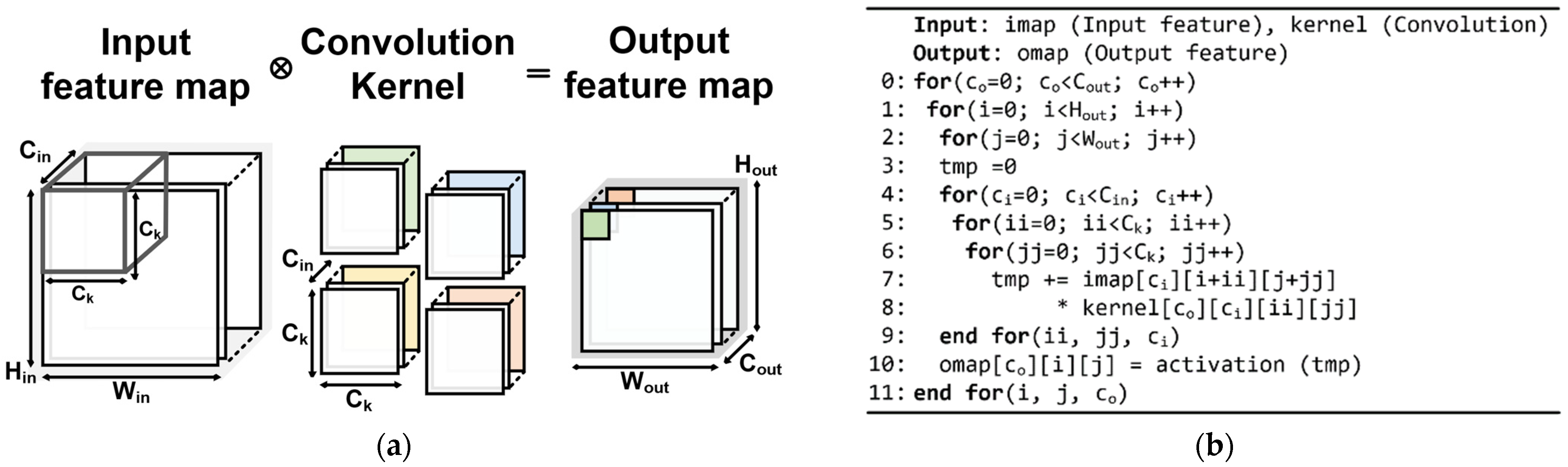
2.1. Convolutional Neural Network
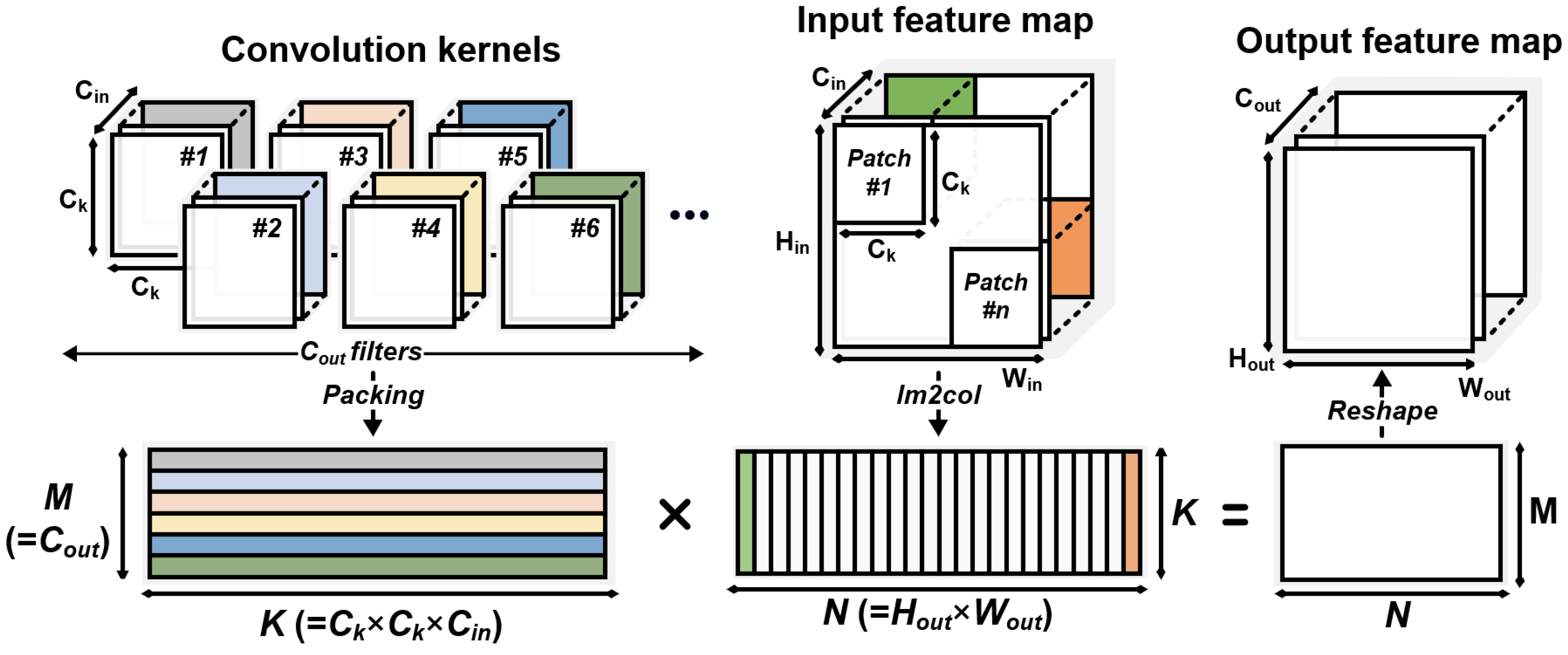
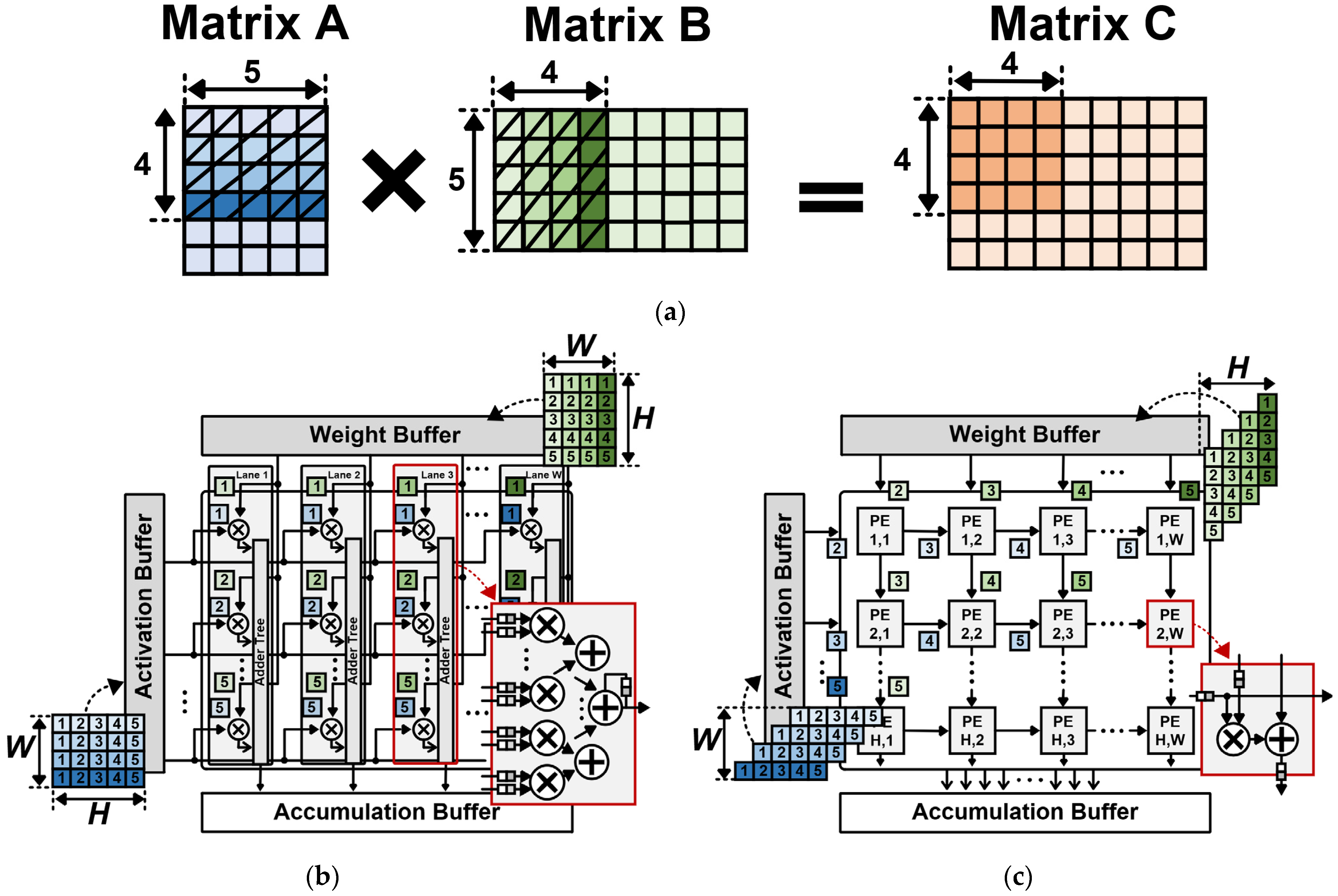
2.2. Matrix Multiplication
2.3. Accelerating CNN on Neural Processing Unit
2.4. Handling Various Shapes and Dimensions of Matrix Multiplication in NPU
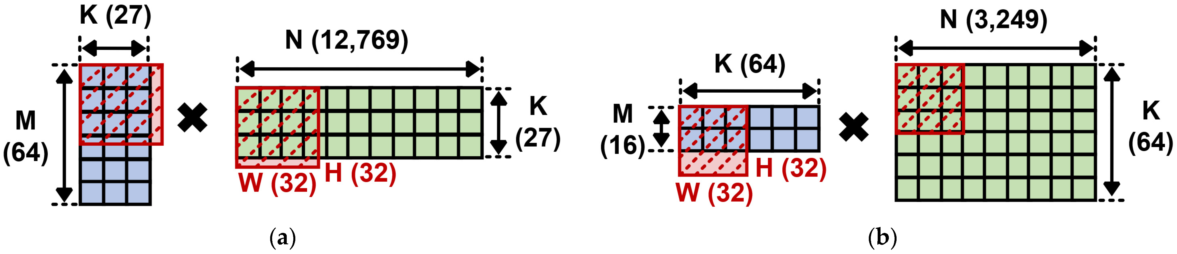
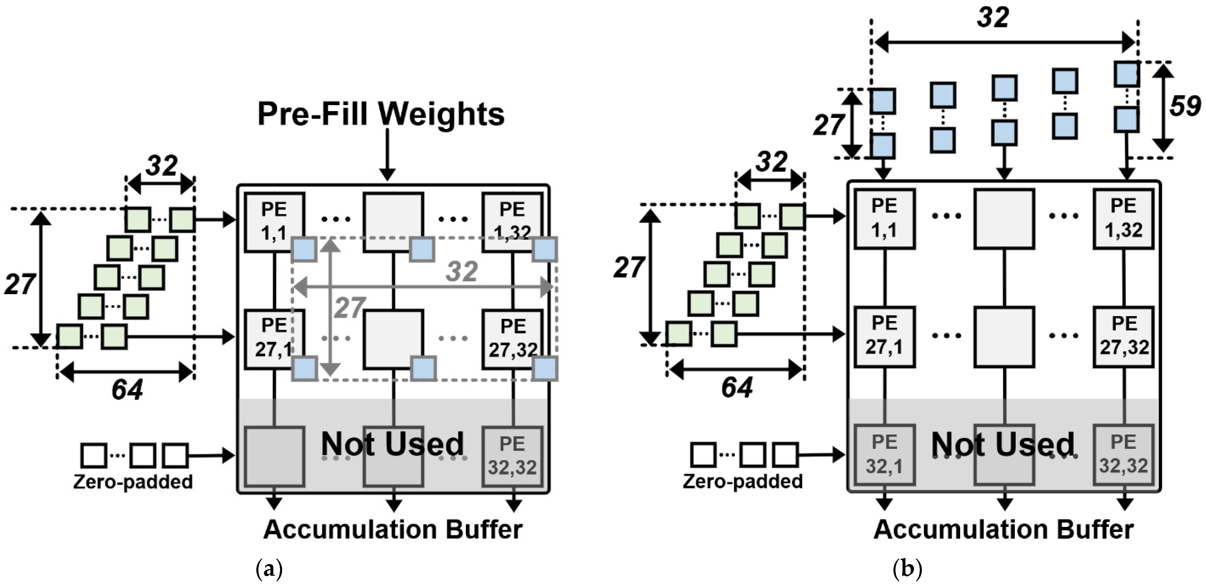
2.4.1. Computing Unit Utilization
2.4.2. Latency and Throughput
3. CONNA Architecture
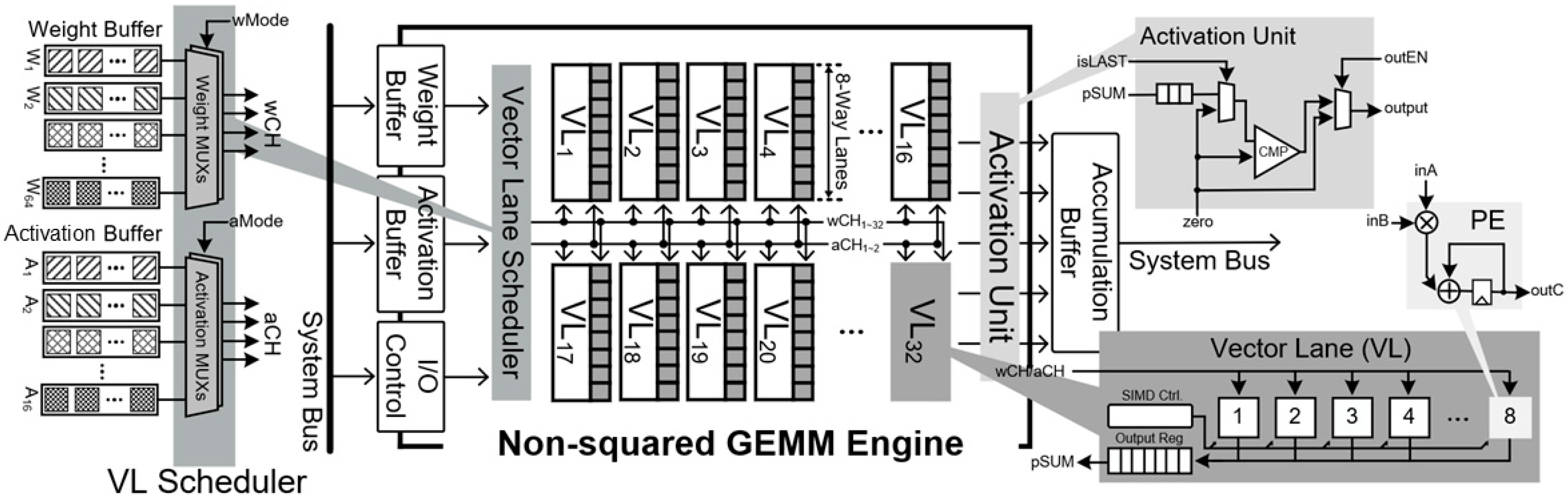
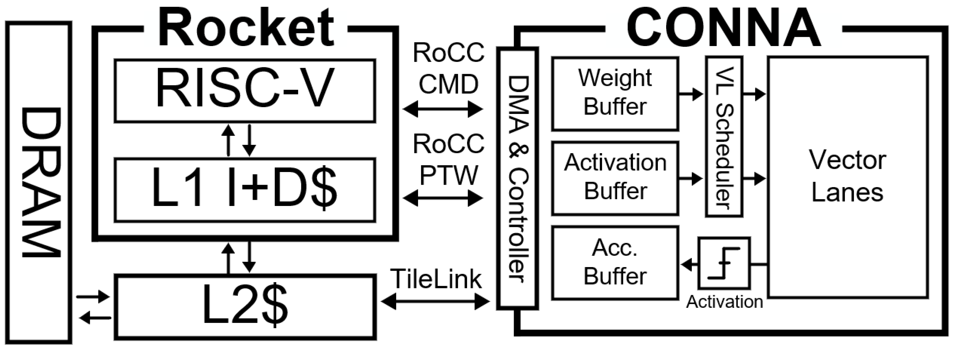
3.1. Architecture Overview
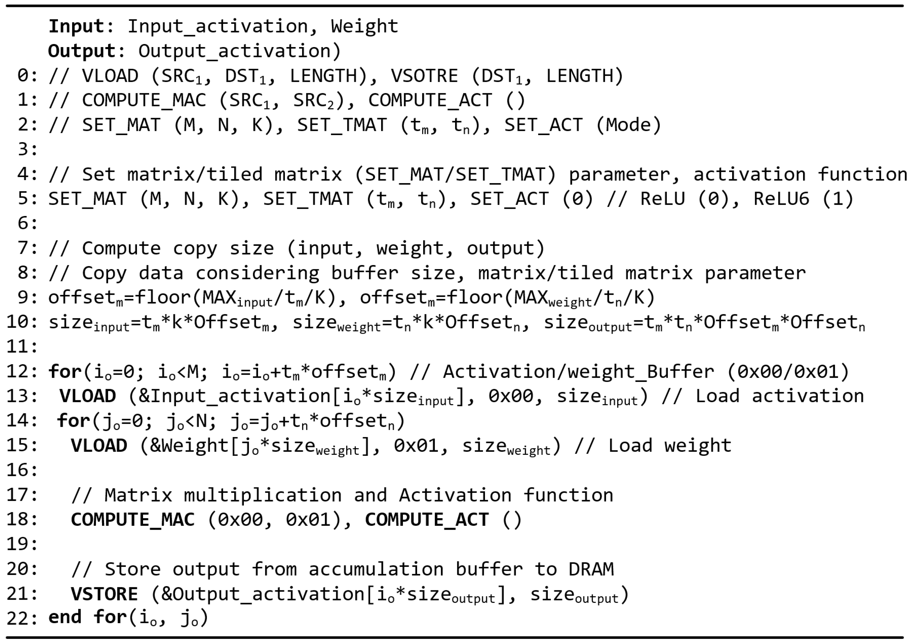
3.2. Proposed Configurable Matrix Engine
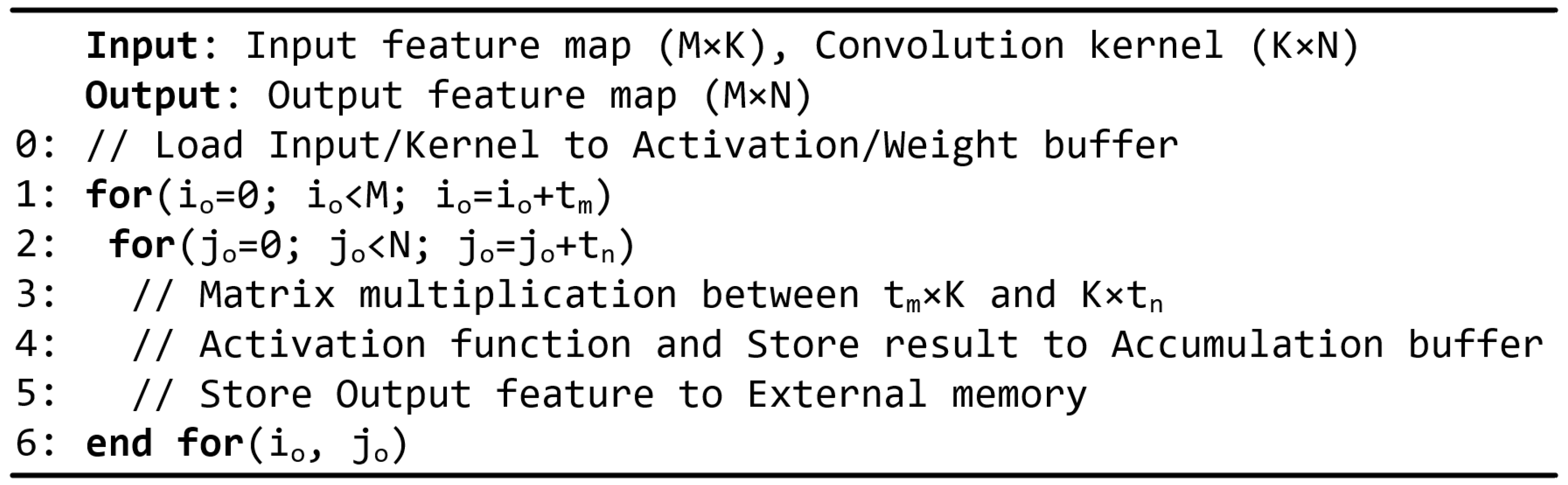
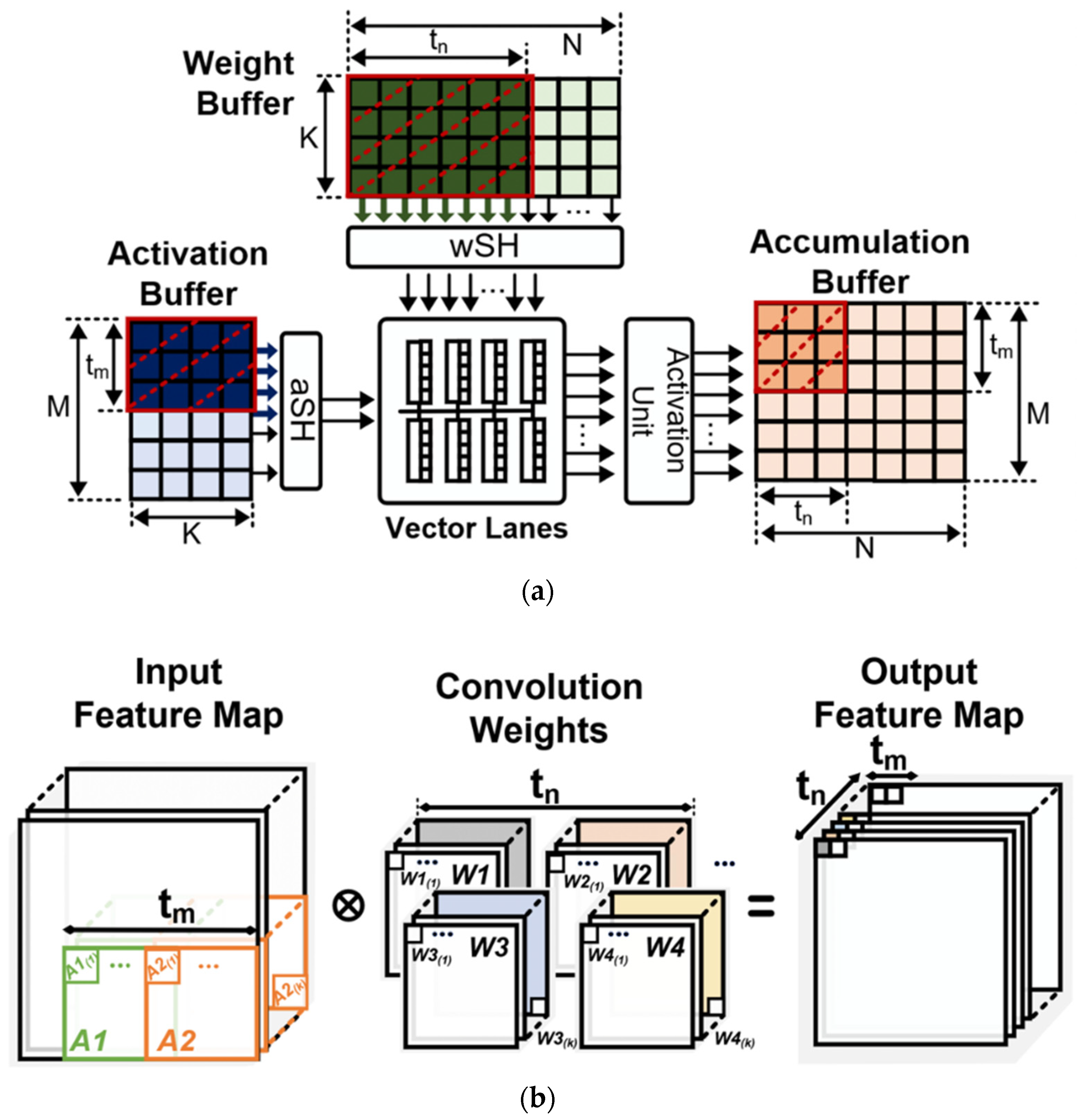
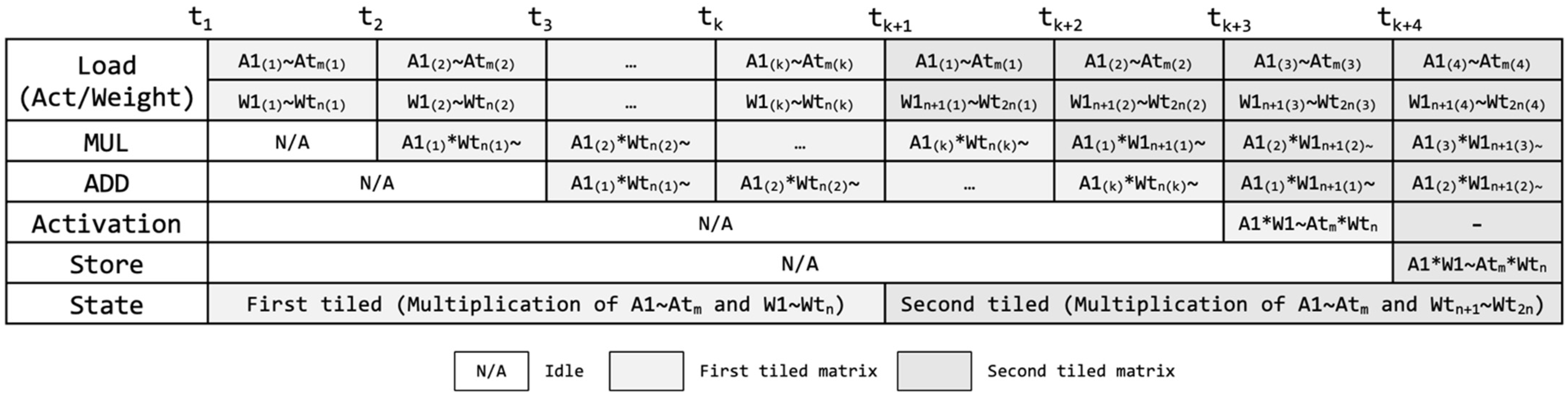
3.3. Convolution Operation inside CONNA
4. Hardware Implementation
4.1. CONNA Implmentation
4.2. Integration of CONNA and RISC-V MCU
5. Evaluation
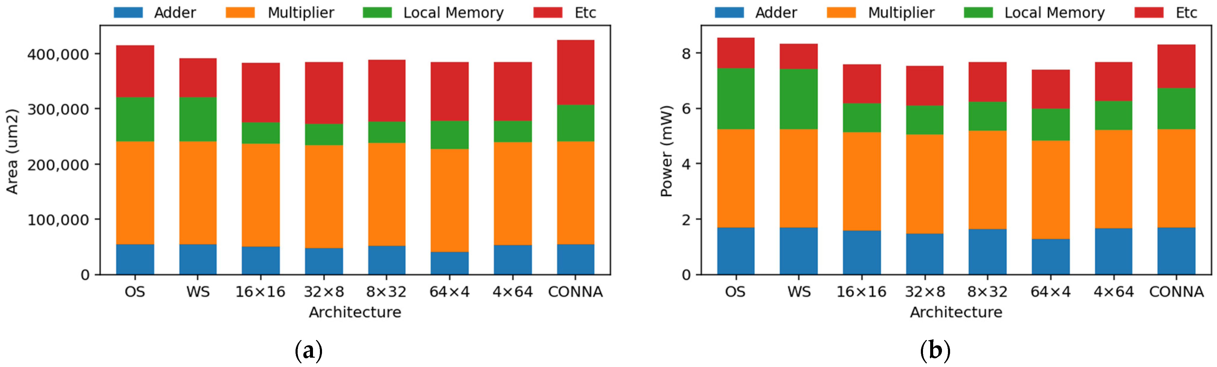
5.1. Computing Unit Utilization of CONNA
5.2. Latency and Throughput of CONNA
5.3. Comparision with the State-of-the-Art Accelerators
5.3.1. SIMD-Based Accelerators
5.3.2. SA-Based Accelerators
6. Discussion
7. Conclusions
Author Contributions
Funding
Acknowledgments
Conflicts of Interest
References
- Girshick, R.; Donahue, J.; Darrell, T.; Malik, J. Rich feature hierarchies for accurate object detection and semantic segmentation. In Proceedings of the IEEE Conference on Computer Vision and Pattern Recognition (ECCV), Zurich, Switzerland, 6–12 September 2014. [Google Scholar]
- Farhadi, A.; Redmon, J. Yolov3: An incremental improvement. In Proceedings of the Computer Vision and Pattern Recognition (CVPR), Salt Lake City, UT, USA, 18–22 June 2018. [Google Scholar]
- Zhao, Q.; Sheng, T.; Wang, Y.; Tang, Z.; Chen, Y.; Cai, L.; Ling, H. M2det: A single-shot object detector based on multi-level feature pyramid network. In Proceedings of the AAAI Conference on Artificial Intelligence, Honolulu, HI, USA, 27 January–1 February 2019. [Google Scholar]
- Iandola, F.N.; Han, S.; Moskewicz, M.W.; Ashraf, K.; Dally, W.J.; Keutzer, K. SqueezeNet: AlexNet-level accuracy with 50x fewer parameters and <0.5 MB model size. In Proceedings of the International Conference on Learning Representations (ICLR), Toulon, France, 24–26 April 2017. [Google Scholar]
- Tan, M.; Le, Q. Efficientnet: Rethinking model scaling for convolutional neural networks. In Proceedings of the International Conference on Machine Learning (ICML), Long Beach, CA, USA, 9–15 June 2019. [Google Scholar]
- He, K.; Zhang, X.; Ren, S.; Sun, J. Deep residual learning for image recognition. In Proceedings of the IEEE Conference on Computer Vision and Pattern Recognition (CVPR), Las Vegas, NV, USA, 26 June–1 July 2016. [Google Scholar]
- Karpathy, A.; Toderici, G.; Shetty, S.; Leung, T.; Sukthankar, R.; Fei-Fei, L. Large-scale video classification with convolutional neural networks. In Proceedings of the IEEE Conference on Computer Vision and Pattern Recognition (CVPR), Stockholm, Sweden, 24–28 August 2014. [Google Scholar]
- Guo, D.; Zhou, W.; Li, H.; Wang, M. Hierarchical LSTM for sign language translation. In Proceedings of the AAAI Conference on Artificial Intelligence, New Orleans, LA, USA, 2–7 February 2018. [Google Scholar]
- Devlin, J.; Chang, M.W.; Lee, K.; Toutanova, K. Bert: Pre-training of deep bidirectional transformers for language understanding. In Proceedings of the Conference of the North American Chapter of the Association for Computational Linguistics: Human Language Technologies (NAACL-HLT), Minneapolis, MN, USA, 2–7 June 2019. [Google Scholar]
- Ogden, S.S.; Guo, T. Characterizing the deep neural networks inference performance of mobile applications. arXiv 2019, arXiv:1909.04783. [Google Scholar]
- Cong, J.; Xiao, B. Minimizing computation in convolutional neural networks. In Proceedings of the International Conference on Artificial Neural Networks (ICANN), Hamburg, Germany, 15–19 September 2014. [Google Scholar]
- Lavin, A.; Gray, S. Fast algorithms for convolutional neural networks. In Proceedings of the IEEE Conference on Computer Vision and Pattern Recognition (CVPR), Las Vegas, NV, USA, 27–30 June 2016. [Google Scholar]
- Strobel, K.; Zhu, S.; Chang, R.; Koppula, S. Accurate, low-latency visual perception for autonomous racing: Challenges, mechanisms, and practical solutions. In Proceedings of the IEEE/RSJ International Conference on Intelligent Robots and Systems (IROS), Las Vegas, NV, USA, 25–29 October 2020. [Google Scholar]
- Kim, Y.D.; Park, E.; Yoo, S.; Choi, T.; Yang, L.; Shin, D. Compression of deep convolutional neural networks for fast and low power mobile applications. In Proceedings of the International Conference on Learning Representations (ICLR), San Juan, PR, USA, 2–4 May 2016. [Google Scholar]
- Aguilera, C.A.; Aguilera, C.; Navarro, C.A.; Sappa, A.D. Fast CNN Stereo Depth Estimation through Embedded GPU Devices. Sensors 2020, 20, 3249. [Google Scholar] [CrossRef] [PubMed]
- NVDIA Deep Learning Accelerator. 2021. Available online: https://nvldla.org (accessed on 28 June 2022).
- Jouppi, N.P.; Young, C.; Patil, N.; Patterson, D.; Agrawal, G.; Bajwa, R.; Yoon, D.H. In-datacenter performance analysis of a tensor processing unit. In Proceedings of the International Symposium on Computer Architecture (ISCA), Toronto, ON, Canada, 24–28 June 2017. [Google Scholar]
- Genc, H.; Kim, S.; Amid, A.; Haj-Ali, A.; Iyer, V.; Prakash, P.; Zhao, J.; Grubb, D.; Liew, H.; Mao, H.; et al. Gemmini: Enabling systematic deep-learning architecture evaluation via full-stack integration. In Proceedings of the Design Automation Conference (DAC), San Francisco, CA, USA, 7–10 December 2021. [Google Scholar]
- Guo, K.; Sui, L.; Qiu, J.; Yu, J.; Wang, J.; Yao, S.; Yang, H. Angel-eye: A complete design flow for mapping CNN onto embedded FPGA. IEEE Trans. Comput.-Aided Des. Integr. Circuits Syst. 2017, 37, 35–47. [Google Scholar] [CrossRef]
- Chen, Y.-H.; Emer, J.; Sze, V. Eyeriss: A spatial architecture for energy-efficient dataflow for convolutional neural networks. In Proceedings of the International Symposium on Computer Architecture (ISCA), Seoul, Korea, 18–22 June 2016. [Google Scholar]
- Yue, J.; Liu, Y.; Yuan, Z.; Wang, Z.; Guo, Q.; Li, J.; Yang, H. A 3.77 TOPS/W convolutional neural network processor with priority-driven kernel optimization. IEEE Trans. Circuits Syst. 2018, 66, 277–281. [Google Scholar]
- Chong, Y.S.; Goh, W.L.; Ong, Y.S.; Nambiar, V.P.; Do, A.T. An Energy-efficient Convolution Unit for Depthwise Separable Convolutional Neural Networks. In Proceedings of the International Symposium on Circuits and Systems (ISCAS), Virtual, 23–26 May 2021. [Google Scholar]
- Qin, E.; Samajdar, A.; Kwon, H.; Nadella, V.; Srinivasan, S.; Das, D.; Krishna, T. Sigma: A sparse and irregular gemm accelerator with flexible interconnects for DNN training. In Proceedings of the IEEE International Symposium on High Performance Computer Architecture (HPCA), San Diego, CA, USA, 22–26 February 2020. [Google Scholar]
- Kwon, H.; Samajdar, A.; Krishna, T. Maeri: Enabling flexible dataflow mapping over dnn accelerators via reconfigurable interconnects. In ACM SIGPLAN Notices; Association for Computing Machinery: New York, NY, USA, 2018; pp. 461–475. [Google Scholar]
- Wang, S.; Zhou, D.; Han, X.; Yoshimura, T. Chain-NN: An energy-efficient 1D chain architecture for accelerating deep convolutional neural networks. arXiv 2017, arXiv:1703.01457. [Google Scholar]
- Selvam, S.; Ganesan, V.; Kumar, P. Fuseconv: Fully separable convolutions for fast inference on systolic arrays. In Proceedings of the Design, Automation & Test in Europe Conference & Exhibition (DATE), Virtual, 14–23 March 2022. [Google Scholar]
- Anderson, A.; Gregg, D. Optimal DNN primitive selection with partitioned boolean quadratic programming. In Proceedings of the 2018 International Symposium on Code Generation and Optimization (CGO), New York, NY, USA, 24–28 February 2018. [Google Scholar]
- Anderson, A.; Vasudevan, A.; Keane, C.; Gregg, D. Low-memory gemm-based convolution algorithms for deep neural networks. arXiv 2017, arXiv:1709.03395. [Google Scholar]
- Abadi, M.; Barham, P.; Chen, J.; Chen, Z.; Davis, A.; Dean, J.; Devin, M.; Ghemawat, S.; Irving, G.; Isard, M.; et al. Tensorflow: A system for large-scale machine learning. In Proceedings of the USENIX Symposium on Operating Systems Design and Implementation (OSDI), Savannah, GA, USA, 2–4 November 2016. [Google Scholar]
- Paszke, A.; Gross, S.; Massa, F.; Lerer, A.; Bradbury, J.; Chanan, G.; Chintala, S. Pytorch: An imperative style, high-performance deep learning library. arXiv 2019, arXiv:1912.01703. [Google Scholar]
- Chen, J.; Xiong, N.; Liang, X.; Tao, D.; Li, S.; Ouyang, K.; Chen, Z. TSM2: Optimizing tall-and-skinny matrix-matrix multiplication on GPUs. In Proceedings of the ACM International Conference on Supercomputing (ICS), Phoenix, AZ, USA, 26–28 June 2019. [Google Scholar]
- Mitra, G.; Johnston, B.; Rendell, A.P.; McCreath, E.; Zhou, J. Use of SIMD vector operations to accelerate application code performance on low-powered ARM and Intel platforms. In Proceedings of the International Symposium on Parallel & Distributed Processing (IPDPS), Chicago, IL, USA, 23–27 May 2016. [Google Scholar]
- Stephens, N.; Biles, S.; Boettcher, M.; Eapen, J.; Eyole, M.; Gabrielli, G.; Walker, P. The ARM scalable vector extension. IEEE Micro 2018, 37, 26–39. [Google Scholar] [CrossRef] [Green Version]
- Lee, W.J.; Shin, Y.; Lee, J.; Kim, J.W.; Nah, J.H.; Jung, S.; Lee, S.; Park, H.S.; Han, T.D. SGRT: A mobile GPU architecture for real-time ray tracing. In Proceedings of the High-Performance Graphics Conference (HPG), Anaheim, CA, USA, 19–21 July 2013. [Google Scholar]
- Kang, H.J. Accelerator-aware pruning for convolutional neural networks. IEEE Trans. Circuits Syst. Video Technol. 2019, 30, 2093–2103. [Google Scholar] [CrossRef] [Green Version]
- Bachrach, J.; Vo, H.; Richards, B.; Lee, Y.; Waterman, A.; Avižienis, R.; Asanović, K. Chisel: Constructing hardware in a scala embedded language. In Proceedings of the Design Automation Conference (DAC), San Francisco, CA, USA, 3–7 June 2012. [Google Scholar]
- Asanovic, K.; Avizienis, R.; Bachrach, J.; Beamer, S.; Biancolin, D.; Celio, C.; Waterman, A. The Rocket Chip Generator; Tech. Rep. UCB/EECS-2016-17; EECS Department, University of California: Berkeley, CA, USA, 2016. [Google Scholar]
- Balasubramonian, R.; Kahng, A.B.; Muralimanohar, N.; Shafiee, A.; Srinivas, V. CACTI 7: New tools for interconnect exploration in innovative off-chip memories. ACM Trans. Archit. Code Optim. (TACO) 2017, 14, 1–25. [Google Scholar] [CrossRef]
- Cook, H.; Terpstra, W.; Lee, Y. Diplomatic design patterns: A TileLink case study. In Proceedings of the Workshop on Computer Architecture Research with RISC-V (CARRV), Boston, MA, USA, 14 October 2017. [Google Scholar]
- SiFive U54. Available online: https://www.sifive.com/cores/u54 (accessed on 25 April 2022).
- Moons, B.; Verhelst, M. An energy-efficient precision-scalable ConvNet processor in 40-nm CMOS. IEEE J. Solid State Circuits 2016, 52, 903–914. [Google Scholar] [CrossRef]
- Gonzalezm, A.; Hong, A. A Chipyard Comparison of NVDLA and Gemmini. Berkely, CA, USA, Tech. Rep. EE, 2020, 290-2. Available online: https://charleshong3.github.io/projects/nvdla_v_gemmini.pdf (accessed on 28 June 2022).
- Nebullvm. Available online: https://github.com/nebuly-ai/nebullvm (accessed on 25 April 2022).


| Layer Type | Layer Name * (Module/Kernel) | Matrix Multiplication Parameter | ||
|---|---|---|---|---|
| M | N | K | ||
| Convolution | conv1 (3 × 3) | 64 | 12,769 | 27 |
| Convolution | fire2/squeeze1 × 1 | 16 | 3136 | 64 |
| Convolution | fire2/expand1 × 1 | 64 | 3136 | 64 |
| Convolution | fire2/expand3 × 3 | 64 | 3136 | 576 |
| Convolution | fire5/squeeze1 × 1 | 32 | 784 | 256 |
| Convolution | fire5/expand1 × 1 | 128 | 784 | 32 |
| Fully connected | conv10 | 1000 | 196 | 512 |
| Architecture | Type | Peak Perf. 1 | Utilization (%) 2 | Achieved Performance (GOPS) | ||||||
|---|---|---|---|---|---|---|---|---|---|---|
| Conv1 | Fire2 (S1, E1, E3) 3 | Conv1 | Fire2 (S1, E1, E3) 3 | |||||||
| KOP3 [21] | SIMD | 94.8GOPS | 98.5 | 6.8 | 10.9 | 88.7 | 93.38 | 6.48 | 10.37 | 84.24 |
| Angle-Eye [19] | SIMD | 188GOPS | 84.4 | 8.3 | 8.3 | 75 | 158.68 | 15.6 | 15.6 | 141.0 |
| TPU [17] | SA | 23TOPS | 37.1 | 4.7 | 8.9 | 30.5 | 8533 | 1090 | 2037 | 7024 |
| Gemmini [18] | SA | 512GOPS | 99.6 | 49.6 | 60.6 | 98.4 | 509.95 | 253.95 | 310.27 | 503.65 |
| Eyeriss [20] | SA | 84GOPS | 68.6 | 50.9 | 61.0 | 91.4 | 57.62 | 42.76 | 51.24 | 76.78 |
| Layer | # of MAC | Clock Cycles | Latency (µs) | Throughput (FPS) 1 |
|---|---|---|---|---|
| conv1 (3 × 3) | 44.13 M | 75,200 | 150.4 | 6648.9 |
| fire2/squeeze1 × 1 | 6.42 M | 18,424 | 36.85 | 27,137 |
| fire2/expand1 × 1 | 25.69 M | 37,632 | 75.26 | 13,287.3 |
| fire2/expand3 × 3 | 231.21 M | 338,688 | 677.38 | 1476.3 |
| fire5/squeeze1 × 1 | 12.85 M | 38,400 | 76.8 | 13,020.8 |
| fire5/expand1 × 1 | 6.42 M | 9400 | 18.8 | 53,191.5 |
| fire5/expand3 × 3 | 57.8 M | 84,600 | 169.2 | 5910.2 |
| conv10 (fc) | 200.7 M | 336,896 | 673.79 | 1484.1 |
| Layer | Conv1 | Fire2/Squeeze1 × 1 | Fire2/Expand1 × 1 | Fire2/Expand3 × 3 |
|---|---|---|---|---|
| # of MAC | 44.13 M | 6.42 M | 25.69 M | 231.21 M |
| Latency (ms) | 0.95 | 1.98 | 4.95 | 5.49 |
| Throughput (FPS) | 1058.01 | 504.67 | 201.83 | 182.17 |
| Mode (tm × tn) | Activation (tm × N) | Weight (N × tn) |
|---|---|---|
| 1 (16 × 16) | 16 × N | N × 16 |
| 2 (8 × 32) | 8 × N | N × 32 |
| 3 (4 × 64) | 4 × N | N × 64 |
| 4 (64 × 4) | 64 × N | N × 4 |
| 5 (32 × 8) | 32 × N | N × 8 |
| Metric | Systolic Array (SA) | Single Instruction Multiple Data (SIMD) | CONNA | |||||
|---|---|---|---|---|---|---|---|---|
| OS | WS | 16 × 16 | 32 × 8 | 8 × 32 | 64 × 4 | 4 × 64 | ||
| MUL/ADD | 256/256 | 256/256 | 256/240 | 256/224 | 256/248 | 256/192 | 256/252 | 256/256 |
| Local Memory 1 | 12,288 b | 12,160 b | 2688 b | 3200 b | 2432 b | 4224 b | 2304 b | 8192 b |
| Peak GOPS | 102.4 | 102.4 | 99.2 | 96.0 | 100.8 | 89.6 | 101.6 | 102.4 |
| Real GOPS 2 | 52.37 | 59.77 | 75.54 | 64.76 | 69.03 | 50.51 | 69.58 | 84.88 |
| Area (mm2) | 2.334 | 2.312 | 2.303 | 2.304 | 2.308 | 2.304 | 2.304 | 2.344 |
| Power (mW) | 83.81 | 83.73 | 82.85 | 82.78 | 82.92 | 82.65 | 82.92 | 83.55 |
| Efficiency (TOPS/W) 3 | 624.9 | 713.8 | 911.8 | 782.3 | 832.5 | 611.1 | 839.1 | 1015.9 |
| Instruction | Instruction Type | Description |
|---|---|---|
| VLOAD | Data movement | Copy data from DRAM to CONNA |
| VSTORE | Data movement | Copy data from CONNA to DRAM |
| COMPUTE_MAT | Computation | Matrix multiplication |
| COMPUTE_ACT | Computation | Activation function |
| SET_MAT | Configuration | Set the matrix parameter |
| SET_TMAT | Configuration | Set the tiled matrix parameter |
| SET_ACT | Configuration | Set the activation function (ReLU/ReLU6) |
| Layer | Filter Shape (S1/E1/E3) 1 | Input Size (W × H × Cin) | # of OPS (Mega) | Matrix Multiplication Parameter 2 | ||
|---|---|---|---|---|---|---|
| M | N | K | ||||
| conv1 | 3 × 3 × 3 × 64 | 227 × 227 × 3 | 44.13 | 64 | 12,769 | 27 |
| fire2 | 16/64/64 | 57 × 57 × 64 | 6.7/6.7/59.9 | 16/64/64 | 3249 | 64/16/144 |
| fire3 | 16/64/64 | 57 × 57 × 128 | 13.3/6.7/59.9 | 16/64/64 | 3249 | 128/16/144 |
| fire4 | 32/128/128 | 29 × 29 × 256 | 6.9/6.9/62 | 32/128/128 | 841 | 128/32/288 |
| fire5 | 32/128/128 | 29 × 29 × 256 | 13.8/6.9/62 | 32/128/128 | 841 | 256/32/288 |
| fire6 | 48/192/192 | 15 × 15 × 384 | 5.5/4.1/37.3 | 48/192/192 | 225 | 256/48/432 |
| fire7 | 48/192/192 | 15 × 15 × 384 | 8.3/4.1/37.3 | 48/192/19 | 225 | 384/48/432 |
| fire8 | 64/256/256 | 15 × 15 × 512 | 11.1/7.4/66.4 | 64/256/256 | 225 | 384/64/576 |
| fire9 | 64/256/256 | 15 × 15 × 512 | 14.7/7.4/68.7 | 64/256/256 | 225 | 512/64/576 |
| conv10 | 1 × 1 × 512 × 1000 | 15 × 15 × 512 | 230.4 | 1000 | 225 | 512 |
| Total | 850.06 | |||||
| Architecture | Avg. Utilization | Cycles | Throughput 1 (FPS) | Efficiency 2 (FPS/W) |
|---|---|---|---|---|
| SIMD_16 × 16 | 95% | 2,250,587 | 88.9 | 1073.02 |
| SIMD_32 × 8 | 85% | 2,625,446 | 76.2 | 920.51 |
| SIMD_64 × 4 | 78% | 3,366,203 | 59.4 | 718.69 |
| SIMD_4 × 64 | 82% | 2,443,268 | 81.9 | 987.70 |
| SIMD_8 × 32 | 91% | 2,462,693 | 81.2 | 979.26 |
| OS | 52% | 3,246,212 | 61.6 | 735.0 |
| WS | 58% | 2,844,490 | 70.3 | 839.6 |
| CONNA | 98% | 2,002,956 | 100.0 | 1196.89 |
| Metrics | CPU | GPU | KOP3 | CONV 1 | MAERI | CONNA |
|---|---|---|---|---|---|---|
| Architecture | i3-6100U | Tesla T4 | SIMD_26 × 9 | SIMD_32 × 32 | SIMD_1 × 374 | CONNA |
| SRAM | 3 MB | 6.5 MB | 72 KB | 172 KB | 80 KB | 172 KB |
| Area (mm2) | 99 | 545 | 3.98 | 2.21 | 6.0 | 2.36 |
| Power (mW) | 1.5 × 10⁵ | 7 × 10⁵ | 72 | 71.61 | 520 | 83.55 |
| Tech. (nm) | 14 | 12 | 65 | 40 | 28 | 65 |
| Freq. (MHz) | 2.3 × 10³ | 1.6 × 10³ | 200 | 100 | 200 | 200 |
| MAC Unit (MUL/ADD) | 64/64 | 2560/2560 | 234/208 | 1024/1152 | 374/373 | 256/256 |
| Peak Perf. (GOPS) 2 | 130.9 | 1.3 × 10⁵ | 94.8 | 156 | 149.6 | 102.4 |
| Real Perf. (GOPS) 3 | 8.76 | 2.8 × 10³ | 58.05 | 51.07 | 128.7 | 84.88 |
| Throughput (FPS) | 10.3 | 3334 | 68.29 | 60.08 | 151.63 | 100 |
| Power Eff. | 0.7 | 47.63 | 987.47 | 838.99 * | 291.62 * | 1196.89 |
| Area Eff. | 0.1 | 6.12 | 17.16 | 27.19 ** | 25.27 ** | 42.37 |
| Overall Eff. | 0.0007 | 0.009 | 238.31 | 379.63 *** | 48.6 *** | 507.16 |
| Metrics | TPU | Eyeriss | Gemmini | Chain-NN | CONNA |
|---|---|---|---|---|---|
| Architecture | SA (WS) | SA (RS) | SA (OS) | SA (WS) | CONNA |
| SRAM | 28 MiB | 192 KB | 328 KB | 352 KB | 172 KB |
| Area (mm2) | 331 | 12.25 | 1.21 | 10.69 | 2.36 |
| Power (mW) | 8.6 × 10⁵ | 278 | 312.41 | 567.5 | 83.55 |
| Tech. (nm) | 28 | 65 | 16 | 28 | 65 |
| Freq. (MHz) | 700 | 200 | 500 | 700 | 200 |
| MAC Unit (MUL/ADD) | 65,536/65,536 | 168/168 | 1024/1024 | 576/576 | 256/256 |
| Peak Perf. (GOPS) | 92 × 104 | 84 | 256 | 806.4 | 102.4 |
| Real Perf. (GOPS) | 14.1 × 10⁴ | 43.03 | 54.4 | 604.43 | 84.88 |
| Throughput (FPS) | 1.6 × 10⁵ | 50.62 | 64 | 755.54 | 100 |
| Power Eff. | 221.9 * | 182.01 | 204.86 * | 1331.35 * | 1196.89 |
| Area Eff. | 501.86 ** | 4.13 | 52.89 ** | 70.68 ** | 42.37 |
| Overall Eff. | 6.69 *** | 14.86 | 169.31 *** | 124.54 *** | 507.16 |
Publisher’s Note: MDPI stays neutral with regard to jurisdictional claims in published maps and institutional affiliations. |
© 2022 by the authors. Licensee MDPI, Basel, Switzerland. This article is an open access article distributed under the terms and conditions of the Creative Commons Attribution (CC BY) license (https://creativecommons.org/licenses/by/4.0/).
Share and Cite
Park, S.-S.; Chung, K.-S. CONNA: Configurable Matrix Multiplication Engine for Neural Network Acceleration. Electronics 2022, 11, 2373. https://doi.org/10.3390/electronics11152373
Park S-S, Chung K-S. CONNA: Configurable Matrix Multiplication Engine for Neural Network Acceleration. Electronics. 2022; 11(15):2373. https://doi.org/10.3390/electronics11152373
Chicago/Turabian StylePark, Sang-Soo, and Ki-Seok Chung. 2022. "CONNA: Configurable Matrix Multiplication Engine for Neural Network Acceleration" Electronics 11, no. 15: 2373. https://doi.org/10.3390/electronics11152373
APA StylePark, S.-S., & Chung, K.-S. (2022). CONNA: Configurable Matrix Multiplication Engine for Neural Network Acceleration. Electronics, 11(15), 2373. https://doi.org/10.3390/electronics11152373