Article

Lightweight Architecture for Elliptic Curve Scalar Multiplication over Prime Field

1
School of Integrated Circuits and Electronics, Beijing Institute of Technology (BIT), Beijing 100081, China
2
BIT Chongqing Institute of Microelectronics and Microsystems, Chongqing 401332, China
3
UNISOC (Shanghai) Technology Co., Ltd., Shanghai 201203, China
4
BIT Chongqing Innovation Center, Chongqing 401135, China
*
Author to whom correspondence should be addressed.
Electronics 2022, 11(14), 2234; https://doi.org/10.3390/electronics11142234
Submission received: 14 June 2022 / Revised: 5 July 2022 / Accepted: 14 July 2022 / Published: 17 July 2022
(This article belongs to the Section Circuit and Signal Processing)

Abstract

:
In this paper, we present a novel lightweight elliptic curve scalar multiplication architecture for random Weierstrass curves over prime field F p . The elliptic curve scalar multiplication is executed in Jacobian coordinates based on the Montgomery ladder algorithm with (X,Y)-only common Z coordinate arithmetic. At the finite field operation level, the adder-based modular multiplier and modular divider are optimized by the pre-calculation method to reduce the critical path while maintaining low resource consumption. At the group operation level, the point addition and point doubling methods in (X,Y)-only common Z coordinate arithmetic are modified to improve computation parallelism. A compact scheduling method is presented to improve the architecture’s performance, which includes appropriate scheduling of finite field operations and specific register connections. Compared with existing works, our design is implemented on the FPGA platform without using DSPs or BRAMs for higher portability. It utilizes 6.4~6.5k slices in Kintex-7, Virtex-7, and ZYNQ FPGA and executes an elliptic curve scalar multiplication for a field size of 256-bit in 1.73 ms, 1.70 ms, and 1.80 ms, respectively. Additionally, our design is resistant to timing attacks, simple power analysis attacks, and safe-error attacks. This architecture outperforms most state-of-the-art lightweight designs in terms of area-time products.

1. Introduction

After the Diffie–Hellman key agreement was proposed, two widely used public-key cryptographies (asymmetric cryptography) are RSA cryptography proposed by Ron Rivest, Adi Shamir, and Leonard Adleman in 1978 [1] and elliptic curve cryptography (ECC) proposed by Koblitz [2] and Miller [3] in 1985. However, with the development of electronic information technology, the critical length of RSA is increasing to ensure security. In 2020, the recommendation proposed by the National Institute of Standards and Technology (NIST) [4] compared various cryptographic algorithm families based on the security level and it reports that an ECC cryptosystem requires a smaller key length than an RSA cryptosystem for the same security level. For example, a 256-bit ECC cryptosystem over a prime field can provide an equivalent security level to a 3072-bit RSA cryptosystem with lower resource consumption and computational latency [4,5]. Thus ECC is suitable for both high-speed real-time cryptographic applications and lightweight cryptographic applications such as blockchain technology and the Internet of Things (IoT). Generally, an ECC cryptosystem can be divided into four hierarchical layers: top protocol layer, elliptic curve scalar multiplication (ECSM) execution layer, group operation layer, and bottom finite field operation layer. The protocol layer is usually implemented using software to provide functions of cryptographic protocols such as elliptic curve digital signature algorithm (ECDSA), elliptic curve Diffie–Hellman (ECDH), etc. The other three layers constitute the ECSM architecture, which is the most complicated and crucial operation for an ECC cryptosystem.
To accelerate ECSM, many existing designs have been implemented on the field programmable gate arrays (FPGAs) and application-specific integrated circuits (ASICs) targeting ECC over prime fields. For example, a simple and effective technique in literature [6,7,8,9,10,11,12,13] utilizes the five specific primes recommended by the NIST, which significantly reduces the time and hardware resources cost of modular reduction. However, high-speed ECSM can be achieved using these special primes, but it limits the flexibility and generality. In realistic applications, a flexible ECC cryptosystem that supports multiple security protocol standards is necessary. On the other hand, some designs utilized the specific DSP blocks in the FPGA such as [7,9,12,13,14,15,16], which can accelerate multiplications without consuming logic resources. Nevertheless, these designs have low portability as they are difficult to rebuild on other FPGA platforms or ASICs.
The ECSM architecture in [16] supports generic curves, which are based on the double-and-add always method and utilize two bit-length adjustable Montgomery multipliers to perform ECSM. In 2016, Hossain et al. [11] developed an ECC processor based on both affine coordinates and mixed projective coordinates without using DSPs or BRAMs. Their design is implemented on both FPGA and ASIC platforms and supports two NIST recommended primes of F 224 and F 256 . The design in [17] utilizes four modular multipliers based on interleaved modular multiplication algorithm and radix-4 optimization technique to perform ECSM. It supports general curves over F p where p 256 and is resistant to simple power analysis attacks. Marzouqi et al. [12] took advantage of the redundant-signed-digit (RSD) technique to reduce the carry chain length of the adders used in their ECSM architecture. It is implemented on FPGA and supports only NIST recommended prime F 256 .
In 2021, Awaludin et al. [14] proposed a high-performance ECC processor over F 256 . It utilizes a novel Montgomery ladder algorithm presented by Hamburg [18] in 2020 and only takes 0.14 ms to perform a single ECSM, which is the fastest design in the literature for generic curves. Kudithi et al. [6] developed a ECSM architecture with 7.4k slices consumption in FPGA. Their design has fairly high performance compared to other lightweight ECC cryptosystems but only supports two NIST recommended primes. Hu et al. [19] proposed a low hardware consumption ECSM architecture that only uses LUT resources and supports all five NIST primes. In 2018, Shah et al. [20] proposed a high-speed RSD-based flexible ECC cryptosystem. Their design utilizes the Montgomery ladder with (X,Y)-only common Z coordinate (Co-Z) arithmetic to perform ECSM and adopts the RSD technique to optimize all the finite filed calculations. This design achieves a speed of 0.84 ms for a single ECSM operation without using DSP for acceleration.
On the other hand, some application contexts place higher demands on the hardware area and power consumption of the cryptosystem than the computation speed, such as the IoT [8]. The rise of IoT has sparked concerns about the security of data transmission between IoT devices. The ECC cryptosystem can solve the problems, but its complex calculation conflicts with the lightweight and flexible nature of IoT devices [21]. Fortunately, it is possible to reduce the throughput rate and the required computation speed of IoT by versatile access control methods [22]. Several ECSM architectures on the balance of hardware area and computational speed have been proposed for IoT devices. The designs in [23,24] utilize embedded ARM MCUs to execute ECSM, which allows their cryptosystems to have extremely low power consumption. However, the speed of software designs is not comparable to that of FPGAs or ASICs. In [8], an FPGA-based ECC processor architecture for IoT applications combines various lightweight modular methods and a classic binary ECSM method to achieve the trade-offs between speed and area. In 2021, Di Matteo improved the double-and-add always method and proposed a higher security ECC processor for IoT applications [25].
In general, most of the designs available in the literature for prime field ECSM architectures focus on improving the speed performance, resulting in a large circuit area. These designs are unfriendly to cryptosystems for small mobile devices that require a small area and low power consumption. Moreover, designs with low resource consumption generally have slow calculation speed or use DSPs at the expense of portability. In this paper, a lightweight ECSM architecture for random Weierstrass curves over a prime field is proposed. The major contributions are as follows:
  • An ECSM architecture based on four parallel modular multipliers and the Montgomery ladder with Co-Z arithmetic is implemented on FPGA using only 6.5k slices without DSPs or BRAMs. The modular multiplier and modular divider are optimized by the pre-calculation method to reduce the critical path while retaining a low resource consumption.
  • The point addition (PA) and point doubling (PD) methods in Co-Z arithmetic are modified to improve computation parallelism and accommodate four modular multipliers.
  • A compact scheduling method is proposed that includes appropriate scheduling of bottom finite field operations to reduce the clock cycles required and specific register connections to reduce the fan-out and path delay of the circuit.
  • The architecture is generic for random Weierstrass curves over a prime field and resistant to timing attacks, simple power analysis attacks, and safe-error attacks.
The rest of this paper is organized as follows: Section 2 provides a review of the mathematical background of ECC as well as several ECSM methods and attack methods. Section 3 presents all the technical details of our proposed ECSM architecture. Section 4 analyzes the resistance of our proposed ECSM architecture against side-channel attacks. The hardware architecture and implementation results, as well as comparisons with other similar designs, are presented in Section 5. Finally, Section 6 concludes the paper.

2. Preliminaries

2.1. Elliptic Curve Theory

Let E be an elliptic curve defined over a prime field F p with characteristic p 2 , 3 . The set of rational points on E is
E ( F p ) : = { ( x , y ) F p × F p | y 2 = x 3 + a x + b } { O } ,
where a , b F p with 16 ( 4 a 3 + 27 b 2 ) 0 , and O serving as its identity. According to the definition, the construction of a group requires that a particular set and the defined algorithm satisfy the group axiom. For the points set E ( F p ) of elliptic curves defined on the field F p , any two-point elements can be specially added according to the chord-and-tangent rule [26]. Together with this addition operation, the set of points E ( F p ) forms an abelian group. In standard plane affine coordinates, let P ( x 1 , y 1 ) and Q ( x 2 , y 2 ) F p , so R ( x 3 , y 3 ) = P + Q can be calculated as
x 3 = ( λ 2 x 1 x 2 ) mod p y 3 = [ λ ( x 1 x 3 ) y 1 ] mod p with λ = ( y 2 y 1 ) ( x 2 x 1 ) mod p , P Q ( 3 x 1 2 + a ) 2 y 1 mod p , P = Q .
Let G be a cyclic subgroup of E ( F p ) , P is a generator in G , and R G . The elliptic curve discrete logarithm problem (ECDLP) can be summarized as it is infeasible to find the discrete logarithm k of an elliptic curve point R with its publicly known base point P. In contrast, the operation to reach point R which is called ECSM can be easily calculated as
P + P + · · · + P k times = k P = R .
Since PA and PD operations in standard plane affine coordinates involve inversions that are the most complicated operations in finite field arithmetic, some methods have been proposed for acceleration, such as in [27,28,29]. However, the Jacobian coordinate system provides an alternative mathematical solution.

2.2. Jacobian Coordinates and Co-Z Arithmetic

Projective coordinates add a third dimension based on affine coordinates and get a new corresponding set through coordinate conversion. Let F be a field, c and d are positive integers. Projective coordinates define the equivalence class on the set F 3 \ { ( 0 , 0 , 0 ) } of nonzero triples over F as
( X : Y : Z ) = { ( λ c X , λ d Y , λ Z ) : λ F \ { 0 } } .
If Z 0 , then the projective point ( X / Z c , Y / Z d , 1 ) is the only representation with Z coordinate equal to 1 of the set. The formulas for PA and PD in projective coordinates without inversions can be derived by bringing this coordinate into Equation (2), and then getting rid of all the denominators.
Jacobian coordinates are widely used project coordinates in ECC, which specify the c = 2 , d = 3 . Thereout, the corresponding coordinates conversion formulas can be obtained as
{ ( x , y ) ( X , Y , 1 ) ; X = x , Y = y } A f f i n e J a c o b i a n { ( X , Y , Z ) ( x , y ) ; x = X Z 2 , y = Y Z 3 } J a c o b i a n A f f i n e .
With Equations (1) and (5), the elliptic curve equation in Jacobian coordinates is defined as
Y 2 = X 3 + a X Z 4 + b Z 6 .
The infinity point O corresponds to O ( 1 , 1 , 0 ) , and the negative of any point P ( X p , Y p , Z p ) in EC is P ( X p , Y p , Z p ) . With Equations (2) and (5), PD operation 2 P = ( X 2 p , Y 2 p , Z 2 p ) can be calculated as
X 2 p = M 2 2 N , Y 2 p = M ( N X 2 p ) 8 Y p 4 , Z 2 p = 2 Y p Z p ,
where N = 4 X p Y p 2 , M = 3 X p 2 + a Z p 4 . Let Q ( X q , Y q , Z q ) O ( 1 , 1 , 0 ) , and P Q , PA operation P + Q = ( X p + q , Y p + q , Z p + q ) can be calculated as
X p + q = F 2 E 3 2 G , Y p + q = F ( G X p + q ) B 1 E 3 , Z p + q = Z p Z q E ,
where E = A 2 A 1 , F = B 2 B 1 , G = A 1 E 2 , A 1 = X p Z q 2 , A 2 = X q Z p 2 , B 1 = Y p Z q 3 , B 2 = Y q Z p 3 . All of the above calculations are based on finite field arithmetic. A PD requires 4 fields (SQ), 6 field multiplications (M), and 13 field additions/subtractions (A/S), while a PA requires 4 SQ, 12 M, and 7 A/S.
On this basis, Meloni [30] proposed a new method called co-Z addition (ZADD), which can reduce the number of finite field operations in PA. The two operands are still in Jacobian coordinates, but they must have the same Z coordinate as P ( X p , Y p , Z ) and Q ( X q , Y q , Z ) . According to the ZADD, P + Q = ( X p + q , Y p + q , Z p + q ) can be calculated as
X p + q = B C 1 C 2 , Y p + q = ( Y p Y q ) ( C 1 X p + q ) D , Z p + q = Z ( X p X q ) ,
where A = ( X p X q ) 2 , B = ( Y p Y q ) 2 , C 1 = X p A , C 2 = X q A , D = Y p ( C 1 C 2 ) . The ZADD only requires 2 SQ, 5 M, and 7 A/S.

2.3. Elliptic Curve Scalar Multiplication Methods

2.3.1. Methods and Side-Channel Attacks

Since ECSM is the critical operation for ECC and dominates the overall performance of an ECC cryptosystem, researchers have proposed some algorithms to carry out the ECSM. However, not all these algorithms can provide adequate security from cryptanalysis attacks.
ECDLP can ensure that the encryption system based on ECC is mathematically tough to crack. However, the physical level attacks can obtain practical information from the physical side channels without calculating complicated problems at the mathematical level. A simple side-channel attack is called a timing analysis attack [31]. It accomplishes the cracking of cryptographic devices by analyzing the time consumption of the ECSM. A power analysis attack is a more effective method than side-channels attacks and includes simple power analysis (SPA) and differential power analysis (DPA) [32].
Take left-to-right and right-to-left binary methods as examples, they perform the ECSM by an iteration of scanning the secret key k bit-by-bit. PD is performed after each bit is scanned, and PA is performed only if the corresponding bit value is 1. Thus the calculation time of an ECSM using the left-to-right or right-to-left binary method is related to the value of k. Even more series is the power consumption of PA and PD is different. The secret key k can be deciphered by recording the power consumption of a cryptographic device.
A simple method called double-and-add always [33] to prevent power analysis attacks is to insert a PA operation even if the bit value is 0. This method increases the amount of PA operation in an ECSM increase to n, which results in a longer computation latency for the left-to-right binary method. On the other hand, the computation latency of the right-to-left binary method does not increase since it allows the cryptosystem to perform PA and PD operations simultaneously. Nevertheless, in a recent related study, Di Matteo et al. [25] proposed that the double-and-add always right-to-left method is not entirely resistant to SPA because the presence between actual points and the infinity point of operations allows an attacker to decode part of the secret key k. Di Matteo proposed a modified version of the double-and-add always right-to-left method to address this vulnerability, which implements countermeasures against SPA by avoiding any point operation with an infinity point.
Moreover, in order to ensure that the ECSM method is resistant to side-channel attack and the calculation time is acceptable, Y. Hitchcock and P. Montague proposed an ECSM method based on the non-adjacent form (NAF) [34]. The secret key k is converted to NAF, which can reduce calculation to n PD and n / 3 PA.
However, a safe-error attack can still crack these improved methods. It requires the attacker to intrude and tamper with the internal data of the cryptographic device [35]. The secret key k can be deciphered by first temporarily writing specific error data into essential calculation components or caches, and then observing whether the error data impacted the final result. By contrast, the Montgomery ladder algorithm shown in Algorithm 1 can simplify the calculation process by utilizing the characteristics of the Lucas sequence [36]. The Montgomery ladder method parallelizes PA and PD without dummy operations, thus it is resistant to side-channel attacks [37,38].
Algorithm 1: Montgomery ladder
Electronics 11 02234 i001

2.3.2. Montgomery Ladder with Co-Z Arithmetic

Montgomery ladder with co-Z arithmetic can further improve the efficiency of the ECSM. Meloni [30] presented that the point P can be updated to an equivalent representation with the same Z coordinate as the result P + Q during ZADD without further calculations. Thus P and P + Q can be added in the next calculation step. The operation of ZADD with point P coordinate update is called ZADDU, which requires 2 SQ, 5 M, and 7 A/S. The new representation of P in ZADDU can be generated as
P ˜ ( X p ˜ , Y p ˜ , Z ˜ ) = ( C 1 , D , Z ˜ ) ,
where Z ˜ is equal to Z p + q , C 1 and D are calculated in Equation (9).
On the other hand, Goundar proposed another variant of ZADD called ZADDC [39], which can return the conjugate results P + Q and P Q of ZADD with the same Z coordinate. With the definition of EC in Jacobian form, the negative of Q ( X q , Y q , Z ) is Q ( X q , Y q , Z ) . The conjugate addition P Q = ( X p q , Y p q , Z ˜ ) in ZADDC can be generated as
( X p q , Y p q , Z ˜ ) = ( B ¯ C 1 C 2 , ( Y p + Y p ) ( C 1 X p q ) D , Z ˜ ) ,
where Z ˜ is equal to Z p + q , B ¯ = ( Y p + Y q ) 2 and C 1 , C 2 , D are calculated in Equation (9). Thus the ZADDC requires 3 SQ, 6 M, and 11 A/S.
Additionally, the dedicated PD with co-Z arithmetic is called double with update (DBLU). Similar to ZADDU, a DBLU can generate an equivalent point P ˜ with same Z coordinate as the result 2 P . The equivalent point P ˜ in DBLU can be generated as
P ˜ ( X p ˜ , Y p ˜ , Z ˜ ) = ( 4 X p Y p 2 , 8 Y p 4 , Z ˜ ) .
where Z ˜ is equal to Z 2 p in Equation (7). In fact, the calculation of X and Y coordinates are entirely independent of the Z coordinates in Equations (9)–(12) [40]. Therefore, the Z coordinate can be omitted in the above operations. However, it should be recovered in the final iteration for converting the result from Jacobian coordinates to affine coordinates.
As a result, the Montgomery ladder method with Co-Z arithmetic is shown in Algorithm 2, and the functions of ZADDU, ZADDC, and DBLU are shown in Table 1. See Appendix A for a detailed description of the Co-Z arithmetic without the Z coordinate.    
Algorithm 2: Montgomery ladder with co-Z arithmetic
Electronics 11 02234 i002
  • Point P ( x p , y p ) in step 1 is converted to Jacobian coordinates P ( X p , X y , 1 ) .
  • The calculations of Z coordinates is omitted during the iterations of i = ( n 2 ) down to 1.
  • X ( T t ) and Y ( T t ) are X coordinate and Y coordinate of T t .
  • T 1 t from ZADDC is always equivalent to ( 1 ) 1 t P = ( X p , ( 1 ) 1 t Y p , 1 ) during the whole iterations.
  • Steps 6 and 7 recover the Z coordinate and steps 11 and 12 convert the final result back to the affine coordinate.

3. ECSM Architecture Design Methods

This section presents the design methods of each unit in our proposed ECSM architecture. Firstly, the modular multiplier and divider in finite field arithmetic unit are proposed in Section 3.1. Both components are optimized by the pre-calculation method to achieve performance gains with only a small resource consumption. Then, the co-Z arithmetic in Section 3.2 is modified from computation parallelism and critical calculation path to shorten the critical calculation path and improve computing performance. Finally, Section 3.3 presents the hardware designs of the finite field arithmetic unit and the ECSM scheduling unit. We analyze the impact of component count on the ECSM architecture performance and propose a compact hardware scheduling based on Algorithm 2.

3.1. Modular Components over F p

3.1.1. Modular Multiplier

Modular multiplication is the most crucial operation in an ECSM, which has led to a lot of literature on optimizing this operation to achieve faster speed and smaller resource consumption. Montgomery multiplication [41] is a well-known method to solve the problem of the high latency caused by carrying propagation in modular multiplier design. This method avoids inversion operations by prime p in the classic modular multiplication [42]. However, it requires external circuits to transfer data to the Montgomery domain and correct the result to an acceptable range. Amanor et al. [43] proposed a new modular multiplication method based on interleaved modular multiplication, utilizing carry-save adders instead of normal ones. It can efficiently solve the high latency generated by the series connection of adders. Nevertheless, the comparison between the output of the carry-save adder and prime p requires additional symbol detection units.
In order to balance hardware resource occupation and performance, a modular multiplication algorithm based on the interleaved modular multiplication is proposed in [11], shown in Algorithm 3. The algorithm uses the pre-calculation method to split the series adders for mod p operation. However, the adder with multi-digit leads to a long carry chain, which affects the multiplier’s performance.
Algorithm 3: Modular multiplication with pre-calculation
Electronics 11 02234 i003
  • n is the bit width of A and B in binary.
  • The calculation of p can be pre-calculated while the prime p is determined.
Algorithm 3 uses two comparators to select the per-calculation output as the final result of modular multiplication. As a further application of this latency reduction method, an improved architecture of modular multiplication is proposed based on Algorithm 3, which can further reduce the carry chain length and minimize the effect on the area. 
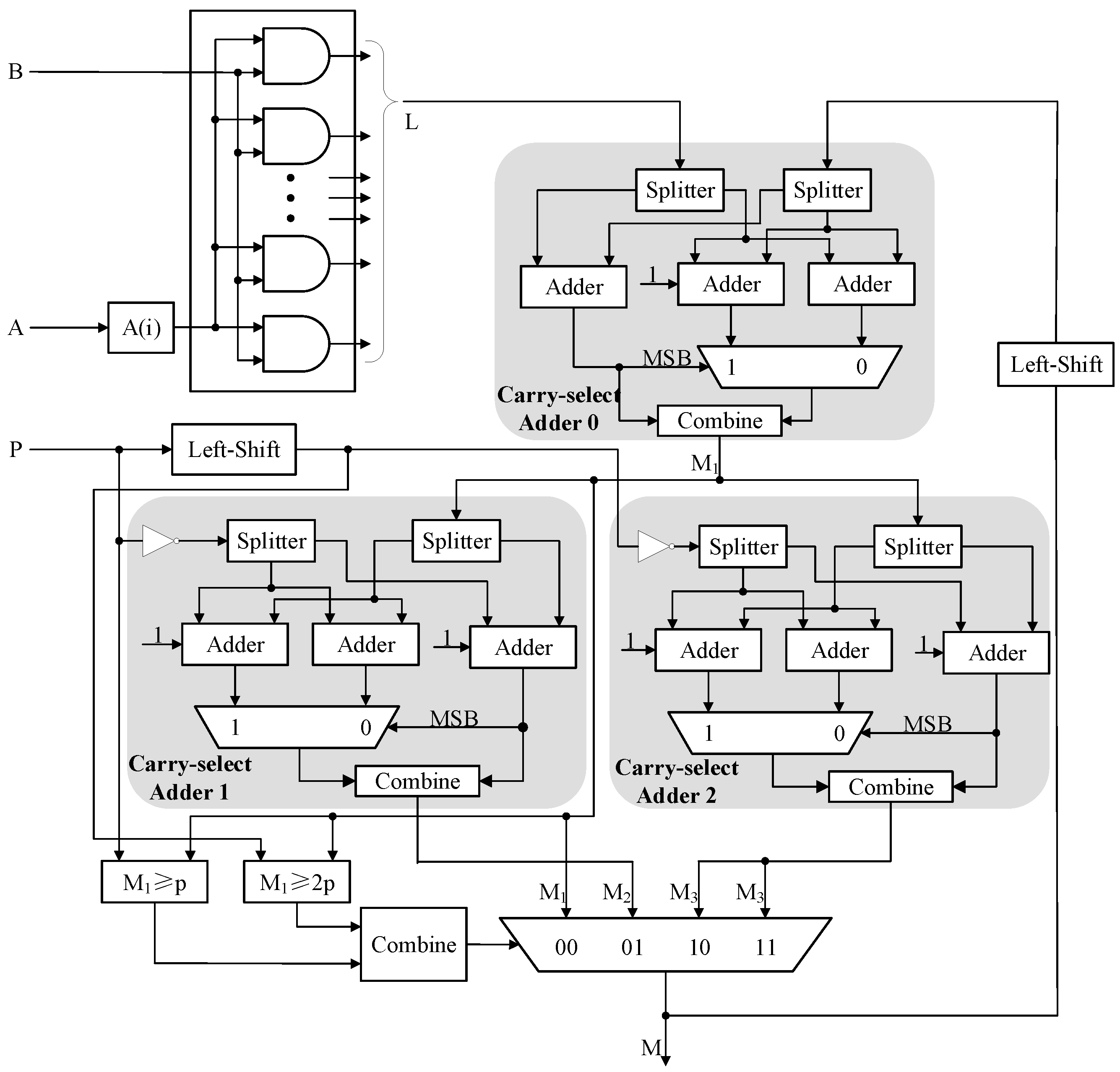
Figure 1 shows the architecture of our proposed modular multiplier.
Here, 2 × p and 2 × M are calculated by the left-shift operation. A [ i ] × B is calculated by AND operation bit-by-bit. Additionally, three carry-select adders are adopted in the architecture to perform addition and subtraction operands, where carry-select adder 0 performs M 1 = M 0 + L , carry-select adder 1 performs M 2 = M 1 p , and carry-select adder 2 performs M 3 = M 1 p . The multiplexer selects the intermediate result by the output of the comparator in each iteration round.
The carry-select adder avoids the series connection of internal adders by the pre-calculation methods, efficiently reducing the circuit latency. Take the M 1 = M 0 + L operation as an example, the calculation process of carry-select Adder 0 in the modular multiplier is based on the following equations. Let M 0 = ( m n 1 , m n 2 , , m 1 , m 0 ) 2 and L = ( l n 1 , l n 2 , , l 1 , l 0 ) 2 , the splitters divide each of them into two parts as
M 0 { M h ( m n 1 , m n 2 , , m n 2 ) , M l ( m n 2 1 , , m 1 , m 0 ) } , L { L h ( l n 1 , l n 2 , , l n 2 ) , L l ( l n 2 1 , , l 1 , l 0 ) } .
Then two adders perform the calculation M h + L h , assuming the carry-in is 0 and 1, respectively. Meanwhile, the third adder performs M l + L l in parallel, which dominates the correct carry-in.
S l = M l + L l , S h 0 = M h + L h , S h 1 = M h + L h + 1 .
The multiplexer selects the correct S h between S h 0 and S h 1 , once the correct carry-in is known.
S h = S h 0 , M S B ( S l ) = 0 ; S h 1 , M S B ( S l ) = 1 .
Finally, the result M 1 is obtained by combining S h and S l as
M 1 { S h ( m n 2 , , m 1 , m 0 ) , S l ( m n 2 1 , , m 1 , m 0 ) } .
In order to perform the subtraction, carry-select adder 1 and carry-select adder 2 require operands p and p to be 2’s complement representation. Thus p and p are inverted bit-by-bit, and an extra 1 is added to both carry-select adders.
In addition to modular multiplication, the modular square is also a complicated operation in ECSM. The circuit area of architecture designed explicitly for modular square is essentially the same as that of modular multiplication. However, according to Algorithm 2, except for the DBLU operation that was executed only once at the beginning of ECSM, all other operations require more multiplications than squares, leading to lower utilization of the specific modular square unit. Consequently, we use a modular multiplier to perform the modular square by entering identical operands to A and B shown in Figure 1.

3.1.2. Modular Divider

In order to avoid the frequent modular division in the ECSM, Jacobian coordinates are used to represent the participating points and the intermediate processing results. However, the final result must be converted to the affine coordinate representation before the ECSM is finished, which requires a modular division according to Equation (5).
To reduce computational complexity and area occupation, we use the binary inversion algorithm (BIA) [26], which is accomplished by addition, subtraction, and shifting operations. The computation of BIA is based on the following equation.
g c d ( A , p ) = 1 e x i s t x , y A × x + p × y = 1 ,
where x is the inverse of A. In order to derive the Equation (17), the BIA constructs an iteration with A and p. During the iterations, it can be obtained by performing divisions and subtractions on the following equations
A × x 1 + p × y 1 = u , A × x 2 + p × y 2 = v .
Let A B 1 and p be the inputs to the BIA, the Equation (17) will become
g c d ( A B 1 , p ) = 1 e x i s t x , y A B 1 × x + p × y = 1 .
So the inverse x is ( A B 1 ) 1 = B A 1 . Additionally, in the first iteration of the BIA, x 1 = 1 , x 2 = 0 , the Equation (18) can be written as
A B 1 × 1 + p × 0 = A B 1 , A B 1 × 0 + p × 1 = p .
By multiplying B to both sides of the equation, the Equation (20) becomes
A B 1 × B + p × 0 = A , A B 1 × 0 + p × 1 = p .
where u = A , v = p , x 1 = B , and x 2 = 1 .
So we modify the initialization of the BIA with x 1 = 1 x 1 = B , and implement the modular division operation B A 1 , as shown in Algorithm 4.
Algorithm 4: Binary division algorithm over F p
Electronics 11 02234 i004
The variables u, v, x 1 , and x 2 are updated in each iteration until the final output condition is satisfied. The u and v will remain in the range of 0 and p, but x 1 and x 2 may be out of this range, so additional m o d p operations are required. The equations to obtain u, v can be summarized as
u = u , u / 2 , ( u v ) / 2 , v = v , v / 2 , ( v u ) / 2 .
In the implementation of Equation (22), divisions are performed by right-shift units. A comparator is used to accomplish the comparison of u and v, and the output is used as one of the conditions for multiplexers. The parity determination for intermediate variables is performed by checking the least significant bit (LSB) value. LSB = 0 represents the variable is even, while LSB = 1 represents the variable is odd. The combine unit concatenates all the conditions for the multiplexer into a 2-bit input.
On the other hand, x 1 , x 2 can be evaluated as
x 1 = x 1 / 2 , ( x 1 + p ) / 2 , ( x 1 x 2 ) / 2 m o d p , ( x 1 x 2 + p ) / 2 m o d p , x 2 = x 2 / 2 , ( x 2 + p ) / 2 , ( x 2 x 1 ) / 2 m o d p , ( x 2 x 1 + p ) / 2 m o d p .
To perform the m o d p operation in Equation (23), the pre-calculation method is used to reduce the carry chain length, which insert ( x 2 x 1 + 2 p ) / 2 and ( x 2 x 1 + 2 p ) / 2 calculations to the architecture. The architecture of the proposed modular divider is shown in Figure 2.

3.2. Improvement in Co-Z Arithmetic

The computation parallelism and critical calculation path analysis are the basis for determining the hardware scheduling scheme of the ECSM in this paper. We expand ZADDC, ZADDU, and DBLU operations into a step-by-step form base on a single modular multiplier and use directed acyclic graphs (DAG) to represent the operational process of these algorithms.
The DAG of the ZADDC operation is shown in Figure 3. The vertex number in the DAG corresponds to the step number in the corresponding algorithm. The SQ and M in solid vertices represent square and multiplication, while the A and S in dotted vertices represent addition and subtraction. Multiplication takes many more clock cycles than addition and subtraction in the prime finite field. Thus we select the number of multiplications as the critical calculation path length. Furthermore, the DAGs that omit A and S operations are also presented to facilitate observation.
As can be seen in Figure 3, the critical calculation path contains 1 SQ, 2 M, and 5 A/S (1→2→3→7→8→21→22→23). While A and S are omitted, as shown in Figure 3b, the critical path length is 3.
When ZADDC is executed for the first time in Algorithm 2, its input comes from the output of DBLU. Moreover, during the whole iteration, the output of ZADDC and ZADDU are used as each other’s input. Therefore, we improve the ZADDC operation by dividing part of incipient calculations to the end of DBLU and ZADDU. Part of the incipient calculations is inserted into the end of ZADDC. In the case of multiple multipliers, this modification improves the parallelism of ZADDC operation without affecting the critical path length of DBLU and ZADDU operations.
The DAG of improved ZADDC is shown in Figure 4. S-INS and SQ-INS calculations are from the ZADDU operation. The improved ZADDC operation contains 13 multiplication paths with the same length and the critical path length is 2.
Meanwhile, ZADDU and DBLU operations are also redistributed. The DAGs are shown in Figure 5. The improved ZADDU operation contains eight multiplication paths with the same length and the critical path length is two. DBLU operation is executed only once at the beginning of Algorithm 2. So the calculation time of DBLU is negligible compared to the whole algorithm execution time. The improved DBLU operation contains nine multiplication paths, and the critical path length is three.

3.3. Hardware Development of ECSM

Our proposed lightweight ECSM architecture consists of a finite field arithmetic unit and an ECSM scheduling unit based on Algorithm 2. This section presents a compact ECSM scheduling based on four modular multipliers, which reduces the overall clock cycles required for the ECSM.

3.3.1. Finite Field Arithmetic Unit

The finite field arithmetic unit (FFAU) performs all the essential finite field operations, consisting of the modular adder/subtracter, modular multiplier, and modular divider. The architecture of modular adder/subtracter in the FFAU uses the conventional design in [8]. With this architecture, modular adder and subtracter are combined in the same module, and an external “a/s” input port is added to control which operation is performed by the module. The entire modular adder/subtracter is composed of combinational logic, thus the result can be cached directly at the adjacent clock after the operands are prepared. In contrast, both the modular multiplier and divider require an iterative calculation to complete the corresponding operation.
In the FFAU, multiple modular additions and subtractions can be performed during the process of modular multiplication and division. Besides, the modular division is performed only once in an ECSM according to Algorithm 2. So one modular adder/subtractor and one modular divider are sufficient for our design.
The critical path length can be reduced by analyzing the critical calculation path and rationally reformulating the algorithm. However, the corresponding number of modular multipliers may increase as well. The most frequently executed operations in Algorithm 2 are the ZADDC and ZADDU operations in the iteration. Table 2 shows the calculation rounds and utilization efficiency with different numbers of modular multipliers based on the improved ZADDC and ZADDU operations in the Section 3.2.
From Table 2, it can be seen that four modular multipliers can complete a single iteration in an ECSM with the minimum calculation rounds. Moreover, when more than four multipliers are adopted, the utilization efficiency drops significantly with no increase in calculation speed. Therefore, to take full advantage of the improved ZADDC and ZADDU, four independent multipliers are integrated into the FFAU. This parallel design benefits from the low resource consumption of our proposed modular multiplier.
Consequently, the composition of FFAU and the functions of each component are shown in Table 3. The FFAU can simultaneously perform up to four modular multiplications, one modular division, and one modular addition/subtraction.

3.3.2. ECSM Scheduling Unit

The ECSM scheduling unit (ECSM-SCU) controls the modular components in the FFAU to perform basic finite field operations with an efficient state machine and caches intermediate results with a register group. Our proposed ECSM-SCU is based on the Algorithm 2 and improved co-Z arithmetic in Section 3.2.
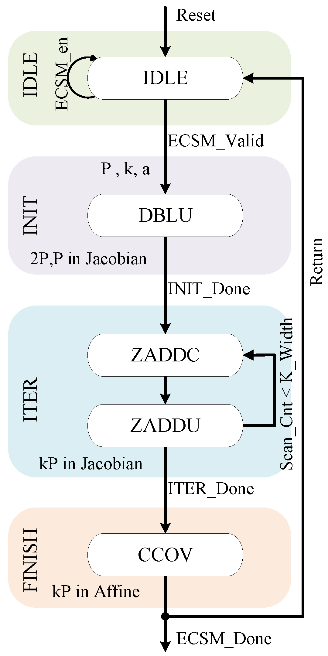
Figure 6 shows the transitions of the state machine used to execute the ECSM. It consists of idle state (IDLE), initialization state (INIT), iteration state (ITER), and finish state (FINISH). In IDLE, the ECSM-SCU is on standby, waiting for an ECSM request. It moves to the INIT after receiving an ECSM request, as well as the secret key and coordinates of point P are cached. A DBLU operation generates P and 2 P in the Jacobian coordinate with the same Z coordinate. Then the ECSM-SCU executes a transition to ITER for the iteration of ZADDC and ZADDU operations. P and 2 P in INIT are used as the input to the ZADDC operation in the first iteration. Then the input–output connection between ZADDC and ZADDU operations in the following iterations will depend on the bit-by-bit scan of the secret key. In addition, ZADDU operations generate the results that satisfy the Montgomery ladder during the iteration. Finally, the state transitions to FINISH, and ECSM-SCU finishes the entire ECSM after converting the final results from Jacobian to affine coordinates. After completing the final output, the state returns to the IDLE, waiting for the next ECSM request.
The most prominent part of the ECSM-SCU is the scheduling of co-Z arithmetic which directly dominates the speed of the ECSM. Although the architecture and number of modular components have been determined, efficient coordination between the modular multiplier and modular adder/subtracter in hardware scheduling can still reduce the clock cycles. Our design principle is to reduce clock cycles, register usage, and keep the modular operations in the FFAU as parallel as possible. Figure 7 shows the details of the co-Z arithmetic scheduling in ECSM-SCU.
MULTIPLICATION STAGE (MS) in Figure 7 represents a stage where modular multipliers in FFAU complete 2~4 modular multiplications in parallel. In an MS, there is no correlation between the four modular multiplications, and each modular multiplier can perform at most one modular multiplication. Every MS starts with a modular multiplication and ends while operands of the first modular multiplication in the following MS are obtained. So the adjacent MS are interrelated and also gradually progressive. In addition, the coordinate conversion from Jacobian to affine coordinates needs to be completed after the last iteration. In order to further improve computational parallelism, two modular multiplications and one modular subtraction in the coordinate conversion are inserted into the MS of ZADDU without affecting the performance of ZADDU operations, as shown in Figure 7c.
In the ECSM-SCU, nine n-bit registers are used to cache the intermediate results. As shown in Table 3, a modular multiplication takes n clock cycles. Therefore the ECSM-SCU will select an unoccupied register to cache the operation result at the n + 1 th clock cycle after starting a modular multiplication. Additionally, for a modular addition/subtraction, the fastest operation for the modular adder/subtracter [8] in the FFAU is to cache the result at the adjacent clock cycle after the operands are prepared. However, the modular adder/subtracter contains a longer carry chain than our proposed modular multiplier, which has an adverse effect on the timing.
In order to reduce the critical path length without consuming more area, we optimize it by scheduling and timing constraints. Firstly, R 8 and R 9 are designated as the modular addition and subtraction buffer, respectively, thus the multiplexer generated while transferring to different registers is eliminated, and the fan-out and path delay are reduced. Then, MulticyclePaths constraints are set from all registers to R 8 / R 9 , improving the delay requirements of the modular adder/subtracter. Meanwhile, a modular addition/subtraction is executed with two clock cycles by ECSM-SCU. This optimization has a very small impact on the overall ECSM computing time since the modular addition/subtraction is scheduled to be executed during the modular multiplication which requires n + 1 clock cycles in ECSM-SCU.
As a result, the DBLU operation is performed once with 3 MS and 3 n + 18 clock cycles in INIT. Additionally, in ITER, the serial ZADDC and ZADDU operations are iterated n 1 rounds, each iteration takes 4 MS and 4 n + 26 clock cycles. Finally, COOV takes 5 modular multiplications and 1 modular division with 6 n + 7 clock cycles. Therefore, the MS and total clock cycles (CC) consumed for a single ECSM can be calculated as
M S E C S M = M S D B L U + ( n 1 ) × ( M S Z A D D C + M S Z A D D U ) + M S C C O V = 3 + ( n 1 ) × ( 2 + 2 ) + 6 = 4 n + 5 C C E C S M = C C D B L U + ( n 1 ) × ( C C Z A D D C + C C Z A D D U ) + C C C C O V = ( 3 n + 18 ) + ( n 1 ) × [ ( 2 n + 15 ) + ( 2 n + 11 ) ] + ( 6 n + 7 ) = 4 n 2 + 31 n 1

4. Resistance against Side-Channel Attacks

Side-channel attacks are based on observing the side-channel information leakage (computation latency, power consumption, electromagnetic emissions, etc.) to decipher the entire or partial secret key, it depends on the operation being executed or the data being handled [40]. This section analyzes the resistance of our proposed ECSM architecture against several simple side-channel attacks. It should be noted that there are many branches of side-channel attacks, we only analyze several simple attacks that our proposed ECSM architecture can resist. We recommend referring to [37] for more information, which summarizes the state-of-the-art ECSM methods on the prime field (including Algorithm 2, which we adopted) against various side-channel attacks.

4.1. Passive Attacks

In the typical timing attack applied to ECC cryptosystems, the attacker relies on the weakness that different key bit values during the iterations result in different computation latency [44]. On the other hand, the SPA attack applied to the ECC cryptosystem is based on the power consumption at a certain time related to the point operation being performed, which leaks the key bit value being manipulated [40]. Thus the attacker can decipher the secret key by monitoring and analyzing the real-time power consumption of the device. Similar to the timing attack, the SPA attack requires the cryptosystems to use an unbalanced ECSM method [45].
However, our proposed ECSM architecture is based on the balanced Montgomery ladder algorithm, and it does not execute any conditional branch statement. Both ZADDC and ZADDU operations are performed with the same sequence in every iteration. As shown in Table 3, the clock cycles required for ZADDC and ZADDU execution are only related to the bit width of the prime field. Therefore, our proposed ECSM architecture is resistant to timing and SPA attacks.

4.2. Active Attacks

The safe-error attack is an active attack that relies on introducing particular errors to the cryptosystem and then observing whether the result is safe or error. The C-type safe-error attack applied to ECSM cryptosystem requires the attacker to introduce computational error to interfere with the execution of the ECSM method [35], which poses a threat to the ECSM methods that utilize dummy operations to resist SPA attacks. The M-type safe-error attack requires the attacker to introduce memory error into the device, the caching of any unnecessary key-related computation may expose the cryptosystem to this attack [46].
Since Algorithm 2 in our proposed design has no dummy operations and adopts the modified method proposed in [47] to resist M-type safe-error attack, any error introduced to either the ECSM-SCU or the registers will result in the error output. So our proposed ECSM architecture is resistant to safe-error attacks.

5. Overall Architecture and Implementation Results

This section presents the implementation results of our proposed lightweight ECSM architecture. The architecture consists of an ECSM-SCU and an FFAU, as shown in Figure 8. The ECSM-SCU is responsible for controlling the entire ECSM process, and the FFAU is used to perform the bottom layer finite field operations over F p . It supports the ECSM for random Weierstrass curves over F p .
The implementation of our proposed design has been done in Verilog HDL and verified using the Synopsys VCS simulator. Synthesizing, mapping, placing, and routing are done using Xilinx Vivado 2022. Table 4 shows the overall performance of the implementation achieved for a field size up to 256-bit on the Kintex-7 FPGA platform. It includes the latency for each ECSM ladder step over four standard ECC prime sizes: 160-bit, 192-bit, 224-bit, and 256-bit. In addition, our design is entirely based on the LUTs without using any integrated resources in FPGA such as DSP or BRAM. Thus it can be migrated to other FPGA platforms or even standard cells on ASIC technologies.
Moreover, for a comprehensive comparison with other similar works, our proposed design is implemented on several standard Xilinx 7-series FPGA platforms such as Virtex-7 (XC7VX690T), Kintex-7 (XC7K325T), and Zynq (XC7Z045), which supports ECSM operations for a field size up to 256-bit. The hardware resource consumption of the implementation results is shown in Table 5. The implementation consumes similar resources in the three FPGA platforms. Therefore, in practical applications, our lightweight architecture can be easily integrated into other hardware designs that require ECC cryptosystem service.
Table 6 shows the implementation results and performance comparison analyses with similar designs. Our proposed design has similar implementation results on three 7-series platforms. A single ECSM operation is performed with 1.73 ms at 156.3 MHz, 1.70 ms at 158.7 MHz, and 1.80 ms at 149.7 MHz on Kintex-7, Virtex-7, and Zynq FPGA, respectively, and the resource consumption is around 6.5k slices in Kintex-7 FPGA, 6.4k slices in both Virtex-7 and Zynq FPGA. It is worth mentioning that the implementation result on Virtex-7 has the best performance with the area-time product (ATP) as low as 10.88. In Table 6, designs in [6,8,11,12,19,20] are entirely LUTs-based. Additionally, designs in [7,9,14,15] use the integrated IPs in Xilinx FPGA to improve processor performance.
In the ECC cryptosystem design for IoT applications, Kudithi et al. [8] proposed an area-efficient, high-speed implementation of ECC processor in affine coordinates over NIST prime fields F 224 and F 256 . It takes 2.70 ms and 3.73 ms for a single ECSM operation in F 224 and F 256 on Xilinx Kintex-7 FPGA, respectively. In 2020, Kudithi further improved the performance of prior design in [6] by utilizing mixed-Jacobian coordinates, increasing the number of multipliers to four, and optimizing the scheduling of ECSM operation. The new design reduces the time to 2.44 ms with a 1k external slices consumption in F 256 . However, the designs in [6,8] are based on the left-to-right binary method which is susceptible to SPA, and these designs only support NIST prime filed F 224 and F 256 . Our design reduces the time by 30% and increases the throughput rate by 41% with similar slices consumption. Furthermore, our design is resistant to side-channel attacks and supports random curves over a general prime field. Thus our proposed ECSM architecture is more suitable for the requirements of IoT applications.
The design in [11] consumes 11.3k slices on Kintex-7 FPGA, and takes 3.27 ms at a frequency of 121.5 MHz to perform a single ECSM operation. Marzouqi et al. [12] took advantage of the redundant-signed-digit (RSD) representation of operands to reduce the latency of the adders used in architecture. It consumes 34.6k LUTs, runs at a frequency of 160 MHz, and takes 2.26 ms to perform a single ECSM operation. Our design is superior in both area and time compared to this design. Hu et al. [19] designed a lightweight ECC processor with 9.4k slices in Virtex-4 FPGA, which may achieve less resource consumption in a new FPGA platform. However, it takes a long time to perform ECSM operation due to its low frequency of 20.4 MHz and 610k clock cycle consumption. Compared with all these lightweight LUT-based ECC processors, our design achieves the fewest clock cycles and time through compact scheduling and has the highest throughput rate.
In terms of the area occupation, the processors in [7,9] consume relatively fewer resources in all the designs that use integrated IPs in Xilinx FPGA. Wu et al. [7] designed a fast and unified ECC processor for five NIST primes. The authors proposed a word-based modular divider and used a scalable multiplication algorithm to support integers of different lengths. This design employs 8.4k slices and 32 DSPs and achieves a time of 0.53 ms in Virtex-7 FPGA. Loi et al. [9] presented an ECC processor that supports 5 prime fields and 10 binary fields NIST curve. All the modular components in their design can be configured in two modes to support prime or binary fields operation. The design can perform an ECSM in 1.38 ms and occupy 2.3k slices, 25 DSPs, and 5 BRAM in Virtex-5 FPGA. Awaludin et al. [14] proposed the fastest high-performance ECC processor over F 256 . It only takes 0.14 ms to perform a single ECSM with 7.1k slices, 136 DSPs, and 15 BRAM. Asif et al. [15] proposed an RSD-based ECC processor resort to a serial-parallel modular reduction architecture for the performance balance of time and area. Their design achieves 0.73 ms at a frequency of 86.6 MHz with the utilization of 18.8k LUTs and as many as 500 DSPs in Virtex-7 FPGA. It must be noted that there is no standard method to evaluate the equivalent resource occupation relationship between the DSPs and slices. We adopt the method with the lowest number of equivalent slices in [6] to evaluate the area occupation. Additionally, our implementation in Virtex-7 FPGA has the smallest ATP compared to the other designs in Table 6. Shah et al. [20] also proposed an RSD-based ECC processor. A combination of the co-Z arithmetic and Montgomery ladder algorithm with four radix-4 RSD-based Montgomery multipliers is applied to perform ECSM operations. In Shah’s design, the RSD-based adder/subtractor, Montgomery multiplier, and divider make it possible to complete a single ECSM operation in just 0.84 ms without consuming any DSPs. However, these RSD-based components, especially the Montgomery multiplier which requires additional logic to convert operands to Montgomery form, lead to a high resources occupation with 13.3k slices. In contrast to this design, our proposed lightweight ECC processor achieved a 48% reduction in an area with similar ATP.

6. Conclusions

In this paper, we have proposed a novel lightweight ECSM architecture for random Weierstrass curves over prime field F p . To achieve low resource consumption, we utilized the adder-based modular multiplier, divider, and adder/subtracter to perform finite field operations. Furthermore, the architectures of modular multiplier and divider are optimized by pre-calculation technology, which decreases the critical path latency and improves the performance of ECSM architecture. Additionally, we also presented compact scheduling of the Montgomery ladder with co-Z arithmetic based on four modular multipliers, which only requires about 4 n 2 + 31 n 1 clock cycles ( 4 n + 5 rounds modular multiplication) for a single ECSM. Our proposed design is implemented in Xilinx Kintex-7, Virtex-7, and Zynq FPGA platforms, utilizing 6.4~6.5k slices without DSPs or BRAMs and takes 1.73 ms, 1.70 ms, and 1.80 ms for an ECSM over F 256 , respectively. The design is based on the direction of low resource consumption, high security, and high portability, making it suitable for IoT applications or other lightweight embedded devices.

Author Contributions

Methodology and writing—original draft preparation, Y.H.; software and writing—review and editing, Y.H. and R.J.; data curation and validation, Y.H., M.M. and S.H.; visualization and project administration, S.H. and J.Z.; supervision and investigation, S.Z. and W.W. All authors have read and agreed to the published version of the manuscript.

Funding

This work was supported in part by the Chongqing Natural Science Foundation under Grant cstc2021jcyj-msxmX1090.

Institutional Review Board Statement

Not applicable.

Informed Consent Statement

Not applicable.

Conflicts of Interest

The authors declare no conflict of interest.

Appendix A. Co-Z Algorithm

The ZADDC, ZADDU, and DBLU operations without Z coordinates are shown in Algorithm A1, Algorithm A2 and Algorithm A3, respectively.
Algorithm A1: ZADDC without Z coordinate
Input: P ( X p , Y p ) and Q ( X q , Y q )
Output: S P + Q , S ¯ P Q ;
1 A = ( X p X q ) 2 ;
2 B = ( Y p Y q ) 2 , C 1 = X p A , C 2 = X q A ;
3 X p + q = B C 1 C 2 , D = Y p ( C 1 C 2 ) ;
4 Y p + q = ( Y p Y q ) ( C 1 X p + q ) D , B ¯ = ( Y p + Y q ) 2 ;
5 X p q = B ¯ C 1 C 2 ;
6 Y p q = ( Y p + Y q ) ( C 1 X p q ) D ;
7 S ( X p + q , Y p + q ) , S ¯ ( X p q , Y p q ) ;
8return S , S ¯
Algorithm A2: ZADDU without Z coordinate
Input: P ( X p , Y p ) and Q ( X q , Y q )
Output: S P + Q , P ˜ P ;
1 A = ( X p X q ) 2 ;
2 B = ( Y p Y q ) 2 , C 1 = X p A , C 2 = X q A ;
3 X p + q = B C 1 C 2 , D = Y p ( C 1 C 2 ) ;
4 Y p + q = ( Y p Y q ) ( C 1 X p + q ) D ;
5 S ( X p + q , Y p + q ) , P ˜ ( C 1 , D ) ;
6return S , P ˜
Algorithm A3: DBLU without Z coordinate
Input: P ( X p , Y p )
Output: 2 P , P ˜ P , ;
1 A = X p 2 , B = Y p 2 ;
2 C = B 2 , M = 3 A + a ;
3 D = X p C , E = 8 C ;
4 N = 4 D ;
5 X 2 p = M 2 2 N ;
6 Y 2 p = M ( N X 2 p ) E ;
7 2 P ( X 2 p , Y 2 p ) , P ˜ ( N , E ) ;
8return 2 P , P ˜

References

  1. Rivest, R.; Shamir, A.; Adleman, L. A method for obtaining digital Signatures and public key Cryptosystems. Commun. ACM 1978, 21, 120–126. [Google Scholar] [CrossRef]
  2. Koblitz, N. Elliptic curve cryptosystems. Math. Comput. 1987, 48, 203–209. [Google Scholar] [CrossRef]
  3. Miller, V.S. Use of elliptic curves in cryptography. In Conference on the Theory And Application of Cryptographic Techniques; Springer: Berlin/Heidelberg, Germany, 1985; pp. 417–426. [Google Scholar]
  4. Barker, E.; Dang, Q. Nist Special Publication 800-57 Part 1, Revision 5: Recommendation for Key Management: Part 1–General; NIST: Gaithersburg, MD, USA, 2020; p. 58.
  5. Rodríguez-Henríquez, F.; Saqib, N.A.; Pérez, A.D.; Koc, C.K. Cryptographic Algorithms on Reconfigurable Hardware; Springer Science & Business Media: Berlin/Heidelberg, Germany, 2007. [Google Scholar]
  6. Kudithi, T. An efficient hardware implementation of the elliptic curve cryptographic processor over prime field. Int. J. Circuit Theory Appl. 2020, 48, 1256–1273. [Google Scholar] [CrossRef]
  7. Wu, T.; Wang, R. Fast unified elliptic curve point multiplication for NIST prime curves on FPGAs. J. Cryptogr. Eng. 2019, 9, 401–410. [Google Scholar] [CrossRef]
  8. Kudithi, T.; Sakthivel, R. High-performance ECC processor architecture design for IoT security applications. J. Supercomput. 2019, 75, 447–474. [Google Scholar] [CrossRef]
  9. Loi, K.C.; Ko, S.B. Flexible elliptic curve cryptography coprocessor using scalable finite field arithmetic blocks on FPGAs. Microprocess. Microsyst. 2018, 63, 182–189. [Google Scholar] [CrossRef]
  10. Marzouqi, H.; Al-Qutayri, M.; Salah, K.; Saleh, H. A 65nm ASIC based 256 NIST prime field ECC processor. In Proceedings of the 2016 IEEE 59th International Midwest Symposium on Circuits and Systems (MWSCAS), Abu Dhabi, United Arab Emirates, 16–19 October 2016; pp. 1–4. [Google Scholar]
  11. Hossain, M.S.; Kong, Y.; Saeedi, E.; Vayalil, N.C. High-performance elliptic curve cryptography processor over NIST prime fields. IET Comput. Digit. Tech. 2016, 11, 33–42. [Google Scholar] [CrossRef]
  12. Marzouqi, H.; Al-Qutayri, M.; Salah, K.; Schinianakis, D.; Stouraitis, T. A high-speed FPGA implementation of an RSD-based ECC processor. IEEE Trans. Very Large Scale Integr. Syst. 2015, 24, 151–164. [Google Scholar] [CrossRef]
  13. Loi, K.C.C.; Ko, S.B. Scalable elliptic curve cryptosystem FPGA processor for NIST prime curves. IEEE Trans. Very Large Scale Integr. Syst. 2015, 23, 2753–2756. [Google Scholar] [CrossRef]
  14. Awaludin, A.M.; Larasati, H.T.; Kim, H. High-speed and unified ECC processor for generic Weierstrass curves over GF (p) on FPGA. Sensors 2021, 21, 1451. [Google Scholar] [CrossRef]
  15. Asif, S.; Hossain, M.S.; Kong, Y.; Abdul, W. A fully RNS based ECC processor. Integration 2018, 61, 138–149. [Google Scholar] [CrossRef]
  16. Amiet, D.; Curiger, A.; Zbinden, P. Flexible FPGA-based architectures for curve point multiplication over GF (p). In Proceedings of the 2016 Euromicro Conference on Digital System Design (DSD), Limassol, Cyprus, 31 August–2 September 2016; pp. 107–114. [Google Scholar]
  17. Javeed, K.; Wang, X. FPGA based high speed SPA resistant elliptic curve scalar multiplier architecture. Int. J. Reconfigurable Comput. 2016, 2016, 6371403. [Google Scholar] [CrossRef] [Green Version]
  18. Hamburg, M. Faster Montgomery and double-add ladders for short Weierstrass curves. IACR Trans. Cryptogr. Hardw. Embed. Syst. 2020, 189–208. [Google Scholar] [CrossRef]
  19. Hu, X.; Zheng, X.; Zhang, S.; Cai, S.; Xiong, X. A low hardware consumption elliptic curve cryptographic architecture over GF (p) in embedded application. Electronics 2018, 7, 104. [Google Scholar] [CrossRef] [Green Version]
  20. Shah, Y.A.; Javeed, K.; Azmat, S.; Wang, X. A high-speed RSD-based flexible ECC processor for arbitrary curves over general prime field. Int. J. Circuit Theory Appl. 2018, 46, 1858–1878. [Google Scholar] [CrossRef]
  21. Sghaier, A.; Zeghid, M.; Massoud, C.; Ahmed, H.Y.; Chehri, A.; Machhout, M. Fast Constant-Time Modular Inversion over F p Resistant to Simple Power Analysis Attacks for IoT Applications. Sensors 2022, 22, 2535. [Google Scholar] [CrossRef]
  22. Jang, H.S.; Jin, H.; Jung, B.C.; Quek, T.Q. Versatile access control for massive IoT: Throughput, latency, and energy efficiency. IEEE Trans. Mob. Comput. 2019, 19, 1984–1997. [Google Scholar] [CrossRef]
  23. Liu, Z.; Seo, H. IoT-NUMS: Evaluating NUMS elliptic curve cryptography for IoT platforms. IEEE Trans. Inf. Forensics Secur. 2018, 14, 720–729. [Google Scholar] [CrossRef]
  24. Ledwaba, L.P.; Hancke, G.P.; Venter, H.S.; Isaac, S.J. Performance costs of software cryptography in securing new-generation Internet of energy endpoint devices. IEEE Access 2018, 6, 9303–9323. [Google Scholar] [CrossRef]
  25. Di Matteo, S.; Baldanzi, L.; Crocetti, L.; Nannipieri, P.; Fanucci, L.; Saponara, S. Secure elliptic curve crypto-processor for real-time IoT applications. Energies 2021, 14, 4676. [Google Scholar] [CrossRef]
  26. Hankerson, D.; Menezes, A.J.; Vanstone, S. Guide to Elliptic Curve Cryptography; Springer Science & Business Media: Berlin/Heidelberg, Germany, 2006. [Google Scholar]
  27. Dong, X.; Zhang, L.; Gao, X. An efficient FPGA implementation of ECC modular inversion over F256. In Proceedings of the 2nd International Conference on Cryptography, Security and Privacy, Guiyang, China, 16–19 March 2018; pp. 29–33. [Google Scholar]
  28. Al-Haija, Q.; AlShuaibi, A.; Al Badawi, A. Frequency analysis of 32-bit modular divider based on extended GCD algorithm for different FPGA chips. Int. J. Comput. Technol. 2018, 17, 7133–7139. [Google Scholar] [CrossRef] [Green Version]
  29. Yi, S.; Li, W.; Dai, Z. A scalable and efficient hardware architecture for Montgomery modular division in dual field. In Proceedings of the 2016 10th IEEE International Conference on Anti-Counterfeiting, Security, and Identification (ASID), Xiamen, China, 23–25 September 2016; pp. 34–38. [Google Scholar]
  30. Meloni, N. New point addition formulae for ECC applications. In International Workshop on the Arithmetic of Finite Fields; Springer: Berlin/Heidelberg, Germany, 2007; pp. 189–201. [Google Scholar]
  31. Kocher, P.C. Timing attacks on implementations of Diffie-Hellman, RSA, DSS, and other systems. In Annual International Cryptology Conference; Springer: Berlin/Heidelberg, Germany, 1996; pp. 104–113. [Google Scholar]
  32. Kocher, P.; Jaffe, J.; Jun, B. Differential power analysis. In Annual International Cryptology Conference; Springer: Berlin/Heidelberg, Germany, 1999; pp. 388–397. [Google Scholar]
  33. Coron, J.S. Resistance against differential power analysis for elliptic curve cryptosystems. In International Workshop on Cryptographic Hardware and Embedded Systems; Springer: Berlin/Heidelberg, Germany, 1999; pp. 292–302. [Google Scholar]
  34. Hitchcock, Y.; Montague, P. A new elliptic curve scalar multiplication algorithm to resist simple power analysis. In Australasian Conference on Information Security and Privacy; Springer: Berlin/Heidelberg, Germany, 2002; pp. 214–225. [Google Scholar]
  35. Sung-Ming, Y.; Kim, S.; Lim, S.; Moon, S. A countermeasure against one physical cryptanalysis may benefit another attack. In International Conference on Information Security and Cryptology; Springer: Berlin/Heidelberg, Germany, 2001; pp. 414–427. [Google Scholar]
  36. Montgomery, P.L. Speeding the Pollard and elliptic curve methods of factorization. Math. Comput. 1987, 48, 243–264. [Google Scholar] [CrossRef]
  37. Abarzúa, R.; Valencia, C.; López, J. Survey on performance and security problems of countermeasures for passive side-channel attacks on ECC. J. Cryptogr. Eng. 2021, 11, 71–102. [Google Scholar] [CrossRef]
  38. Hutter, M.; Joye, M.; Sierra, Y. Memory-constrained implementations of elliptic curve cryptography in co-Z coordinate representation. In International Conference on Cryptology in Africa; Springer: Berlin/Heidelberg, Germany, 2011; pp. 170–187. [Google Scholar]
  39. Goundar, R.R.; Joye, M.; Miyaji, A. Co-Z addition formulæ and binary ladders on elliptic curves. In International Workshop on Cryptographic Hardware and Embedded Systems; Springer: Berlin/Heidelberg, Germany, 2010; pp. 65–79. [Google Scholar]
  40. Venelli, A.; Dassance, F. Faster side-channel resistant elliptic curve scalar multiplication. Contemp. Math. 2010, 521, 29–40. [Google Scholar]
  41. Montgomery, P.L. Modular multiplication without trial division. Math. Comput. 1985, 44, 519–521. [Google Scholar] [CrossRef]
  42. Knuth, D.E. Art of Computer Programming, Volume 2: Seminumerical Algorithms; Addison-Wesley Professional: Boston, MA, USA, 2014. [Google Scholar]
  43. Amanor, D.N.; Paar, C.; Pelzl, J.; Bunimov, V.; Schimmler, M. Efficient hardware architectures for modular multiplication on FPGAs. In Proceedings of the International Conference on Field Programmable Logic and Applications, Tampere, Finland, 24–26 August 2005; pp. 539–542. [Google Scholar]
  44. Al-Zubaidie, M.; Zhang, Z.; Zhang, J. Efficient and secure ECDSA algorithm and its applications: A survey. arXiv 2019, arXiv:1902.10313. [Google Scholar] [CrossRef]
  45. Ghosh, S.; Mukhopadhyay, D.; Roychowdhury, D. Petrel: Power and Timing Attack Resistant Elliptic Curve Scalar Multiplier Based on Programmable GF(p) Arithmetic Unit. IEEE Trans. Circuits Syst. I Regul. Pap. 2011, 58, 1798–1812. [Google Scholar] [CrossRef]
  46. Yen, S.M.; Joye, M. Checking before output may not be enough against fault-based cryptanalysis. IEEE Trans. Comput. 2000, 49, 967–970. [Google Scholar]
  47. Joye, M.; Yen, S.M. The Montgomery powering ladder. In International Workshop on Cryptographic Hardware and Embedded Systems; Springer: Berlin/Heidelberg, Germany, 2002; pp. 291–302. [Google Scholar]
Figure 1. Architecture of proposed modular multiplier.
Electronics 11 02234 g001
Figure 2. Architecture of proposed modular divider.
Electronics 11 02234 g002
Figure 3. Directed acyclic graph of original ZADDC. (a) Full ops. (b) A and S omitted.
Electronics 11 02234 g003
Figure 4. Directed acyclic graph of improved ZADDC. (a) Full ops. (b) A and S omitted.
Electronics 11 02234 g004
Figure 5. Directed acyclic graph of improved ZADDU and DBLU (A and S omitted). (a) DAG of ZADDU. (b) DAG of DBLU.
Electronics 11 02234 g005
Figure 6. State transition diagram in ECSM-SCU.
Electronics 11 02234 g006
Figure 7. Co-Z arithmetic scheduling in ECSM-SCU. (a) DBLU. (b) ZADDC. (c) ZADDU with coordinate conversion.
Electronics 11 02234 g007
Figure 8. Proposed ECSM architecture.
Electronics 11 02234 g008
Table 1. Co-Z arithmetic function in the Montgomery ladder.
OperationResult 1Result 2Remark
( T 0 , T 1 ) DBLU ( P ) T 0 = 2 P T 1 = P ˜ PD with P update
( T 0 , T 1 ) ZADDU ( P , Q ) T 0 = P + Q T 1 = P ˜ PA with P update
( T 0 , T 1 ) ZADDC ( P , Q ) T 0 = P + Q T 1 = P Q PA with conjugate
Table 2. Modular multiplier number comparison.
NumberCalculation RoundUtilization
ZADDCZADDUZADDCZADDUOverall
1 M86100%100%100%
2 M43100%100%100%
3 M3288.8%100%93.3%
4 M22100%75%87.5%
5 M2280%60%70%
Table 3. Modular components in FFAU.
ComponentNumberOperationClock Cycles
Modular Adder/Subtracter1 S = A ± B m o d p 1 *
Modular Multiplier4 M = A × B m o d p n
Modular Divider1 I = B A 1 m o d p 2 n + 1
Notes: * The modular adder/subtracter composed of combinational logic result in a long critical path, thus the timing and scheduling are optimized (please refer to Section 3.3.2 for details).
Table 4. Performance of proposed ECSM architecture on Kintex-7.
Field SizeINITITERFINISHTotalTotal Latency
DBLUZADDCZADDUCCOVClock Cycles@156.3 MHz
1603.19 µs2.14 µs2.12 µs6.19 µs107,3590.69 ms
1923.80 µs2.52 µs2.53 µs7.42 µs153,4070.98 ms
2244.41 µs2.96 µs2.94 µs8.64 µs207,6471.33 ms
2565.03 µs3.37 µs3.35 µs9.87 µs270,0791.73 ms
Table 5. Resource consumption of proposed ECSM architecture (256-bit field size).
PlatformSlice LUTsFlip FlopsSlice
UsedAvailableUsedAvailableUsedAvailable
Kintex-721,039203,800707440,7600647750,950
Virtex-721,176433,2007060866,4006397108,300
Zynq20,692218,6007083437,200635154,650
Table 6. Performance comparison of several ECSM architectures for Weierstrass curve up to 256-bit field size.
DesignsPlatformArea (Slices)Clock CyclesFrequenctTime/ECSMATPThroughput Rate
ProposedKintex-76.5k270k156.3 MHz1.73 ms11.25147.9 kbps
Virtex-76.4k270k158.7 MHz1.70 ms10.88150.6 kbps
Zynq6.4k270k149.7 MHz1.80 ms11.55142.1 kbps
Kudithi et al. [6]Kintex-77.4k300k122.8 MHz2.44 ms18.16104.9 kbps
Virtex-75.5k300k122.8 MHz2.44 ms13.37104.9 kbps
Kudithi et al. [8]Kintex-76.4k464.1k124.2 MHz3.73 ms23.8768.5 kbps
Virtex-75.4k464.1k124.2 MHz3.73 ms20.4568.5 kbps
Hossain et al. [11]Kintex-711.3k397.3k121.5 MHz3.27 ms36.9578.3 kbps
Hu et al. [19]Virtex-49.4k610k20.4 MHz29.84 ms279.68.6 kbps
Marzouqi et al. [12] 1Virtex-534.6k (LUTs)361.6k160 MHz2.26 ms19.55113.3 kbps
Shah et al. [20]Virtex-513.3k144.5k172 MHz0.84 ms11.17304.8 kbps
Wu T et al. [7] 2Virtex-78.4k + 32 DSPs162.9k310 MHz0.53 ms4.45/14.63 3486.6 kbps
Virtex-67.7k + 32 DSPs162.9k256 MHz0.64 ms4.93/17.22 3402.5 kbps
Loi et al. [9] 2Virtex-52.3k + 25 DSPs + 25 BRAMs214.3k155.3 MHz1.38 ms3.17/24.53 3185.5 kbps
Awaludin et al. [14] 2Kintex-77.1k + 136 DSPs + 15 BRAMs32.3k234.1 MHz0.14 ms0.99/12.78 31829 kbps
Virtex-76.9k + 136 DSPs + 15 BRAMs32.3k232.3 MHz0.14 ms0.97/12.75 31829 kbps
Zynq7.1k + 136 DSPs + 15 BRAMs32.3k156.8 MHz0.21 ms1.49/19.17 31829 kbps
Asif et al. [15] 1,2Virtex-718.8k (LUTs) + 500 DSPs63.2k86.6 MHz0.73 ms3.43/229.37 3350.7 kbps
Notes: 1 4 LUTs are evaluated as 1 slice (34.6k LUTs = 8.64k slices). 2 1 DSP is evaluated as 619 slices [6], and the BRAM resources are ignored. 3 ATP for high performance designs with DSP resources is shown as [Slices × Time]/[(Slices + DSP × 619) × Time].
Publisher’s Note: MDPI stays neutral with regard to jurisdictional claims in published maps and institutional affiliations.

