You are currently viewing a new version of our website. To view the old version click .
Electronics
  • Article
  • Open Access

10 May 2021

Research on an Improved Three-Level SVPWM Modulation Algorithm Based on ID-NPC Topology

and
1
School of Electrical Engineering, Beijing Jiaotong University, Beijing 100044, China
2
School of Electronic and Electrical Engineering, Cangzhou Jiaotong College, Cangzhou 061199, China
*
Author to whom correspondence should be addressed.
This article belongs to the Section Power Electronics

Abstract

The conventional three-level SVPWM (Space Vector Pulse Width Modulation) algorithm is a basic modulation algorithm, which can be performed easily due to clear modulation ideas. Considering different criteria for sectors, however, the basic vector action time is calculated repeatedly, the selection of vector action sequence is cumbersome, and the algorithm execution time is extended as a result of processing by the digital processing chip. In order to better adapt to the PMSM (Permanent Magnet Synchronous Motor) control requirements of the ID-NPC (Improved Diodes Neutral Point Clamped) topology for converter control objects, the sector judgment part, time effect part and vector synthesis part are optimized according to the principles of saving hardware resources and shortening the execution cycle. The vector synthesis optimization algorithm of 2 × amplitude substitution and the vector synthesis algorithm of 1/2 × amplitude substitution are both proposed. Finally, the ID-NPC topology is used to verify the proposed modulation algorithm.

1. Introduction

With the development of high power electronic components, the topology of the PWM (Pulse Width Modulation) converter has changed from two-level, to three-level, to multi-level [1,2]. In the three-level neutral point clamped ID-NPC structure, If the voltage offset is too large, the voltage distribution will be balanced, which will result in increase in the output voltage THD (Total Harmonic Distortion) of the converter and thus damage to switching devices. The voltage fluctuation of the neutral point must not exceed 5% of the DC bus voltage [3]. When the long vector is used, the three-phase connection is connected to the positive bus or negative bus, and there is no connection with the neutral point, no current flows through the neutral point, and the long vector does not affect the neutral point potential [4]. When the medium vector is used, the three phases of the load are connected with the positive and negative buses and the neutral point, and the current flows through the neutral point when the capacitor is charged and discharged, and the influence of the medium vector on the central point potential is uncontrollable under different working conditions of the motor [5]. The influence of small vectors on the neutral point is complex, and the paired redundant small vectors can produce opposite current and opposite influence on the neutral point potential [6,7]. In addition, some non-ideal factors, such as unbalanced capacitance caused by circuit distribution parameters, inconsistent characteristics of switching devices, three-phase asymmetric operation, etc., will also affect the neutral point potential [8]. In order to reduce the NP (Neutral Point) offset, the conventional modulation algorithm must be improved, in accordance with the principles of using long vectors with priority, controlling the applications of short vectors and reducing the applications of medium vectors. The two-level modulation algorithm is simpler than three-level modulation algorithm, and the three-level SVPWM modulation algorithm can be converted into a two-level modulation algorithm [9,10].

2. Improved D-NPC Topology

The improved diode-clamped multilevel topology (ID-NPC) is shown in Figure 1. Each set of main bridge arm consists of six controllable switching elements and two diode clamping elements. The connection between the DC power supply and converter is the same as that of the D-NPC. Taking the U-phase main bridge arm as an example, six switching elements of the main bridge arm are divided into three groups: T11 and T12, T13 and T14, T15 and T16. The drive ports are G11, G13 and G15, respectively. When the drive port G11 is connected, the phase output is Vdc/2 (positive level state); when the drive port G15 is connected, the phase output is 0 (zero level state); when the drive port G13 is connected, the phase output is −Vdc/2 (negative level state). The six controllable switching elements in three groups are connected in turn for three output levels. That is, the elements are connected separately in the positive, negative, and zero level states, without repeated conduction superimposition. The heat on single elements is distributed evenly. Three drive circuits are required for three switching elements in three groups on the main bridge arm, and nine switching drive circuits for a single converter [11].
Figure 1. ID-NPC (Improved Diodes Neutral Point Clamped) topology.
The switching state of the ID-NPC topology is shown in Table 1 below, which is simpler and more intuitive. The switching state table and loss a distribution analysis are based on the U-phase as an example.
Table 1. ID-NPC (Improved Diodes Neutral Point Clamped) level states.

3. Improved Three-Level SVPWM Control Strategy

3.1. Three-Level SVPWM Sequential Synthesis Algorithm

After Clark transformation, the three-phase symmetric voltage is substituted into the formula, U m is the amplitude of the modulation voltage:
[ u α u β ] = U m [ cos ( ω u t ) sin ( ω u t ) ] ,
The sine and cosine values are found in the lookup table of 16-bit. When the reference voltage vector is V15 (HLL, corresponds to (“+” “−” “−”) level state):
u b = 2 3 V dc e j 0 ,
Similarly, in addition to 3 zero vectors, 12 vectors (short vectors) with an amplitude of Vdc/3, 6 vectors (medium vectors) with an amplitude of 3 V dc/3, and 6 vectors (long vectors) with an amplitude of 2Vdc/3 are obtained, as shown in Figure 2 The degree of modulation is defined as M = π | V ref | / 2 V dc . For SVPWM modulation, the ratio of the synthesized voltage vector amplitude V ref to maximum basic vector amplitude 2 V dc / 3 ( V dc / 3 for the 2 × vector modulation algorithm) is 3 / 2 or less within the linear modulation section and [0, 0.907] within the linear modulation section of M . As shown in Figure 2, when θ is within 0–360° and M 0.907 , the SVPWM linear modulation section within the hexagonal incircle [12,13,14].
Figure 2. Synthetic voltage vector range.
As can be seen from the above analysis and Figure 2, the result of SVPWM modulation is a rotating space voltage vector to drive the PMSM to rotate. It is not necessary to determine the specific vector in the sequential synthesis strategy. Instead, only clockwise or counterclockwise modulation at a certain speed is needed. The linear modulation section [0, 0.907] can be divided as follows based on the M: [0, 0.453], (0.453, 0.5], (0.5, 0.907], as detailed below.
M ∈ [0, 0.453] is shown in Figure 3. When M = 0.453 on the dotted line, the resultant voltage vector is in the S1 sector (triangle V15V11V16, consists of six sub regions), S2, S3, S4, S5 and S6 are similar. The vector passes through the area in the counterclockwise direction corresponding to 0–2π: S11→S12→S21→S22→S31→S32→S41→S42→S51→S52→S61→S62. Three basic vectors of adjacent areas are synthesized. The vectors may not start from S11. Synthesis can be performed in the sweep order without sector judgment.
Figure 3. Area related to resultant vector in case of M ∈ [0, 0.453).
M ∈ (0.453, 0.5] is shown in Figure 4. The thin dashed lines indicate the resultant voltage vectors in the S1 sector in the case of M = 0.453 and M = 0.5, respectively. The thick dashed lines indicate one resultant vector in this area. The vector passes through the area in the counterclockwise direction corresponding to 0–2π: S11→S13→S14→S12→S11→S23→S24→S22→S31→S33→S34→S32→S41→S43→S44→S42→S51→S53→S54→S52→S61→S63→S64→S62. Three basic vectors of adjacent areas are synthesized. The vectors may not start from any area. Synthesis can be performed in the sweep order without sector judgment.
Figure 4. Area related to resultant vector in case of M ( 0.453 ,   0.5 ] .
M ∈ (0.5, 0.907] is shown in Figure 5. The thin dashed lines indicate the areas where the vector M = 0.5 passes. The thick dashed lines indicate the area where one resultant vector passes in a counterclockwise order corresponding to 0–2π: S15→ S13→ S14→ S16→ S25→ S23→ S24→ S26→ S35→ S33→ S34→ S36→ S45→ S43→ S44→ S46→ S55→ S53→ S54→ S56→ S65→ S63→ S64→ S66. Similar to the above description, the basic vectors in adjacent areas can be synthesized by the sweep manner without sector judgment.
Figure 5. Area related to resultant vector in case of M ( 0.5 ,   0.907 ] .

3.2. Vector Synthesis Algorithm of 2 × Amplitude Substitution

According to the above analysis, when M ∈ [0, 0.453], the reference vector passes through two areas in one sector; and when M ∈ (0.453, 0.907], the sector where the reference vector passes includes more than two areas. Once the vector passes through one area, a series of switching tubes will change accordingly, resulting in switching losses. In order to further reduce switching losses, the synthesis strategy of 2 × amplitude substitution is proposed by using M ∈ [0, 0.453] in the case of M ∈ (0.453, 0.907].
Take the S1 sector as an example. When a ∈ (0.453, 0.907], a/2 ∈ (0.227, 0.453] is converted to the first case discussed in the previous section. According to the volt-second balance rule (reference vector: Vref, when M = a/2, the corresponding reference vector is Vref/2), get the following formula:
{ V ref / 2 × T s = V 12 × T 12 + V 13 × T 13 + V 11 × T 11 T s = T 12 + T 13 + T 11                                     ,
V α is the x-axis projection of Vref/2 and V β is the y-axis projection of Vref/2. The action time of the adjacent basic vector is calculated as follows:
{ V α × T s = V 12 × T 12 × cos θ + V 13 × T 13 × cos θ + V 11 × T 11 × cos θ V β × T s = V 12 × T 12 × sin θ + V 13 × T 13 × sin θ + V 11 × T 11 × sin θ T s = T 12 + T 13 + T 11 ,
Sort out the coefficients:
{ V α = V 12 × T 12 T s × cos θ + V 13 × T 13 T s × cos θ + V 11 × T 11 T s × cos θ V β = V 12 × T 12 T s × sin θ + V 13 × T 13 T s × sin θ + V 11 × T 11 T s × sin θ T s = T 12 + T 13 + T 11 ,
The reference vector ( V ref ) is equivalent to the synthesis of V 12 × T 12 / T s and V 13 × T 13 / T s . According to the linear invariance, both sides of the Formula (5) are multiplied by 2 at the same time:
{ 2 V α = V 12 × 2 T 12 T s × cos θ + V 13 × 2 T 13 T s × cos θ + V 11 × 2 T 11 T s × cos θ 2 V β = V 12 × 2 T 12 T s × sin θ + V 13 × 2 T 13 T s × sin θ + V 11 × 2 T 11 T s × sin θ 2 T s = 2 T 12 + 2 T 13 + 2 T 11 ,
The two vectors V α and V β can be doubled within the action time of the corresponding basic vector, as shown in Figure 6.
Figure 6. Vector synthesis by vector substitution.
It can be seen from the above figure that the vector Vref/2 is half of Vref, covering 1/4 of the sector. After this vector is doubled, the linear modulation area can be fully covered. The order of the full modulation area is optimized in a counterclockwise order: S11→S12→S21→S22→S31→S32→S41→S42→S51→S52→S61→S62.

3.3. Vector Synthesis Algorithm of 1/2 × Amplitude Substitution

Since short vectors have a complicated impact on the NP unbalance, a vector synthesis algorithm of 1/2 × amplitude substitution is proposed, in which medium and long vectors are synthesized instead of short vectors. The vectors in the areas S11 and S12 can be replaced by 1/2 the amplitude in S13, S14, S15 and S16. In conjunction with the Formulas (3) to (6), the vector Vref is used instead of Vref/2 in Figure 6, i.e., Vref/2 = (1/2)Vref. The derivation process is similar to the vector synthesis algorithm of 1/2 × amplitude substitution.

3.4. Time Effect Optimization

Adjacent basic vectors are synthesized to the equivalent reference voltage vector. The action time of basic vectors is determined according to the principle of volt-second balance. As shown in Figure 4, the area in sector S1 is marked as S11–S16, parts of S11 and S12 are collectively marked as S112, parts of S21 and S22 are collectively marked as S212, parts of S31 and S32 are collectively marked as S312, parts of S41 and S42 are collectively marked as S412, parts of S51 and S52 are collectively marked as S512, parts of S61 and S62 are collectively marked as S612, and other medium and small areas in large areas are marked similarly [15,16]. Each vector in a small area is the synthetic result of three basic vectors, which correspond to the action time T11, T12 and T13, respectively. That is, the basic vectors in 36 small areas in the conventional modulation algorithm correspond to 108 time values, so the time calculation is cumbersome. Each area in S11–S16 is composed of three adjacent vectors. Taking the first area as an example, the corresponding adjacent vectors and action time are shown in Table 2.
Table 2. Adjacent vectors and action Time corresponding to the first area.
The redundant switching sequence of the converter can be changed based on the minimum switching loss or minimum total harmonic distortion (THD) target. In order to achieve low THD, the vector switching sequence of the area S112: V13→V12→V11→V12→V13→V13→V12→V11→V12→V13.
Among six areas (S11–S16), the areas S12–S16 can be obtained by rotating S11 by nπ/3(n = 1, 2, 3, 4, 5). Taking S11 rotation to obtain S12 as an example, the relationship between the space vector and voltage is shown Table 3 below.
Table 3. Relationship between space vector and voltage of the first sector.
The reference vector V ref 1 of the first area is obtained according to the principle of volt-second balance:
{ V ref 1 × T s = V 11 × T 11 + V 12 × T 12 + V 13 × T 13 T s = T 11 + T 12 + T 13 ,
Both sides of the formula are multiplied by the factor e j π / 3 , and the reference vector V ref 1 of the first area is rotated to obtain the reference vector V ref 2 of the second area:
{ V ref 2 × T s = V 21 × T 21 + V 22 × T 22 + V 23 × T 23 T s = T 21 + T 22 + T 23 ,
By comparison, it can be seen that the conduction time is exactly the same for them, and so on. The conduction time is also the same for six areas. Assuming that V ref 1 is composed of u a , u b and u c , then:
{ V ref 1 = 2 3 ( u a + u b × e j 2 π 3 + u c × e j 2 π 3 ) V ref 2 = V ref 1 × e j π 3 = 2 3 ( u b u c × e j 2 π 3 u a × e j 2 π 3 ) ,
The phase voltage relationship of six areas is shown in Table 4.
Table 4. Phase voltage relationship of areas.
Through simplification, all six areas can be mapped to the first area, which can simplify the process and save hardware resources.

4. Simulation and Analysis of Modulation Algorithm Based on ID-NPC

Simulation conditions is shown in Table 5.
Table 5. Simulation conditions.
According to Section 3, the M range is [0, 0.866]. Record the waveform of vector synthesis strategy of 2 × vector substitution in the case of M = 0.8 , and the waveform of vector synthesis strategy of 1/2 × amplitude substitution in the case of M = 0.4 .
PMSM motor parameter setting is shown in Table 6.
Table 6. PMSM motor parameter setting.

4.1. Waveform of Vector Synthesis Algorithm of 2 × Amplitude Substitution

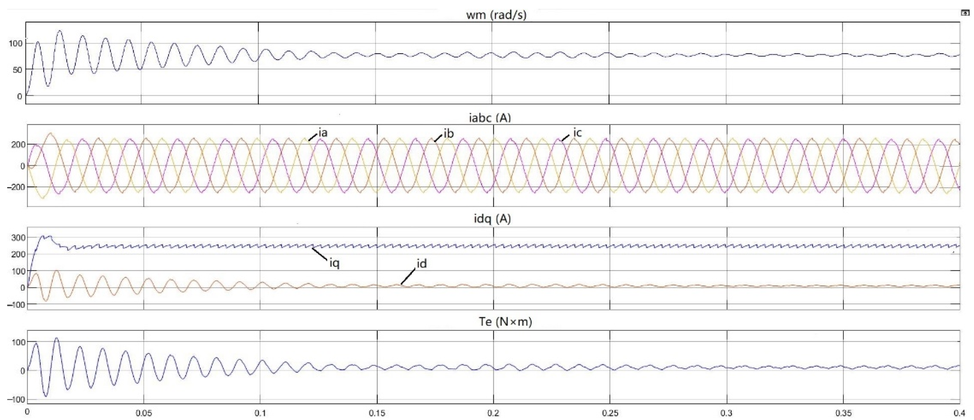
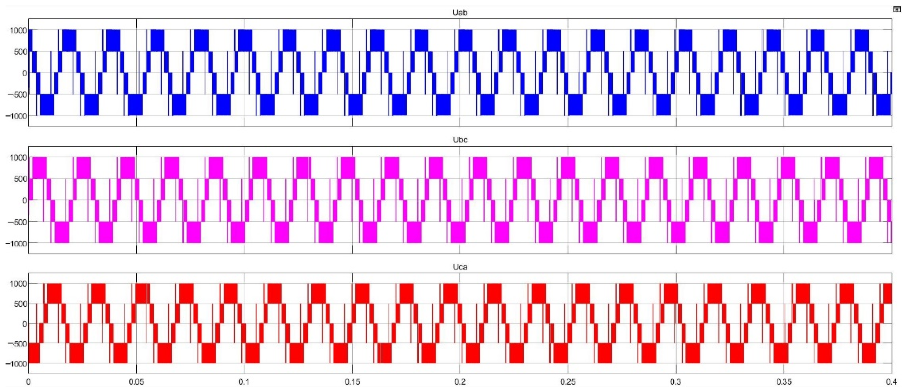
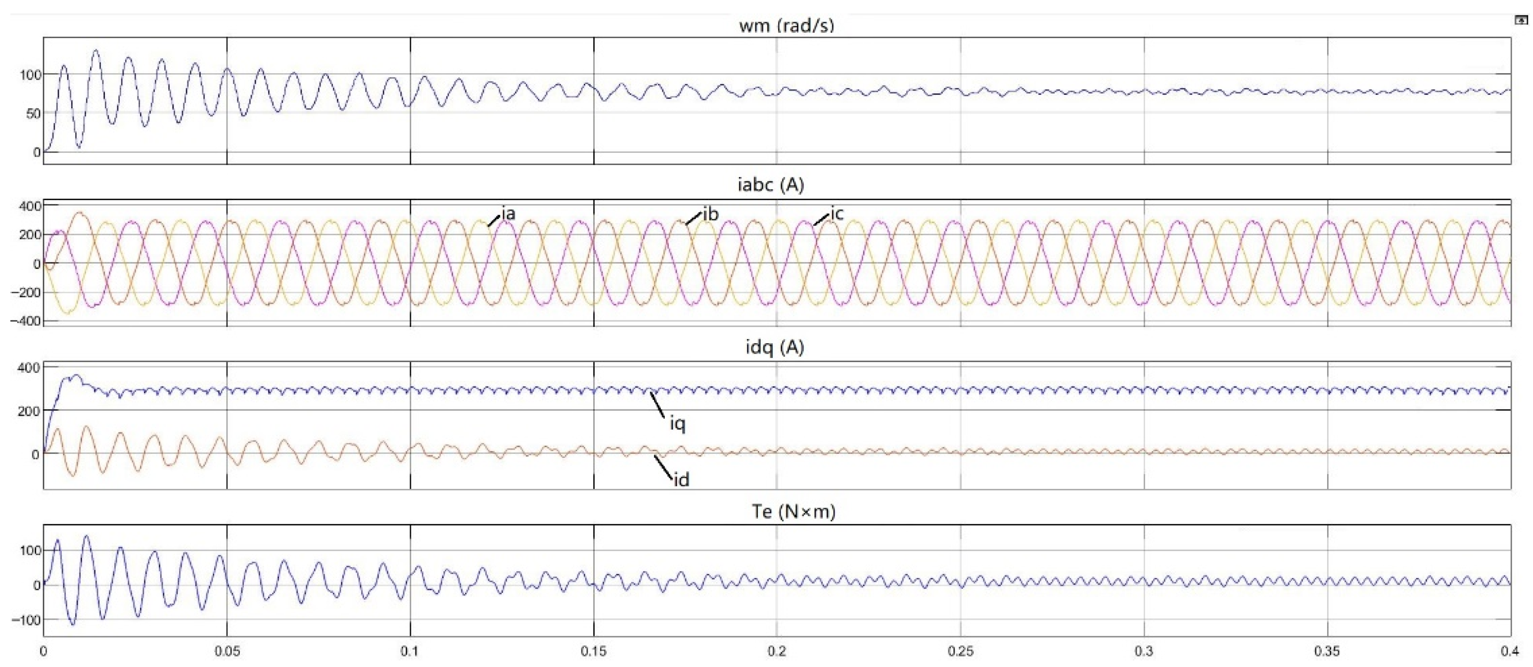
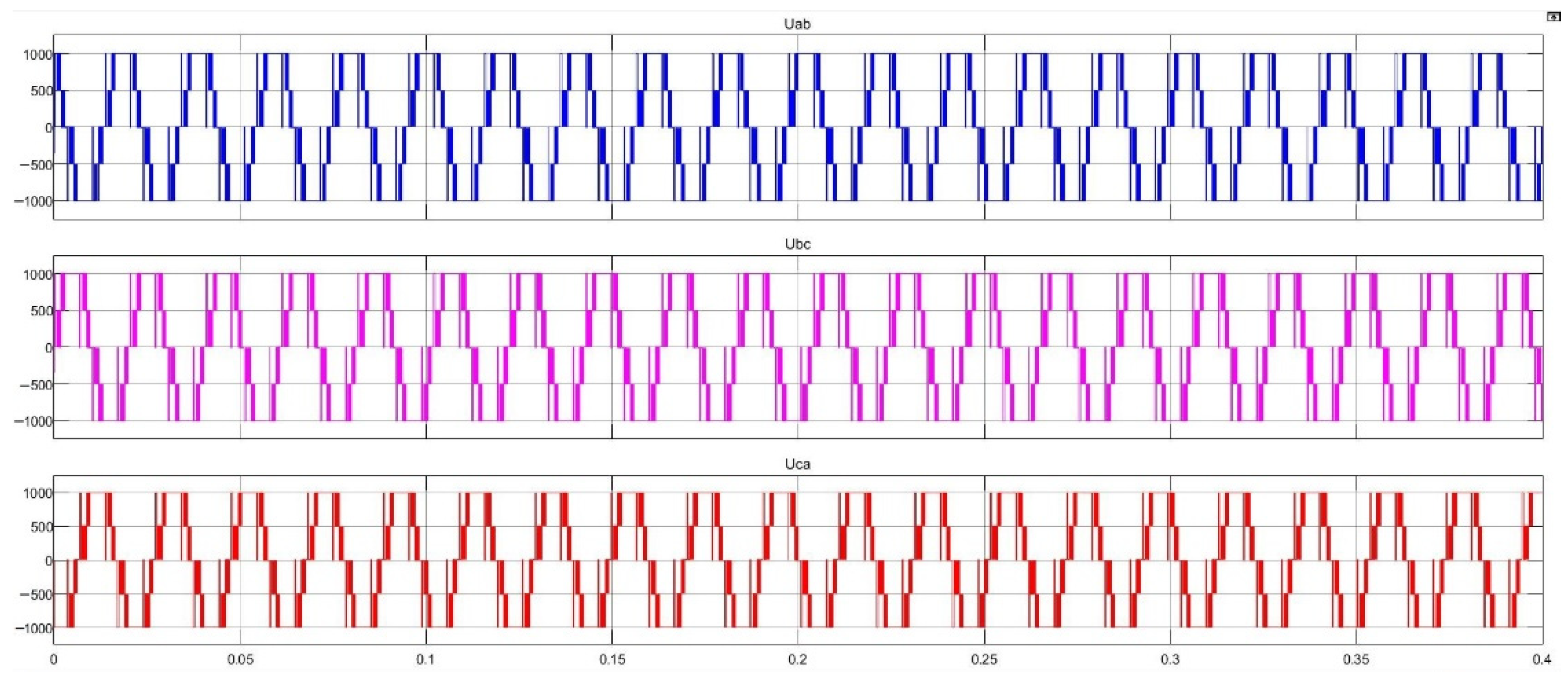
When M = 0.8 in the conventional vector modulation algorithm, the waveforms of the parameters are shown in Figure 7, and the stator voltages u ab , u bc and u ca are shown in Figure 8. In Figure 7, the first part is the speed waveform (Unit: rad/s), the second part is the three-phase current ia, ib, ic waveform (Unit: A), the third part is dq current id, iq waveform (Unit: A), the fourth part is torque waveform (Unit: N × m ).
Figure 7. When M = 0.8 , the Waveforms of parameters of conventional vector synthesis strategy.
Figure 8. When M = 0.8 in the conventional vector modulation algorithm, the waveforms of stator phase voltages u ab , u bc and u ca .
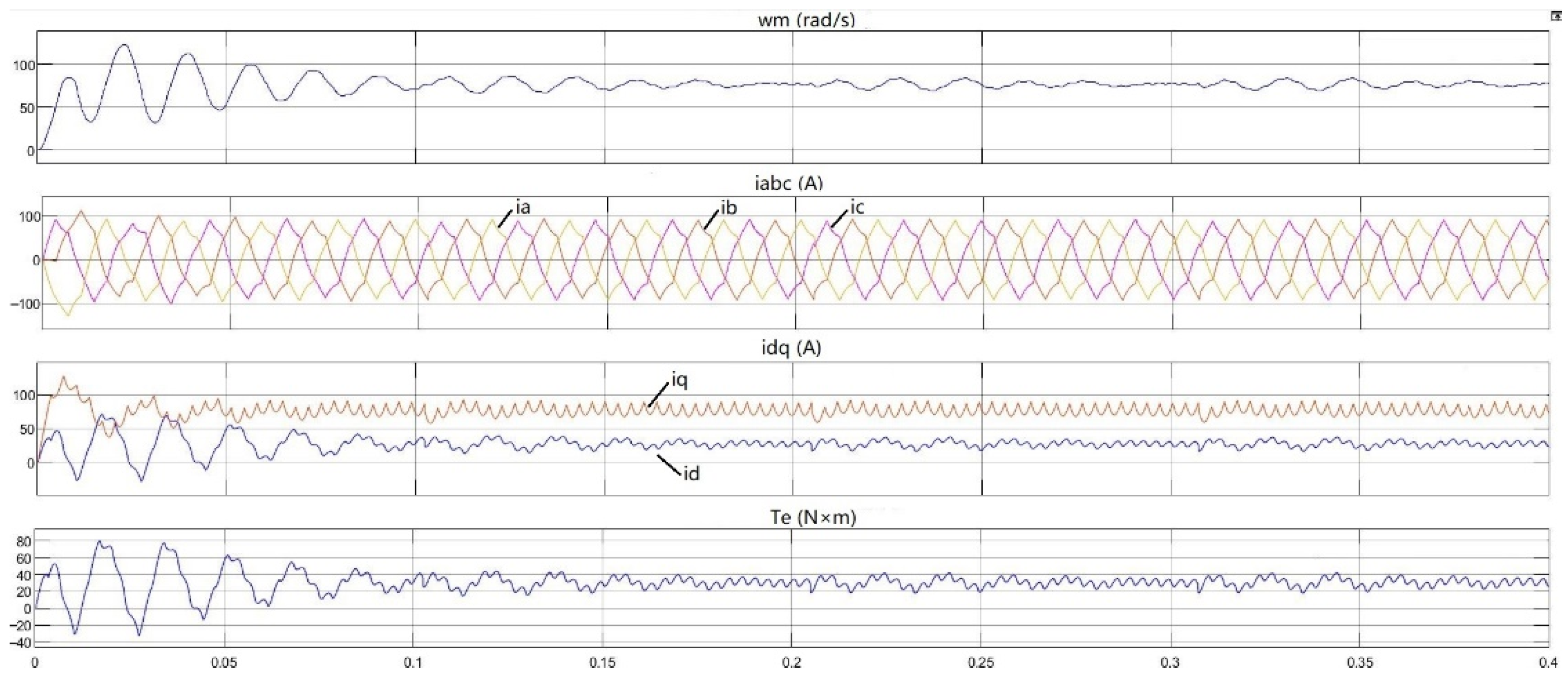
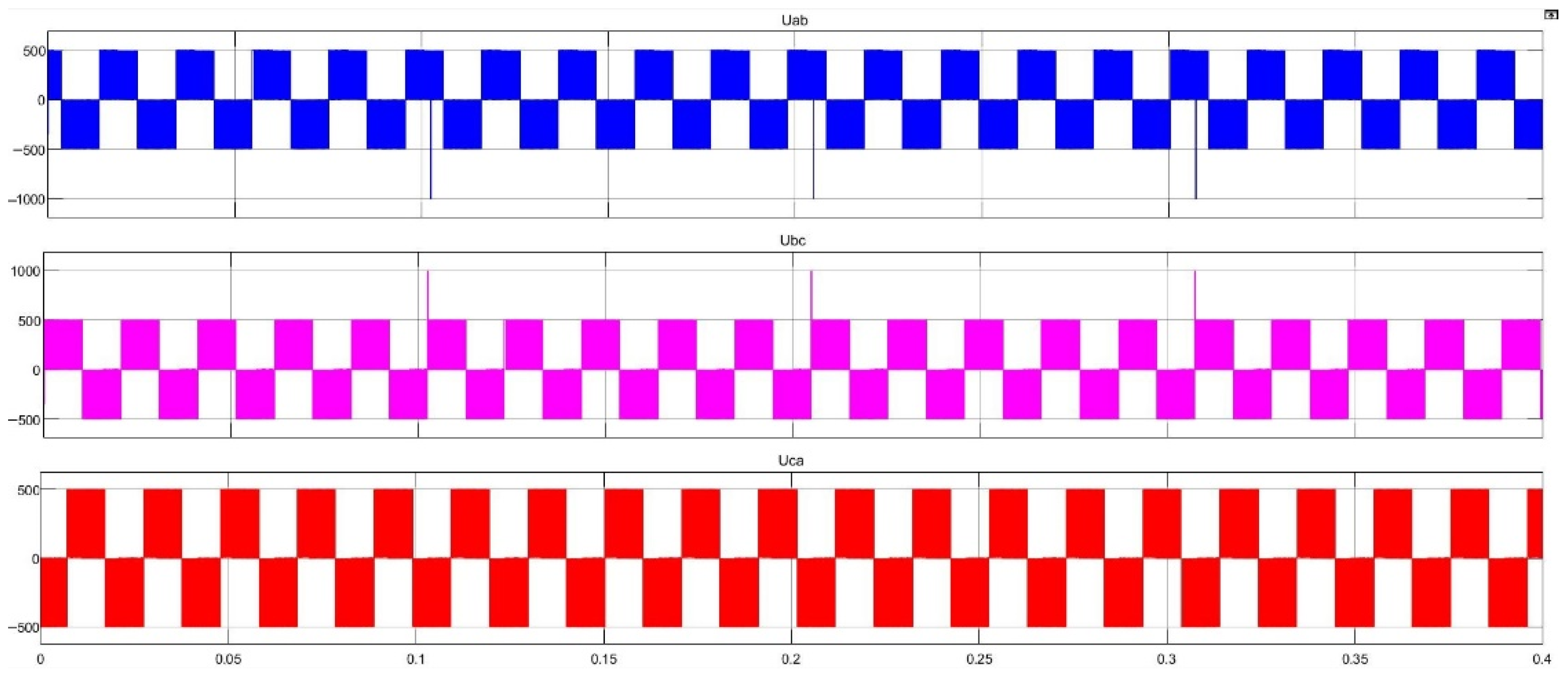
When M = 0.4 , the vector synthesis strategy of 2 × amplitude substitution is equivalent to M = 0.8 , the waveforms of parameter are shown in Figure 9, and the stator phase voltages u ab , u bc and u ca are shown in Figure 10. In Figure 9, the first part is the speed waveform (Unit: rad/s), the second part is the three-phase current ia, ib, ic waveform (Unit: A), the third part is dq current id, iq waveform (Unit: A), the fourth part is torque waveform (Unit: N × m ).
Figure 9. When M = 0.4 , the parameter waveforms of vector synthesis strategy of 2 × amplitude substitution.
Figure 10. When M = 0.4 , the waveforms of stator phase voltages u ab , u bc and u ca in vector synthesis strategy of 2 × amplitude substitution.

4.2. Waveform of Vector Synthesis Algorithm of 1/2 × Amplitude Substitution

When M = 0.4 , the waveforms of the stator phase currents i a , i b and i c in the conventional vector synthesis strategy are shown in Figure 11, and the stator voltages u ab , u bc and u ca are shown in Figure 12. In Figure 11, the first part is the speed waveform (Unit: rad/s), the second part is the three-phase current ia, ib, ic waveform (Unit: A), the third part is dq current id, iq waveform (Unit: A), the fourth part is torque waveform (Unit: N × m ).
Figure 11. When M = 0.4 , the waveforms of parameters of conventional vector synthesis strategy.
Figure 12. When M = 0.4 , the waveforms of stator phase voltages u ab , u bc and u ca in conventional vector synthesis strategy.
When M = 0.8 , the vector synthesis strategy of ½ × amplitude substitution is equivalent to M = 0.4 , the waveforms of parameter are shown in Figure 13, and the stator phase voltages u ab , u bc and u ca are shown in Figure 14. In Figure 13, the first part is the speed waveform (Unit: rad/s), the second part is the three-phase current ia, ib, ic waveform (Unit: A), the third part is dq current id, iq waveform (Unit: A), the fourth part is torque waveform (Unit: N × m ).
Figure 13. When M = 0.8 , the parameter waveforms of vector synthesis strategy of ½ × amplitude substitution.
Figure 14. When M = 0.8 , the waveforms of stator phase voltages u ab , u bc and u ca in vector synthesis strategy of ½ × amplitude substitution.

5. Discussion

Compared with the conventional modulation strategy, the vector synthesis strategy of 2 × amplitude substitution features the synthesis of short vectors, fewer passing areas. The modulation vector is composed of two short vectors and one zero vector, since the composite vector contains zero vector, so it is not necessary to add other zero vector to the seven-segment or five-segment modulation. In the linear region of modulation M [ 0 ,   0.907 ] , the synthesizing vectors can cover the whole hexagon area, the area of hexagonal modulation region is 1.103 times, compared with that of circular modulation region. Furthermore, the synthesis strategy increased in the speed waveform amplitude, but poor waveform of currents i a , i b and i c , as well as over-modulation. In addition, the current amplitudes of three phases are difference, and the NP potential is unbalanced.
In the vector synthesis strategy of 1/2 × amplitude substitution, short vectors are modulated with medium and long vectors, and the current waveform of the three-phase stator is better than that of the vector synthesis strategy of 2 × amplitude substitution, but with more passing areas. In order to further reduce over-modulation, the control algorithm should be added for corrections.
The two optimized modulation strategies feature the reduction of hardware resources and higher simulation speed. By comparison, both modulation algorithms affect the NP balance. To balance the passing areas and waveform quality, the medium and long vector synthesis algorithm of 2 × amplitude substitution is used as the converter modulation algorithm.

6. Conclusions

The principle and four steps of the conventional three-level SVPWM modulation are analyzed. The modulation algorithm of three-level SVPWM sequential synthesis is adopted on this basis. It is not necessary to judge the sector in this algorithm. Instead, only clockwise or counterclockwise rotation based on the angle sequence is required. Adjacent vectors in the area where the reference vector passes need to be synthesized. Then, the vector synthesis algorithm of 2 × amplitude substitution is used. When M ( 0.453 ,   0.907 ] the resultant reference vector changes to M [ 0 ,   0.453 ] , which reduces the switching loss and optimizes the even distribution of heat. Since short vectors are applied and the NP potential unbalance is affected to some extent, the vector synthesis modulation algorithm of 1/2 × amplitude substitution (half of medium and long vectors) is also put forward. Through comparison and analysis, the vector synthesis modulation algorithm of 1/2 × amplitude substitution features high waveform quality, while that of 2 × amplitude substitution features less switching loss, and the 2 × amplitude substitution modulation can cover all hexagon regions, and in the linear region of modulation, the area of modulation area is 1.103 times of the original. The converter of ID-NPC topology is also subjected to simulation experiments by two modulation algorithms, and the feasibility of the improved modulation algorithm is proved.

Author Contributions

Data curation, Y.C.; formal analysis, Y.C.; investigation, X.Z.; methodology, X.Z., Y.C.; project administration, X.Z. All authors have read and agreed to the published version of the manuscript.

Funding

This research was funded by Teaching Research and Reform Program of Cangzhou Jiaotong College, under grant number: HBJY19014.

Conflicts of Interest

The authors declare no conflict of interest.

References

  1. Franquelo, L.G.; Rodriguez, J.; Leon, J.I.; Kouro, S.; Portillo, R.; Prats, M.A. The age of multilevel converters arrives. IEEE Ind. Electron. Mag. 2008, 2, 28–39. [Google Scholar] [CrossRef]
  2. Rodriguez, J.; Bernet, S.; Wu, B. Multilevel Voltage-Source-Converter Topologies for Industrial Medium-Voltage Drives. IEEE Trans. Ind. Electron. 2007, 2930–2945. [Google Scholar] [CrossRef]
  3. Holtz, J.; Oikonomou, N. Neutral Point Potential Balancing Algorithm at Low Modulation Index for Three-Level Inverter Medium-Voltage Drives. IEEE Trans. Ind. Appl. 2007, 43, 761–768. [Google Scholar] [CrossRef]
  4. Zhang, Y.; Li, Y.W.; Zargari, N.R.; Cheng, Z. Improved selective harmonics elimination (SHE) scheme with online harmonic compensation for high-power PWM converters. In Proceedings of the 2014 IEEE Energy Conversion Congress and Exposition (ECCE), Pittsburgh, PA, USA, 14–18 September 2014; pp. 5510–5517. [Google Scholar] [CrossRef]
  5. Celanovic, N.; Boroyevich, D. A comprehensive study of neutral-point voltage balancing problem in three-level neutral-point-clamped voltage source PWM inverters. IEEE Trans. Power Electron. 2000, 15, 242–249. [Google Scholar] [CrossRef]
  6. Gui, S.W.; Wang, L.; Huang, S.H. An Improved VSVPWM Strategy of Considering Neutral-Point Potential Balancing in Three-Level NPC Converter. Appl. Mech. Mater. 2014, 496–500, 1079–1083. [Google Scholar] [CrossRef]
  7. Xia, C.L.; Xu, Z.; Zhao, J.X. A New Direct Power Control Strategy for NPC Three-Level Voltage Source Rectifiers Using a Novel Vector Influence Table Method. J. Power Electron. 2015, 15, 106–115. [Google Scholar] [CrossRef][Green Version]
  8. Zhang, M.S.; Cui, Y.; Wang, Q.J. A Study on Neutral-Point Potential in Three-Level NPC Converters. Energies 2019, 12, 3367. [Google Scholar] [CrossRef]
  9. Seo, J.H.; Choi, C.H.; Hyun, D.-S. A new simplified space-vector PWM method for three-level inverters. IEEE Trans. Power Electron. 2001, 16, 545–550. [Google Scholar] [CrossRef]
  10. Jiang, W.D.; Wang, Q.J.; Chen, Q.; Shi, X.F. SVPWM Strategy for Three-Level Inverter Based on SVPWM Strategy for Two-Level Inverter. Acta Electrotech. Sin. 2009, 24, 108–114. [Google Scholar] [CrossRef]
  11. Cao, Y.l.; Zhang, X.d.; Liu, X. Research on Improved D-NPC Three Phase Three Level Converter and Its Control Strategy. Des. Eng. 2020, 11, 815–823. [Google Scholar] [CrossRef]
  12. Fang, H.; Wu, X.J.; Song, W.S.; Feng, X.Y. Unity Studies Between Three-level SVPWM and CBPWM in the Over-modulation Region. Chin. J. Electr. Eng. 2015, 35, 1994–1996. [Google Scholar] [CrossRef]
  13. Yuan, D.K.; Xu, Y.D.; Li, X.T. Permanent Magnet Synchronous Motor Variable Frequency Speed Regulation System and Its Control; China Machine Press: Beijing, China, 2018; pp. 189–194. [Google Scholar]
  14. Gupta, A.K.; Khambadkone, A.M. A Simple Space Vector PWM Scheme to Operate a Three-Level NPC Inverter at High Modulation Index Including Overmodulation Region, With Neutral Point Balancing. IEEE Trans. Ind. Appl. 2007, 43, 751–760. [Google Scholar] [CrossRef]
  15. Wang, W.; Zhang, B.; Xie, F. A Novel SVPWM for Three-Level NPC Inverter Based on m-Mode Controllability. IEEE Trans. Ind. Electron. 2018, 65, 6055–6065. [Google Scholar] [CrossRef]
  16. Yao, Y.; Kang, L.Y.; Zhang, Z. A Novel Modulation Method for Three-Level Inverter Neutral Point Potential Oscillation Elimination. J. Power Electron. 2018, 18, 445–455. [Google Scholar] [CrossRef]
Publisher’s Note: MDPI stays neutral with regard to jurisdictional claims in published maps and institutional affiliations.

Article Metrics

Citations

Article Access Statistics

Multiple requests from the same IP address are counted as one view.