Article

Floating Body DRAM with Body Raised and Source/Drain Separation

Engineering Department, University of Messina, I-98166 Messina, Italy
Electronics 2021, 10(6), 706; https://doi.org/10.3390/electronics10060706
Submission received: 29 January 2021 / Revised: 13 March 2021 / Accepted: 15 March 2021 / Published: 17 March 2021

Abstract

:
One-Transistor (1T) DRAMs are one of the potential replacements for conventional 1T-1C dynamic memory cells for future scaling of embedded and stand-alone memory architectures. In this work, a scaled (channel length 10nm) floating body 1T memory device architecture with ultra-thin body is studied, which uses a combined approach of a body raised storage region and separated source/drain regions having the role to reduce thermal and field enhanced band-to-band recombination. The physical mechanisms along the geometry and bias scaling are discussed in order to address the requirements of embedded or stand-alone applications. Two-dimensional device simulations show that, with proper optimization of the geometry and bias, the combined approach allows the increase of the retention time and of the programming window by more than one order of magnitude.

1. Introduction

From the early demonstration in 2001 [1], one-Transistor DRAMs (1T-DRAMs) have been largely investigated as a candidate to replace the conventional one transistor-one capacitor (1T-1C) cell. Differently from the 1T-1C architecture, a 1T-DRAM cell is composed of a single device, a Silicon On Insulator MOSFET, which acts with both the roles of access and memory device, leading to superior scaling perspectives with respect to the 1T-1C cell. A different number of 1T-DRAM approaches have been recently reported in the literature [2,3,4,5,6,7]. In Floating Body 1T-DRAMs (FB-DRAMs) [8,9,10,11,12,13,14,15], the information is encoded as non-equilibrium excess charge (typically holes) stored in the bulk of a Silicon On Insulator MOSFET. The advantage of FB-DRAMs with respect to other 1T-DRAM architectures is the higher compatibility with the standard Silicon technology, especially in the cases of embedded systems or systems on chip. In FB-DRAMs, the excess charge is generated by non-equilibrium phenomena like Impaction Ionization (II) and/or Band to Band tunneling (BBT) during the WRITE operation. Due to the body effect, the excess holes stored in the body reduces the threshold voltage, so that a higher channel current is measured during the READ operation. However, the excess charge degrades with time. The retention time of the excess charge is limited by the SRH recombination, during the HOLD operation, in the region where the excess charge is stored. In particular the SRH recombination rate increases with the product of the electron-hole concentrations (np) and reduces with the increase of the recombination lifetime τ. Several new devices, with different materials and/or different architectures, have been proposed to increase the retention time [1,2,3,4,5,6,7,8,9,10,11,12,13,14,15]. In this work we focus on the architectural approach, maintaining the Silicon as the active material. The product np has been reduced by separating the regions where electrons and holes are stored during HOLD operation [12,13,14]. For example, in [13] a body raised region is used to accommodate the excess holes, separating them from the channel electrons. From the other side the lifetime τ has been increased with a low doping in the region where excess charge is stored. In fact, a lower doping increases τ due to a lower band-to-band defect-assisted thermal and field enhanced recombination. A lower doping can be obtained also by separating the high-doped source and drain regions from a low doped channel [15] or using a dopingless channel with Schottky contacts [13]. Another advantage of low doping is a strongly reduced variability induced by random dopant fluctuations. In this work it is proposed a FB-DRAM architecture which uses both concepts of a body raised region and source/drain separation, with particular emphasis on the former, as source/drain separation has been previously discussed by the same author in [15]. It is shown that the combined approach of body raised and source/drain separation can lead to an increase of more than one order of magnitude of the retention time and of the programming window.
The rest of the paper is organized as stated in the following. In Section 2 the proposed device structure is presented, and the details of the simulation model are given. In Section 3 the operation mode during WRITE, ERASE, HOLD and READ operation is discussed with reference to a scaled device geometry with L = 10 nm. In particular, it is discussed how the presence of the body raised region improve the charge holding capability of the memory cell. In Section 4, it is discussed the scaling of the proposed architecture, starting from the scaled geometry discussed in Section 2 (except for the body raised region scaling, which is discussed in Section 3). As geometry scaling has an impact on the necessary bias levels required to obtain given values of retention time and programming window, the optimization of the geometry/bias trade-off is discussed in Section 5. This can serve as a guideline in order to address the requirements of embedded or stand-alone applications. Finally, in Section 6, the summary and conclusions are drawn.

2. Device Structure and Simulation Model

Figure 1 shows a simplified structure of the 1T memory cell under investigation. Source and Drain heavy doped regions (1020 cm−3) are separated from the low doped (1015 cm−3) channel (L = 10 nm) by a spacer region (length LSP) necessary to relax the field in the channel in order to reduce BBT and Trap-Assisted-Tunneling (TAT) to improve the retention time [15]. A raised body region (height WR) is used to accommodate the excess charge during HOLD operation and to relax the field, allowing larger retention time as discussed in the next sections. Technological details about the body raised region can be found in [13]. The equivalent oxide thickness (EOT) is 1 nm, and the Gate workfunction is 4.5 eV (a different workfunction can be immediately considered if the gate voltage is correspondently shifted). Two-dimensional (2D) Atlas device simulation [16] (T = 300 K) are used to investigate the behavior of the proposed architecture. The simulation model includes the drift–diffusion transport model with Fermi–Dirac statistics, concentration-dependent mobility, concentration-dependent lifetime (Scharfetter), SRH generation/recombination and impact ionization (II) (Selberherr). The Hurkx TAT [17] and the non-local BBT models are included in the simulation model with default parameters to reproduce the charge degradation mechanisms in 1T-DRAMs, the first acting for both generation and recombination, the second for generation. However, as will be clear in the next sections, due to large source/drain separation and body raised region height, BBT and TAT are completely turned off in the proposed architecture allowing a larger retention time.
No quantization models are included along the transversal direction due to the large W. In fact, as showed in [18], no significant bandgap widening is present with W = 10 nm and, as discussed in [8], no significant effects on the programming window of FB-DRAMs are observed at this large W.

3. Device Operation

In this section WRITE, ERASE, READ and HOLD operations are discussed with reference to a scaled device geometry with L = LSP = 10 nm and WR = 20 nm. Moreover, the scaling and influence of the body raised region height (WR) are discussed. In Section 4, the scaling of other geometrical/technological parameters are discussed.

3.1. WRITE and ERASE Operations

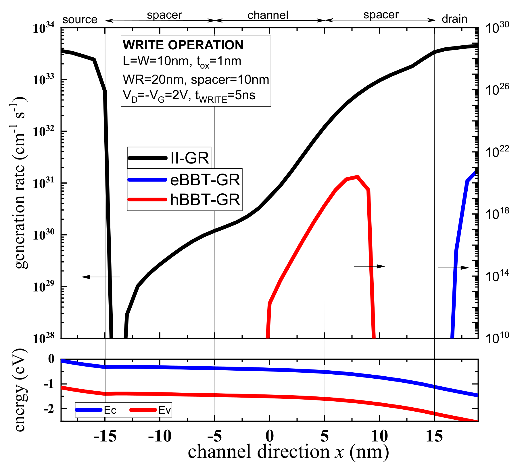
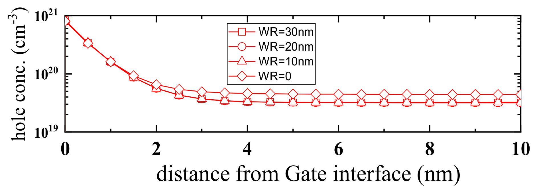
The excess charge is created, during the WRITE operation, via Impact Ionization (II) induced by a sufficient high VD and stored, at the Gate interface, by a sufficient negative VG as discussed in the following. Figure 2 shows a cutline, along the x channel direction (y = 0), of (Top) II and electron/hole BBT generation rates (GR) and (Bottom) conduction and valence bands, at the end of a WRITE operation (pulse width = 5 ns) at the bias VD = −VG = 2 V (the dependence on the pulse strength and width is discussed later). As evident from Figure 2 Top, the overall GR is dominated by II rather than BBT, which is not effective due to the insufficient band-bending at the drain side of the channel and relatively large tunneling distance (Figure 2 Bottom). The low band bending is a consequence of the low doping in the channel region, due to the presence of the spacers, and of the low Gate coupling, due to the presence of the raised region. Impact ionization is mostly localized in the source and drain regions due to the large electric field. The generated excess holes are mainly accumulated at the Gate interface, in the raised region, due to the negative VG during WRITE operation as shown in Figure 3, where a hole concentration cutline along the transversal direction y (x = 0) is shown. Figure 3 shows that the geometry of the raised region (hence its presence) does not affect the charge accumulated during WRITE operation.
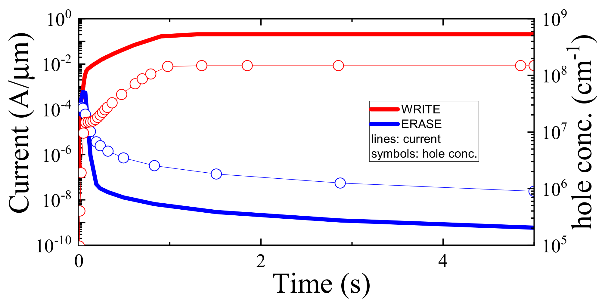
Figure 4 shows the transient behavior of the current (left axis) and of the hole concentration (right axis) during WRITE operation. The hole concentration is integrated in the channel and in the body raised regions (−L/2 ≤ xL/2). Thanks to the very high II-GR (see Figure 2 Top), WRITE operation is very fast so that both the WRITE current and the hole concentration saturate into 1ns (the rise time of the WRITE pulse). Figure 4 shows also the (displacement) current and hole concentration during ERASE operation with VG = VD = 0. As evident, the value of VG = 0 V is sufficiently high in order to quickly increase electron concentration with consequent reduction of excess hole concentration stored in the raised region by SRH recombination [11].
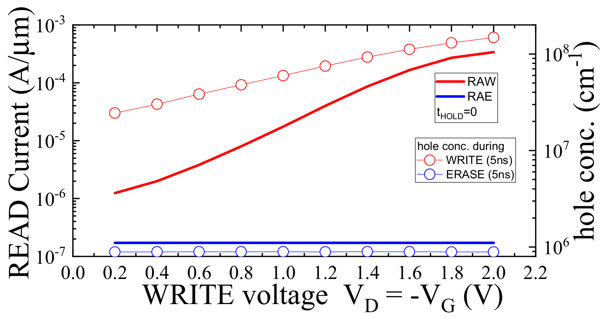
Figure 5 investigates the dependence of the READ current (left-axis) and of integrated hole concentration (right-axis) on the bias VD = −VG during WRITE and ERASE operations. The READ operation immediately follows the WRITE operation (no HOLD operation between) in order to investigate the dependence of the READ after WRITE (RAW) current on the WRITE voltage without the effect of the charge degradation during HOLD operation. The READ current is measured at the end of a pulse width of 5 ns at the bias VG = −2 V, VD = 0.1 V. The hole concentration (red symbols) increases as the WRITE voltage VD = −VG is increased due to the enhanced II-GR (higher VD) and to the higher storage capability at the Gate interface (more negative VG). As consequence, the RAW current increases monotonically with the WRITE bias due to the increasing amount of excess charge. In the same figure, the hole concentration after ERASE and the READ after ERASE (RAE) current, which do not depend on the WRITE bias, are reported to show the memory window. As evident, a large memory window can be obtained also at sub 1V WRITE operation.

3.2. READ Operation

Because READ operations are invasive, the Gate is biased during READ with a sufficient negative voltage, with the aim of retain part of the residual excess charge generated during WRITE operation. Figure 6 shows the electron/hole concentrations (Top) and the energy bands (Bottom) along a cutline in the transversal direction (y), in the middle of the channel (x = 0), at the end of RAW and RAE operations for a READ pulse width tREAD = 5 ns and for a HOLD time tHOLD = 0 (no HOLD operation). Due to the negative Gate bias, the holes generated during WRITE operation (open red symbols in Figure 6 Top) are retained, during RAW operation, in the channel producing an increase, with respect to the case of RAE operation (blue open symbols), of the hole concentration from the Gate interface (maximum increase) to the semiconductor channel region (minimum increase). This increase reflects in energy band lowering (see Figure 6 Bottom) and consequent increase of electron concentration (filled symbols in Figure 6) from the Gate interface (minimum increase) to the channel region (maximum increase). The electron concentration increase reflects in a much higher RAW current with respect to the RAE current (body effect).

3.3. HOLD Operation

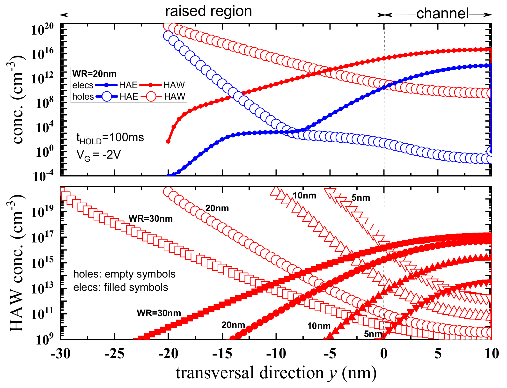
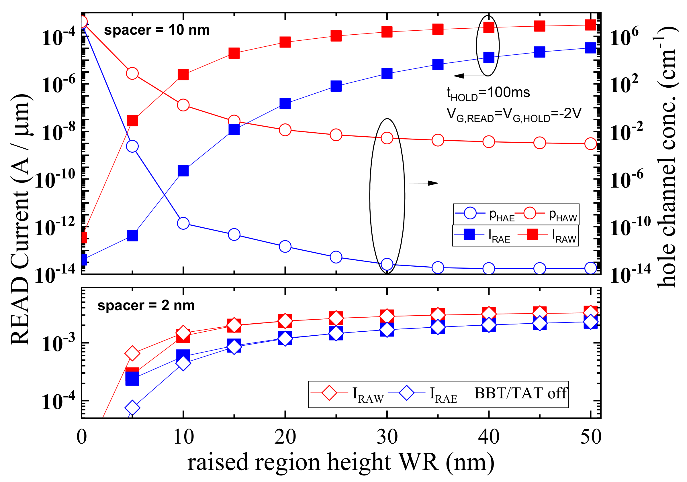
Between WRITE (ERASE) and READ operation, the device is in HOLD mode with vs. = VD = 0 while the gate voltage is sufficient negative in order to maintain as long as possible the charge generated during WRITE operation. Figure 7 shows cutlines, in the y transversal direction (x = 0), of electron and hole concentrations at the end of HOLD after WRITE (HAW) and HOLD after ERASE (HAE) operations at the bias VG = −2 V and with a HOLD time (tHOLD) of 100 ms (>64 ms of the ITRS spec.), for different values of the raised region height WR (WR = 20 nm in Figure 7 Top). Figure 7 shows that, during HOLD, holes are mainly accumulated at the Gate interface, due to the negative Gate voltage (−2 V), while electrons are accumulated mainly at the bottom surface (y = W). This physical separation prevents electron-hole recombination and allows excess charge retention during HAW operation. A higher WR allows a larger volume for excess charge storage and increases the separation of the excess holes from electrons, reducing recombination during HAW. On the other hand, the higher WR produces a lower electrostatic integrity. In fact, the higher WR increases the distance between the Gate and the channel resulting in a reduced capacitive coupling and lower source to channel energy barrier (threshold voltage roll-off). In consequence, in the channel (−L/2 ≤ x ≤ L/2, y ≥ 0), the electron concentration increases, and the hole concentration decreases during HAW/HAE operations (Figure 7 Bottom and Figure 8 Top-right axis). The higher electron concentration increases the RAW/RAE currents, as evident from Figure 8 Top-left axis. The higher HAW hole concentration in the channel with respect to HAE case makes the RAW current (IRAW) higher with respect to the RAE current (IRAE). The increase of the RAW current with WR produces a larger a programming window PW = IRAW − IRAE. However, the reduced hole concentration during HOLD led to a reduced body effect and lower current ratio CR = IRAW/IRAE.
The bottom side of Figure 8 shows the RAW and RAE current with BBT and TAT models turned on (filled symbols) and off (empty symbols) in a geometry with LSP = 2 nm. A smaller spacer is chosen in order to make in evidence the effect of BBT/TAT during HOLD operation. For WR = 5 nm, the charge degradation during HOLD due to BBT/TAT makes the programming window close to zero. However, as WR is increased, the effect of BBT/TAT becomes negligible, and the charge degradation is limited by pure thermal SRH recombination. When the spacer is larger, as for example in Figure 8 Top where LSP = 10 nm, BBT/TAT is already minimized by Source/Drain separation from the channel, and the increase of WR is helpful in increasing the currents, as discussed above. The TAT model used in this work is the well-known Hurkx model (reference [17]), which has only a parameter, the tunneling mass, with a default value of mt = 0.25 × m0. In order to investigate the relevance of this parameter, device simulations by varying mt from 0.1 × m0 to 0.5 × m0 have been done with reference to the geometry WR = 20 nm. The result is that the RAW current varies between 52.2 μA/μm and 58.1 μA/μm while the RAE current varies between 295 nA/μm and 142 nA/μm. As discussed above, this modest variation is due to the fact the TAT model is turned off by the source/drain separation and by the presence of the body raised region. Similar considerations can be derived for the BBT model.
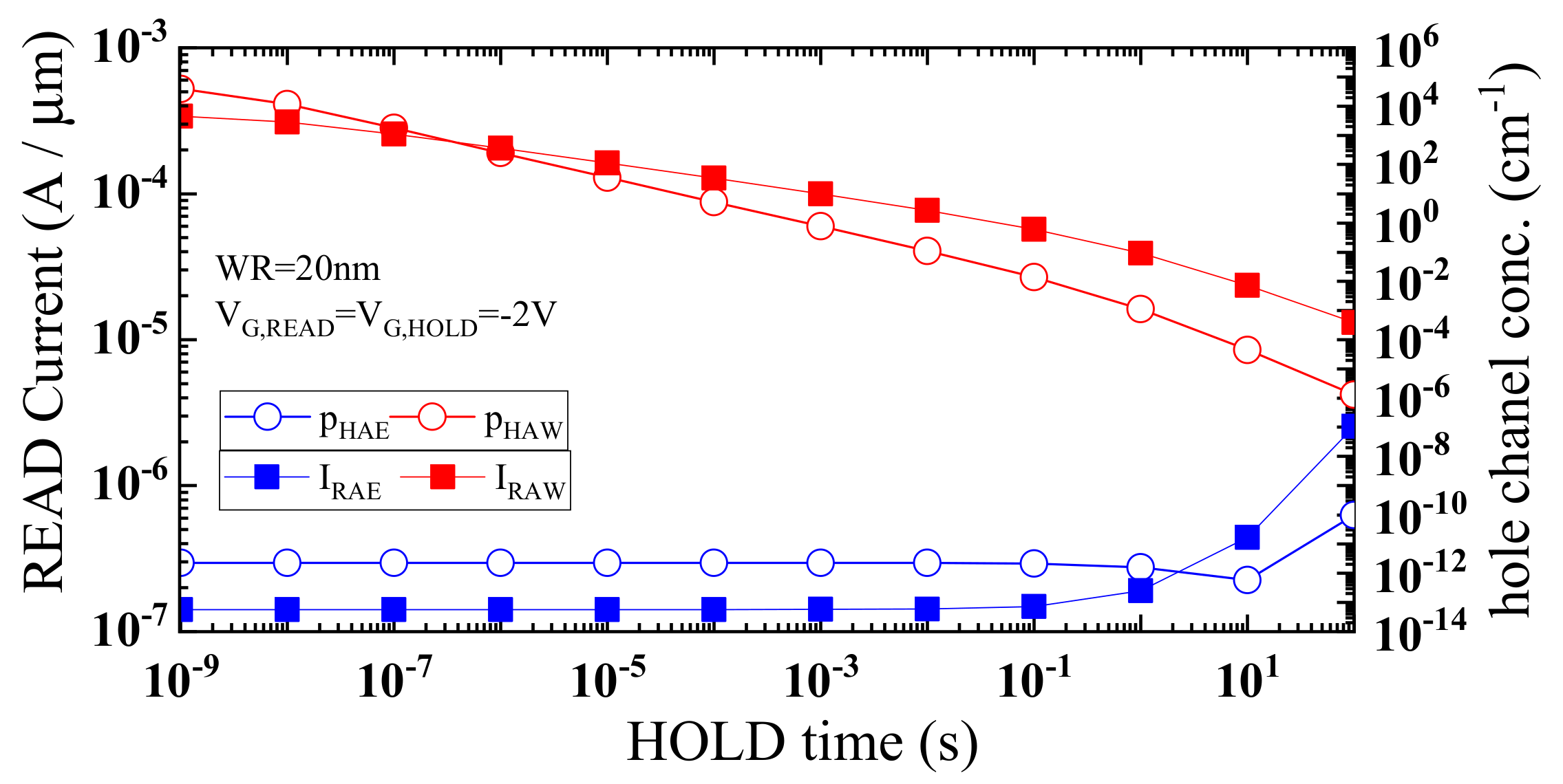
Finally, Figure 9 shows the RAW and RAE currents (filled symbols, left axis) and the integrated hole concentration (empty symbols, right axis) in the channel during HAW and HAE operations as function of the HOLD time. Hole concentration degrades, due to SRH recombination (during HAW) and generation (during HAE), driving the degradation of the RAW and RAE currents. As can be observed, a large memory window (>>6 μA/μm of the ITRS spec.) is obtained at a HOLD time in the order of 10 s.

4. Geometrical and Technological Scaling

Starting from the basic geometry discussed in the previous section (L = LSP = 10 nm, WR = 20 nm, doping 1015 cm−3), in this Section, the geometrical and technological scaling of the proposed device architecture is studied. In particular, data with the BBT and TAT models turned on and off are shown in order to demonstrate the effectiveness of the proposed architecture along the geometrical and technological scaling.
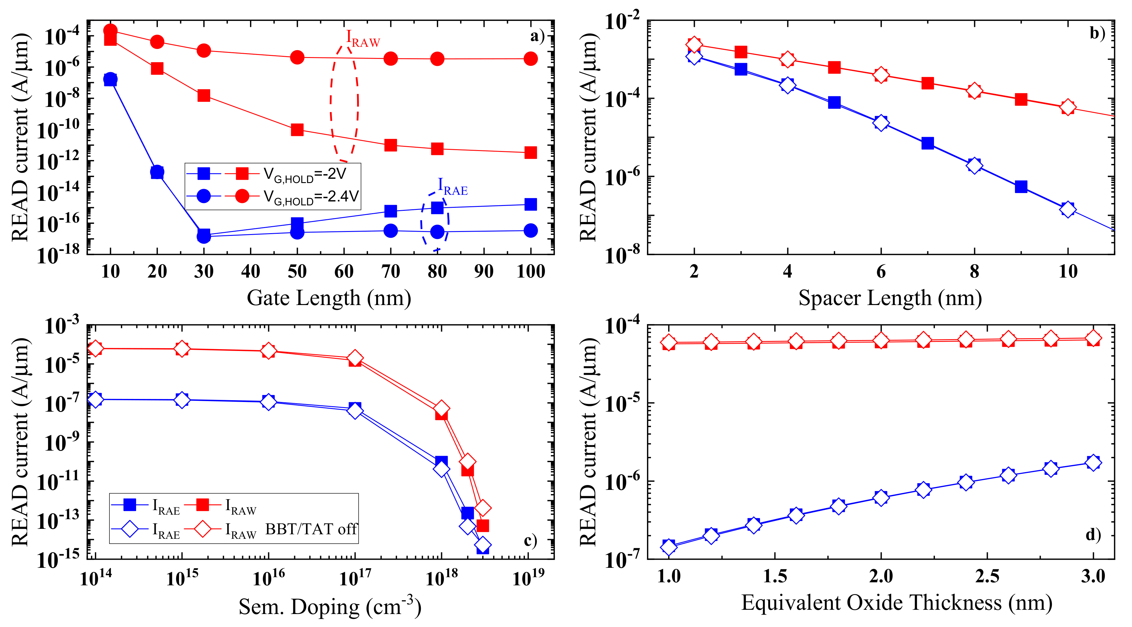
Figure 10a shows the RAW and RAE currents as function of the gate length for two different Gate HOLD biases (VG,HOLD). As L is increased from L = 10 nm, the currents decrease due to the lower channel field and due to the electrostatic improvement. No significant effects of BBT/TAT must be considered due to the large LSP (=10 nm) and WR (=20 nm) as discussed in the previous sections. When VG,HOLD = −2 V (results reported in the previous section), the RAW current drops strongly with L, and the programming window of the case L = 100 nm is much lower with respect to the case L = 10 nm. However, a more negative VG,HOLD (−2.4 V in Figure 10a) can be used to restore the HOLD capability in the longer channels. In this situation, the RAW current reduction is moderate, and it is only due to the lower field in the longer channels, while the RAE current strongly reduces with L due to electrostatic improvement. The result is that the longer channels have a slightly lower programming window with respect to L = 10 nm but a much higher current ratio. Figure 10a shows that the proposed architecture can be scaled towards 10 nm in the Gate length. This is possible only due to the presence of the raised region as shown in Figure 8.
Figure 10b shows the RAW and RAE currents as function of the spacer length (LSP) with BBT/TAT models turned on (filled symbols) and off (empty symbols). As LSP increases, the currents reduce due to the higher series resistance. Source/Drain would relax the field with consequent lower BBT/TAT degradation [15]. However, in Figure 10b WR = 20 nm so that even for small spacer lengths, no significant effect of BBT/TAT degradation is observed.
Figure 10c shows the RAW and RAE currents as function of the semiconductor doping (the doping of the channel, spacers and body raised regions) with BBT/TAT models turned on (filled symbols) and off (empty symbols). In the previous section, the semiconductor doping is set to 1015 cm−3. This corresponds in practice to a low doped or undoped substrate. Figure 10c shows that in a large interval around this value, there is no significant variation of the currents. In fact, at such a low doping level, the low field lifetime is relatively high and the electric field relatively low so that BBT/TAT are irrelevant, and the retention is limited by thermal SRH generation/recombination. As the semiconductor doping is increased above 1016 cm−3, the electrostatic degradation produces a rapidly decrease of the currents and, in any case, a negligible impact of BBT/TAT is observed.
Finally, Figure 10d shows the RAW and RAE currents as function of the EOT. As the EOT is increased, the electrostatic degradation makes the current higher. However, during HAW, the applied bias is able to retain the large excess charge generated during WRITE operation so that the RAW current is less sensitive to the EOT increase.

5. Performance of the Geometry/Bias Trade-Off

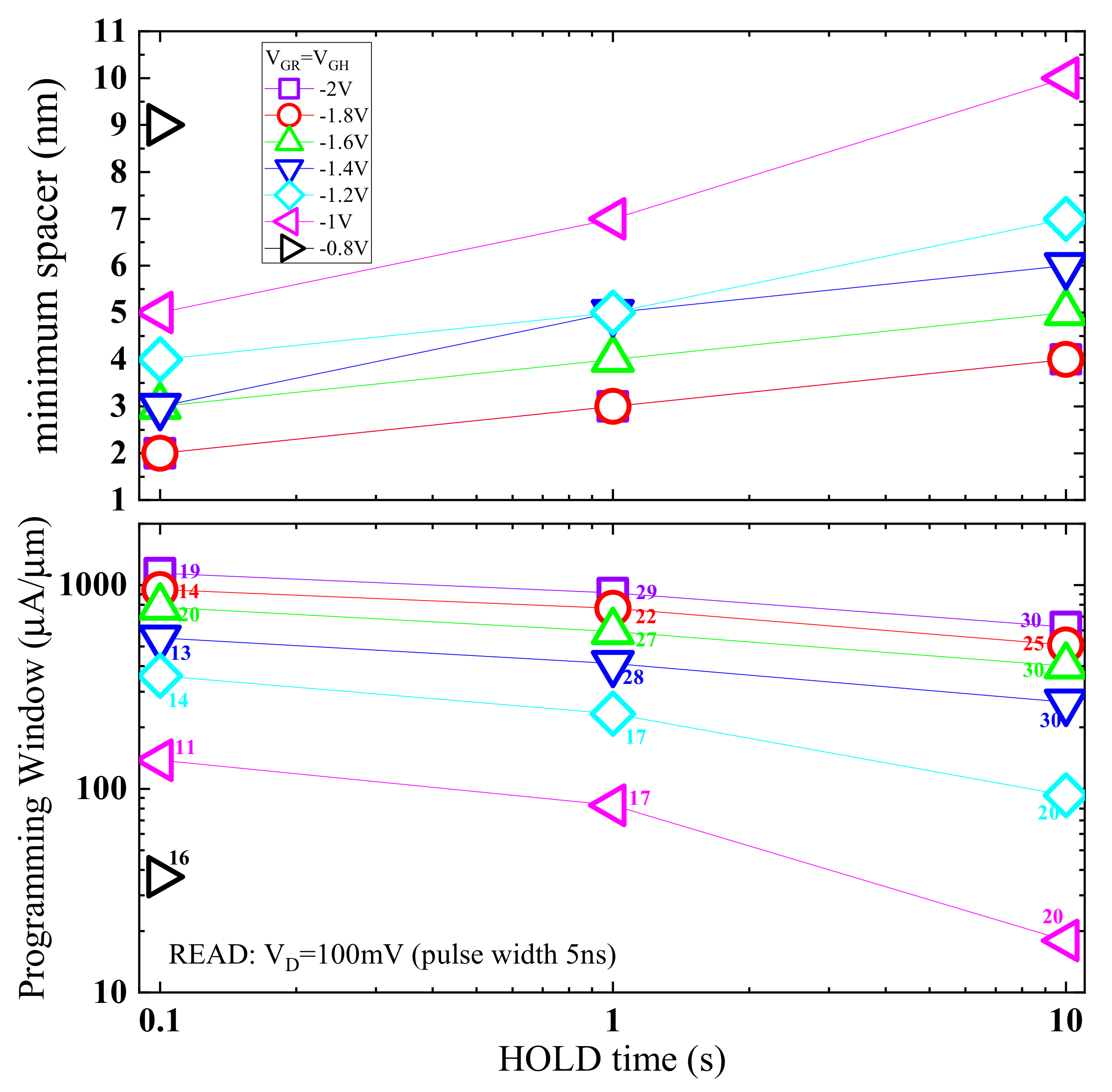
Performances of a 1T-DRAM cell depend on both the geometry and bias. In Figure 11, the PW is studied as function of VG, LSP, WR and of the HOLD time tHOLD. In order to simplify the analysis, we set the same VG during READ and HOLD operations (VG = VG,READ = VG,HOLD) although better performances can be in general obtained with VG,READ ≠ VG,HOLD [11]. As discussed in [11], the more negative is VG, the higher is the HOLD capability and the current ratio, but the lower is the current and the programming window PW. The increase of the spacer length LSP relax the junction field allowing a larger retention time due to the lower TAT recombination. However, the larger series resistance reduces the current and the programming window [15]. Moreover, a larger spacer increases device area. Performances are also a function of the raised region height WR as discussed in the previous section, but differently from the spacer geometry, the raised region height does not affect device area. In particular, the PW increases with WR (Figure 8-left axis) while the current ratio CR reduces. It appears evident that WR cannot be increased as desired, due to the reduction of the CR. In this discussion (and in Figure 11), we limit the minimum current ratio to a value of CR ≥ 2. Figure 10 Top shows, for a given tHOLD and VG, the minimum spacer length necessary to meet ITRS requirements (PW > 6 μA/μm at tHOLD = 64 ms [13]). For each point in Figure 11 Top, the PW and CR are a function of WR. Figure 10 Bottom shows the maximum of the function PW(WR) and the corresponding value of WR close to each symbol. As the required tHOLD is increased, the minimum spacer (hence the device area) needs to be increased to reduce the junction field and TAT recombination (Figure 11 Top). As can be observed, the PW can be maintained relatively large at large tHOLD by using a sufficient height raised region (Figure 11 Bottom). Stated in other words, the reduction of the PW due to the larger LSP can be compensated with a higher raised region. This approach allows maintaining a relatively high PW also at higher tHOLD. The value of the gate voltage VG is important as well as the geometry. In fact, in embedded or system on chip applications, the bias is often limited by the logic circuitry, while in stand-alone memory chips applications, it can be relaxed in the limits of the maximum allowed power consumption. As can be observed in Figure 11 Top, the minimum LSP, hence the device area, can be reduced if a more negative VG is allowed. In fact, the higher HOLD capability due to the more negative VG compensates the higher TAT degradation due to the lower LSP. Moreover, the more negative can be VG, the higher can be WR, due to the reduced gate coupling, allowing a larger programming window (Figure 11 Bottom). The performance of a DRAM cell can be discussed in terms of the programming window, guaranteeing a retention time of at least 64 ms from the ITRS specification, or in terms of retention time, guaranteeing a programming window of at least 6 μA/μm of the ITRS specification [13]. Following the first point of view, it is evident from Figure 11 that with tHOLD = 100 ms (>64 ms of the ITRS spec.), the PW can reach 100 μA/μm (>>6 μA/μm of the ITRS spec.) with |VG| limited to 1V and LSP = 5 nm, while it can be large up to 1 mA/μm if |VG| can be pushed down to 2 V maintaining a short spacer (2 nm). However, from the other point of view, 10 s of retention time can be obtained with LSP = 10 nm with |VG| limited to 1 V while device area can be reduced with LSP = 4 nm if |VG| can be pushed down to 2 V.

6. Conclusions

In this work, the physics and geometry/bias trade-off of a scaled (L = 10 nm) device memory cell architecture with a body raised region and source/drain separation spacers is studied, concepts already proposed independently of each other. Source and drain separation spacers reduce the electric field in the active region of the device with consequent reduction of BBT/TAT degradation, but with a reduction of the channel current and of the programming window due to the higher series resistance. On the other hand, the body raised region stores the excess charge during device operation separating it from the conduction charge flow with consequent reduction of the field and thermal SRH recombination, inducing higher retention time and programming window. The raised body is therefore used to balance the current reduction due to the spacers, without affecting device area. Moreover, the body raised region switches off BBT and TAT as source/drain separation. The geometrical and technological scaling is influenced only by electrostatic degradation as BBT/TAT are switched off by the spacers and by the body raised region. The performances of the memory cell depend on a trade-off between geometry and bias. In particular, the trade-off between the body raised region height (WR), the spacers length (LSP) and the gate bias (VG) is studied, as reported in Figure 11. While WR can be increased without affecting device area, LSP and |VG| require to be minimized for future scaled technologies. It is evident that the combined approach of body raised and source/drain separation regions is able to increase the retention time or the programming window by more than one order of magnitude in order to address the requirements of embedded or stand-alone applications.

Funding

This research received no external funding.

Conflicts of Interest

The authors declare no conflict of interest.

References

  1. Okhonin, S.; Nagoga, M.; Sallese, J.M.; Fazan, P. A SOI capacitor-less 1T-DRAM concept. In Proceedings of the International SOI Conference, Durango, CO, USA, 1–4 October 2001; pp. 153–154. [Google Scholar]
  2. Shin, J.S.; Choi, H.; Bae, H.; Jang, J.; Yun, D.; Hong, E.; Kim, D.H.; Kim, D.M. Vertical-Gate Si/SiGe Double-HBT-Based Capacitorless 1T DRAM Cell for Extended Retention Time at Low Latch Voltage. IEEE Electron Device Lett. 2012, 33, 134–136. [Google Scholar] [CrossRef]
  3. Moon, D.-I.; Kim, J.-Y.; Moon, J.-B.; Kim, D.-O.; Choi, Y.-K. Evolution of Unified-RAM: 1T-DRAM and BE-SONOS Built on a Highly Scaled Vertical Channel. IEEE Trans. Electron Devices 2014, 61, 60–65. [Google Scholar] [CrossRef]
  4. Navlakha, N.; Lin, J.-T.; Kranti, A. Retention and Scalability Perspective of Sub-100-nm Double Gate Tunnel FET DRAM. IEEE Trans. Electron Devices 2017, 64, 1561–1567. [Google Scholar] [CrossRef]
  5. Yoon, Y.J.; Seo, J.H.; Cho, S.; Lee, J.-H.; Kang, I.M. A polycrystalline-silicon dual-gate MOSFETbased 1T-DRAM using grain boundaryinduced variable resistance. Appl. Phys. Lett. 2019, 114, 183503. [Google Scholar] [CrossRef]
  6. Cristoloveanu, S.; Lee, K.H.; Parihar, M.S.; El Dirani, H.; Lacord, J.; Martinie, S.; Le Royer, C.; Barbe, J.-C.; Mescot, X.; Fonteneau, P.; et al. A review of the Z2-FET 1T-DRAM memory: Operation mechanisms and key parameters. Solid State Electron. 2018, 143, 10–19. [Google Scholar] [CrossRef] [Green Version]
  7. Navarro, C.; Karg, S.; Marquez, C.; Navarro, S.; Convertino, C.; Zota, C.; Czornomaz, L.; Gamiz, F. Capacitor-less dynamic random access memory based on a III–V transistor with a gate length of 14 nm. Nat. Electron. 2019, 2, 412–419. [Google Scholar] [CrossRef]
  8. Butt, N.Z.; Alam, M. Scaling limit of double-gate and surround-gate Z-RAM cells. IEEE Trans. Electron Devices 2007, 54, 2255–2261. [Google Scholar] [CrossRef]
  9. Giusi, G.; Alam, M.A.; Crupi, F.; Pierro, S. Bipolar Mode Operation and Scalability of Double Gate Capacitorless 1T DRAM Cells. IEEE Trans. Electron Devices 2010, 57, 1743–1750. [Google Scholar] [CrossRef]
  10. Giusi, G. Investigation on junctionless floating body DRAMs including Trap Assisted Tunneling. Solid State Electron. 2020, 169, 107799. [Google Scholar] [CrossRef]
  11. Giusi, G. Physical insights of body effect and charge degradation in floating-body DRAMs. Solid State Electron. 2014, 95, 1–7. [Google Scholar] [CrossRef]
  12. Kim, G.; Kim, S.W.; Song, J.Y.; Kim, J.P.; Ryoo, K.-C.; Oh, J.-H.; Park, J.H.; Kim, H.W.; Park, B.-G. Body-Raised Double-Gate Structure for 1T DRAM. In Proceedings of the 2009 IEEE Nanotechnology Materials and Devices Conference, Traverse City, MI, USA, 2–5 June 2009. [Google Scholar]
  13. Lin, J.-T.; Sun, W.-T.; Lin, H.-H.; Chen, Y.-J.; Navlakha, N.; Kranti, A. Raised Body Doping-Less 1T-DRAM With Source/Drain Schottky Contact. IEEE J. Electron Devices Soc. 2019, 7, 276–281. [Google Scholar] [CrossRef]
  14. Ansari, H.R.; Navlakha, N.; Lee, J.Y.; Cho, S. Double-Gate Junctionless 1T DRAM With Physical Barriers for Retention Improvement. IEEE Trans. Electron Devices 2020, 67, 1471–1479. [Google Scholar] [CrossRef]
  15. Giusi, G.; Iannaccone, G. Junction Engineering of 1T-DRAMs. IEEE Electron Device Lett. 2013, 34, 408–410. [Google Scholar] [CrossRef]
  16. Available online: https://www.silvaco.com/products/tcad/device_simulation/atlas/atlas.html (accessed on 29 January 2021).
  17. Hurkx, G.A.M.; Klaassen, D.B.M.; Knuvers, M.P.G. A New Recombination Model for Device Simulation Including Tunneling. IEEE Trans. Electron Devices 1992, 39, 331–338. [Google Scholar] [CrossRef]
  18. Gundapaneni, S.; Bajaj, M.; Pandey, R.K.; Murali, K.V.R.M.; Ganguly, S.; Kottantharayil, A. Effect of Band-to-Band Tunneling on Junctionless Transistors. IEEE Trans. Electron Devices 2012, 59, 1023–1029. [Google Scholar] [CrossRef]
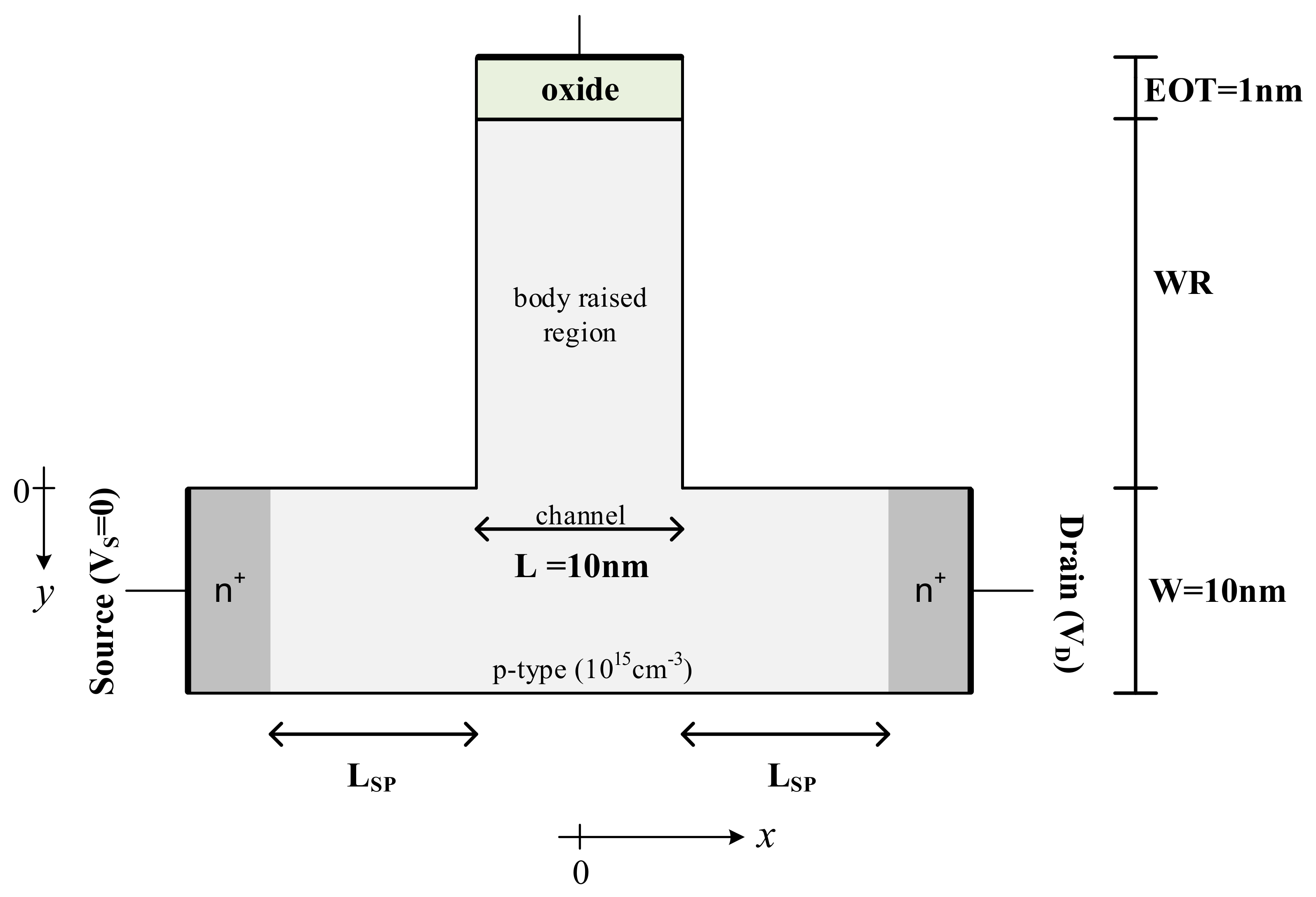
Figure 1. The simulated device structure: source/drain are separated from the low doped channel region (length L, thickness W) by a spacer region (length LSP). A raised body region (height WR) is used to accommodate excess charge during HOLD operation.
Electronics 10 00706 g001
Figure 2. Cutline, along the x channel direction (y = 0), of (Top) Impact Ionization and electron/hole Band to Band tunneling (BBT) generation rates and (Bottom) conduction and valence bands, at the end of a WRITE operation at the bias VD = −VG = 2 V (pulse width = 5 ns).
Electronics 10 00706 g002
Figure 3. Cutline of the hole concentration along the transversal direction y (x = 0) at the end of a WRITE operation (tWRITE = 5 ns) at the bias VD = −VG = 2 V.
Electronics 10 00706 g003
Figure 4. (left axis) current and (right axis) hole concentration during WRITE (VD = −VG = 2 V) and ERASE (VG = VD = 0) operations. The hole concentration is integrated in the channel and in the body raised region (−L/2 ≤ xL/2).
Electronics 10 00706 g004
Figure 5. (left axis) READ after WRITE (RAW) and READ after ERASE (RAE) currents (tHOLD = 0, VG = −2 V, VD = 0.1 V) and (right axis) the integrated hole concentration during WRITE and ERASE operations as function of the WRITE voltage VD = −VG (VG = VD = 0 during ERASE). The hole concentration is integrated in the channel and in the body raised region (−L/2 ≤ xL/2).
Electronics 10 00706 g005
Figure 6. Cutlines in the y direction at the center of the device (x = 0) of (Top) electron and hole concentrations and (Bottom) energy bands at the end of RAE/RAW operations. The bias point is VG,READ = −2 V, with tREAD = 5 ns and tHOLD = 0.
Electronics 10 00706 g006
Figure 7. Cutlines in the y transversal direction (x = 0) of electron and hole concentrations at the end of (Top) HOLD after ERASE (HAE)/HOLD after WRITE (HAW) operations for WR = 20 nm and (Bottom) for varying WR at the end of the HAW operation. The Gate bias is VG = −2 V and the HOLD time tHOLD = 100 ms.
Electronics 10 00706 g007
Figure 8. (Top-left axis) RAW and RAE currents and (Top-right axis) integrated hole concentration in the channel region (−L/2 ≤ xL/2, y ≥ 0) during HAW and HAE as function of the raised region height (WR). At the bottom are shown the RAW and RAE currents with BBT and Trap-Assisted-Tunneling (TAT) models turned on (filled symbols) and off (empty symbols) in a geometry with LSP = 2 nm.
Electronics 10 00706 g008
Figure 9. (left axis) RAW and RAE currents and (right axis) integrated hole concentration in the channel during HAW and HAE as function of the HOLD time. The hole concentration is integrated in the channel and in the body raised region (−L/2 ≤ xL/2, y ≥ 0).
Electronics 10 00706 g009
Figure 10. RAW and RAE currents, at tHOLD = 100 ms and VG,READ = −2 V, VG,HOLD = −2 V, as function of (a) gate length L; (b) spacer length LSP; (c) semiconductor doping; and (d) equivalent oxide thickness (EOT). Parameters vary around the geometry discussed in Section 3 (L = W = LSP = 10 nm, WR = 20 nm).
Electronics 10 00706 g010
Figure 11. (Top) Minimum spacer length in order to meet ITRS requirements as function of tHOLD and VG,READ = VG,HOLD; (Bottom) the corresponding programming window (close to each symbol the corresponding value of the optimum WR). The observation spaces for LSP and WR are limited to 10 nm and 50 nm, respectively, with 1 nm resolution.
Electronics 10 00706 g011
Publisher’s Note: MDPI stays neutral with regard to jurisdictional claims in published maps and institutional affiliations.