Article

Reconfiguration Strategy for Fault Tolerance in a Cascaded Multilevel Inverter Using a Z-Source Converter

by
Jesus Aguayo-Alquicira
1,
Iván Vásquez-Libreros
1,
Susana Estefany De Léon-Aldaco
1,*,
Mario Ponce-Silva
1,
Ricardo Eliu Lozoya-Ponce
2,
Eligio Flores-Rodríguez
3,
Jarniel García-Morales
1,
Yesenia Reyes-Severiano
1,
Luis Mauricio Carrillo-Santos
1,
Manuel Marín-Reyes
1 and
Eider Miguel Amores-Campos
1
1
Tecnológico Nacional de México-CENIDET, Cuernavaca 62490, Mexico
2
Tecnológico Nacional de México-Instituto Tecnológico de Chihuahua, Chihuahua 31310, Mexico
3
Tecnológico Nacional de México-Instituto Tecnológico Superior de Los Reyes, Los Reyes 60300, Mexico
*
Author to whom correspondence should be addressed.
Electronics 2021, 10(5), 574; https://doi.org/10.3390/electronics10050574
Submission received: 5 February 2021 / Revised: 26 February 2021 / Accepted: 26 February 2021 / Published: 1 March 2021
(This article belongs to the Section Power Electronics)

Abstract

:
The cascade multilevel inverters are widely used in industrial manufacturing processes for DC-AC conversion. Therefore, the reliability and efficiency improvement, optimized control, and fault-tolerant strategies are areas of interest for researchers. The fault tolerance strategies applied to cascade multilevel inverters are classified as material redundancy and analytical redundancy. This paper presents the use of the Z-source converter as a fault reconfiguration method applied to a cascade multilevel inverter. On the one hand, the proposed approach has the characteristic of combining the use of material redundancy (modifying the output voltage by changing the Z-source operation), and on the other hand, it has the use of analytical redundancy (modifying the switching sequence of the multilevel inverter, changing from symmetrical to asymmetrical operation mode). This approach has been validated by experimental results of the system under fault-free conditions and employing the Z-source converter as the main fault reconfiguration element. The proposed fault reconfiguration strategy allows the cascaded multilevel inverter to continue to operate even in the presence of a fault by having continuous operation.

1. Introduction

The cascade multilevel inverters (CMLI) are widely used in industrial manufacturing processes for DC-AC conversion for several advantages compared to a two-level inverter, such as including the ability to higher voltage stress due to their cascaded structure, lower common-mode voltage, and lower Total Harmonic Distortion (THD) [1]. Among the disadvantages of the CMLI are complex control strategies and a larger number of semiconductor devices. The increased number of power semiconductor devices in CMLI increases the risk of failures, since the failure of a single device could cause the whole inverter to fail.
The most usual faults that may occur in the CMLI are open- and short-circuit faults in power semiconductor devices as well as the loss of gate pulse signals (control failure) such as those shown in Figure 1 [2]. The control failure could be considered as an open-circuit fault in the power semiconductor devices and thus, the main faults are open- and short-circuit faults.
If an open-circuit fault occurs in the CMLI, the loss of one or several voltage levels could occur. If a short-circuit fault happens, the short circuit circulation path could cause extra electrical stress on the power semiconductor devices (thermal fatigue) or a short-circuit condition on the source side, which results in further damage [3,4].
When a fault occurs in the CMLI, the failed component should be diagnosed and located for possible recovery. However, the large variety of power converter topologies and structures, as well as a large number of power semiconductor devices in the CMLI, could cause ambiguous conditions that impede the fault diagnosis. This issue has attracted significant research interest to yield effective fault-tolerant strategies. To detect the faults in the CMLI, various fault diagnostic methods have been developed [5,6].
The fault tolerance strategies applied to CMLI are classified as material redundancy and analytical redundancy, and they are briefly described below.

1.1. Material Redundancy

This type of redundancy involves having extra elements to replace the damaged elements. Making use of this redundancy allows systems to isolate the fault and continue to operate in degraded conditions. In references [7,8,9], material redundancy is used by connecting an auxiliary branch in parallel to the converter; when a short-circuit fault occurs in any of the circuit breakers, this auxiliary branch is activated, replacing the damaged branch. Similarly, in reference [10], bidirectional switches are used on each cell of the CMLI, which are directly connected to transformers with a different ratio in each of their windings.
For material redundancy, it is necessary to use high-speed electronic devices to detect and replace the damaged branch. Therefore, it is necessary to have efficient sensing systems, since an unbalance in the sensed voltages can cause the disconnection of one or more elements in a fault-free condition.

1.2. Analytical Redundancy

Analytical redundancy is also referred to as software redundancy. It consists of the incorporation of an additional block in the control system capable of reconfiguring the output signals of the system using feedback of these signals [11]. Employing this type of redundancy allows the system to continue to operate even after a fault has occurred, operating with degradation in its output signals without adding extra devices to the system circuitry, reflecting a decrease in its implementation costs [12].
In reference [13], the PWM signal re-assignment technique is used in the CMLI; this strategy bases its operating principle on the comparison of high-frequency carrier signals with a low-frequency modulating signal generating switching pulses that control the full-bridge switches of the CMLI. The modularity characteristic of these systems is used to perform a re-accommodation of their control signals even after a failure of one of the cells of the complete bridge.
This paper presents the use of the Z-source converter as a fault reconfiguration method applied to a CMLI. The proposed approach combines the modification of the output voltage due to a change in the Z-source converter operation, and it modifies the switching sequence of the multilevel inverter, allowing the change from symmetrical to an asymmetrical operation mode. The proposed fault reconfiguration strategy in this paper allows the CMLI to remain in operation even in the presence of a fault in any cell of the CMLI (only one fault at a time). In addition, the THD value obtained is within the values established in the IEEE 519 standard.
The rest of the paper is organized as follows: Section 2 presents the description of the cascaded multilevel inverter. Section 3 describes the design equations of the Z-source converter, as well as the two operating states. Subsequently, Section 4 presents the description of the proposed reconfiguration technique. Section 5 shows the experimental results obtained from the behavior of the cascaded multilevel inverter without faults and with faults by applying the proposed method. Finally, the conclusions of this document are found in Section 6.

2. Multilevel Inverter

The main function of the CMLI is to synthesize the output AC voltage from a DC voltage level at the input, which can be connected in series or cascade, summing the voltages. CMLI includes an array of power semiconductor devices and capacitor or DC voltage sources that generate step-waveform output voltages. Multilevel technology started with the three-level converter; then, it was followed by numerous multilevel inverter topologies. By increasing the number of levels in the inverter, the output voltage has more steps generating a staircase waveform, which has a reduced THD value. However, a high number of levels increases the control complexity and introduces voltage unbalance problems [14].
The CMLI depending on the power supply can be symmetrical or asymmetrical.

2.1. Symmetrical Cascaded Multilevel Inverter (S-CMLI)

The symmetrical CMLI (S-CMLI) consists of “S” cells connected in series, which are powered by isolated DC sources. Their number of levels is defined by the following equation:
L = 2 S + 1
where L is the number of output voltage levels and S is the number of H-bridge cells with their respective DC source.
Figure 2 shows the CMLI for three H-bridge cells and seven-level output voltage.

2.2. Asymmetrical Cascaded Multilevel Inverter (A-CMLI)

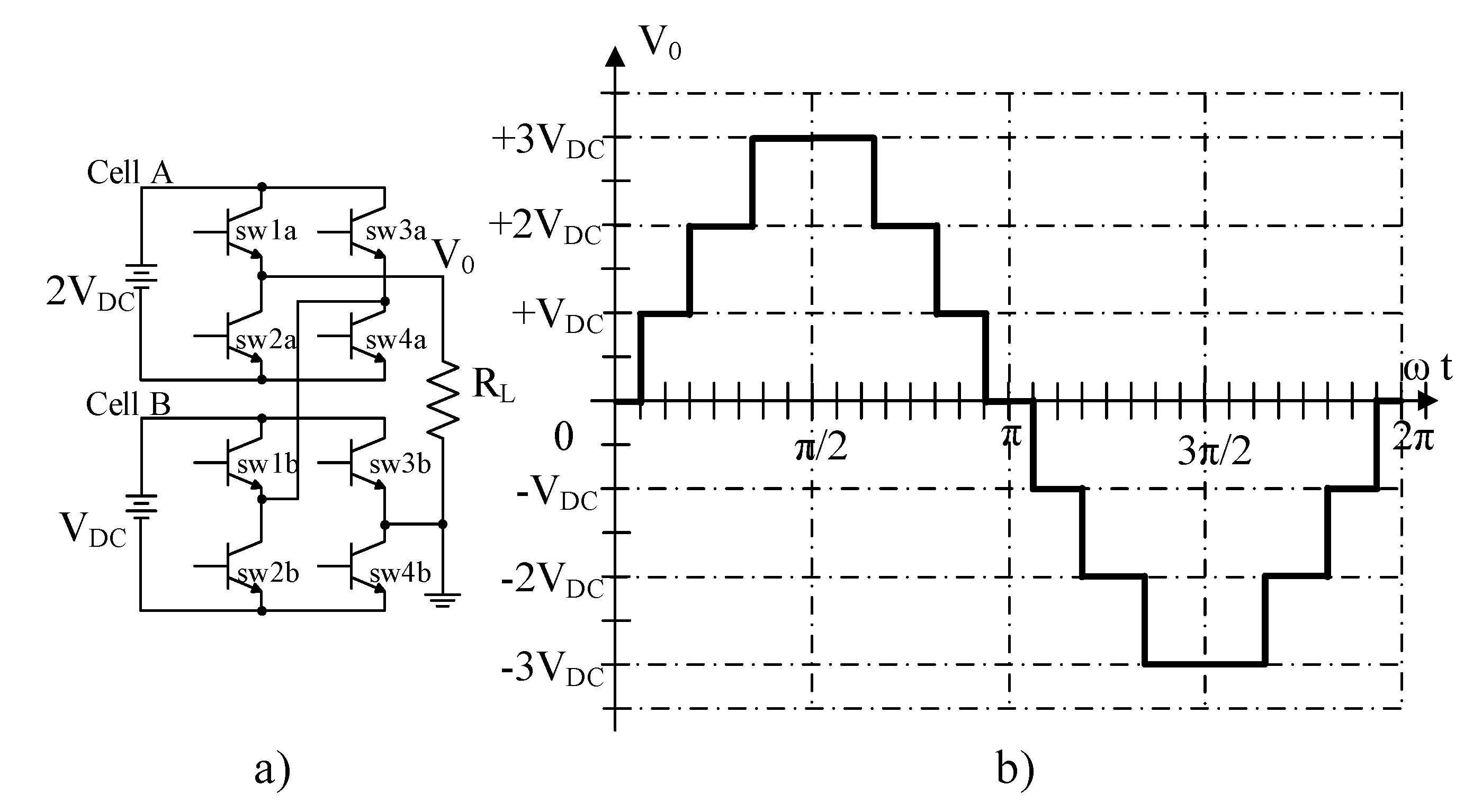
The asymmetrical CMLI (A-CMLI) is a modification of the conventional topology of the multilevel inverter (S-CMLI), being differentiated only by the voltage ratio applied to the power supplies of each of the cells. A-CMLI generates more levels in the output waveform with fewer cells compared to other multilevel topologies [15]. There are two A-CMLI structures: (a) Binary (power of 2) in which the supply voltage of each cell is doubled consecutively, and (b) Trinary (power of 3) in which the supply voltage of each cell is tripled consecutively [16] and [17].
L = 2 s + 1 1
where L is the number of output voltage levels and S is the number of H-bridge cells with their respective DC source.
Figure 3 shows the A-CMLI for two H-bridge cells and a seven-level output voltage. Comparing Figure 2b and Figure 3b, seven levels of the output voltage waveform are observed for both cases: three cells (symmetrical) and two cells (asymmetrical). This is possible only by making modifications to the switching sequence of the cells and duplicating the supply voltage of one of the cells. The above describes the main idea of the reconfiguration technique when a fault occurs in one of the cells that compose the CMLI.

3. Z-source Inverter

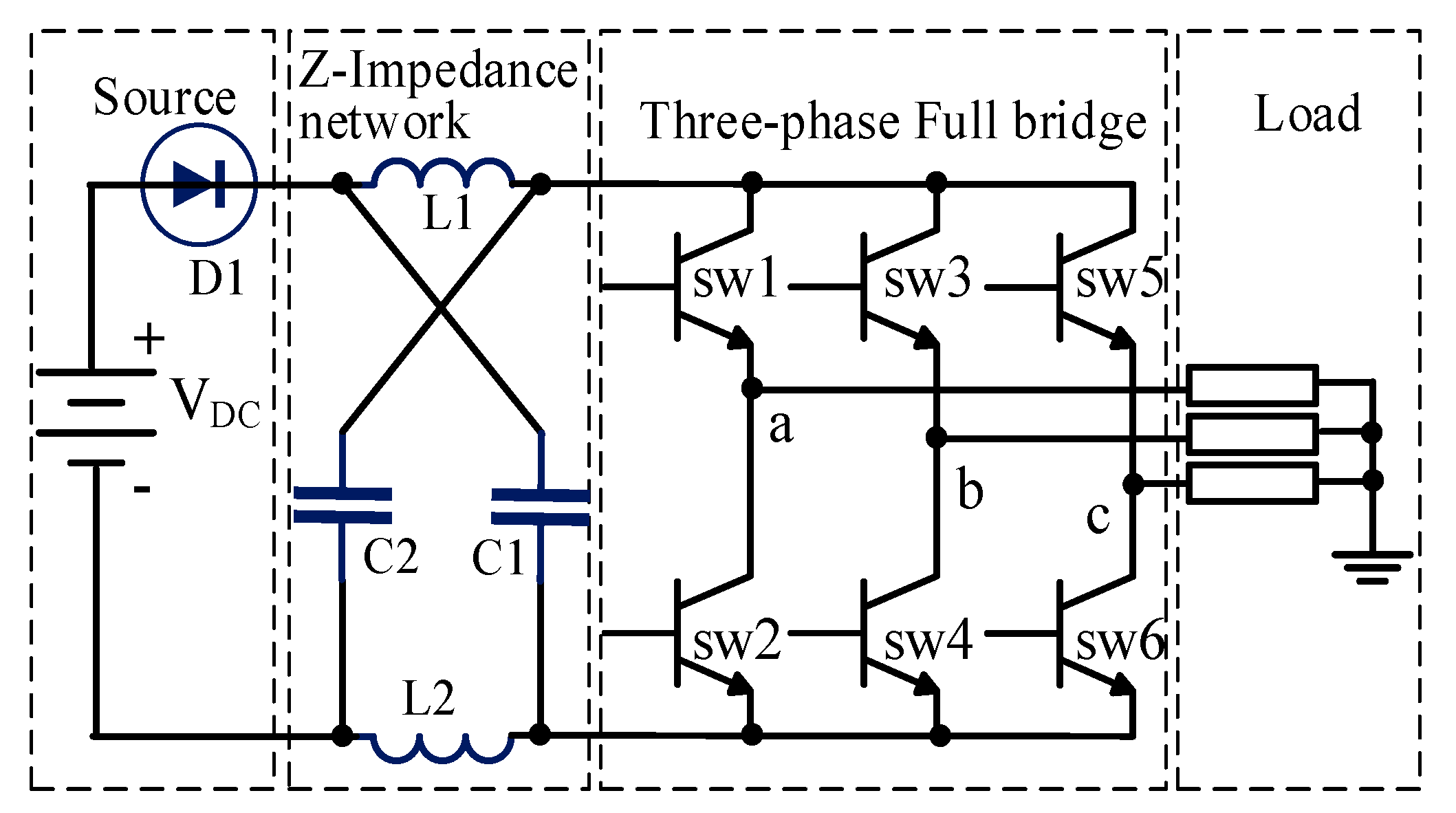
The Z-source inverter (ZSI) also known as the Z-impedance network, emerged as a DC-AC power converter in 2002 introduced by Peng [18]. The ZSI in conjunction with the three-phase bridge configuration type [19] allows the inverter to increase the output voltage using only one conversion stage, as shown in Figure 4.
The ZSI uses an impedance network at the input consisting of the inductors (L1 and L2) and the capacitors (C1 and C2), as shown in Figure 4. The capacitors are connected diagonally, and in conjunction with the inductors, they form a second-order filter that operates as energy storage. This allows increasing the voltage with an optimal design using components with low capacitance and inductance values, reducing the implementation cost [20].
The operating principle of ZSI depends on the switching states of the inverter connected to it.

3.1. Z-Source Converter

We replace the three-phase full-bridge of the Z-source inverter (shown in Figure 4) with a switch named Q1, which is controlled by the trigger signal “D” generated by the “Simple Boost” method. Therefore, the Z source is used as a DC-DC converter switched to high frequency and with increased dynamic speed. Figure 5 shows the simplified diagram of the Z-source converter.
The Z-source converter, similar to the ZSI, operates on the same principles as the NST (Non-Shoot-Through) and ST (Shoot-Through) switching states.

3.2. NST State in Z-Source Converter

During the NST status, switch Q1 is turned off by connecting to the impedance network with the load, as shown in Figure 6.
The D1 diode is directly polarized, so the L1 and L2 inductors together with the VDC power supply charge the C1 and C2 capacitors:
V D C = V C 1 + V L 2
Where VC1 is the voltage of the capacitor C1, and VL2 is the voltage of the inductor L2.
Where V0B is the short-circuit output voltage:
V L 2 = V C 2 V 0 B
Substituting Equation (4) in (3):
V 0 B = V D C + V C 1 + V C 2
Since the voltages VC1 = VC2 = VC are equal, the following expression is given:
V 0 B = 2 V C V D C

3.3. ST State in Z-Source Converter

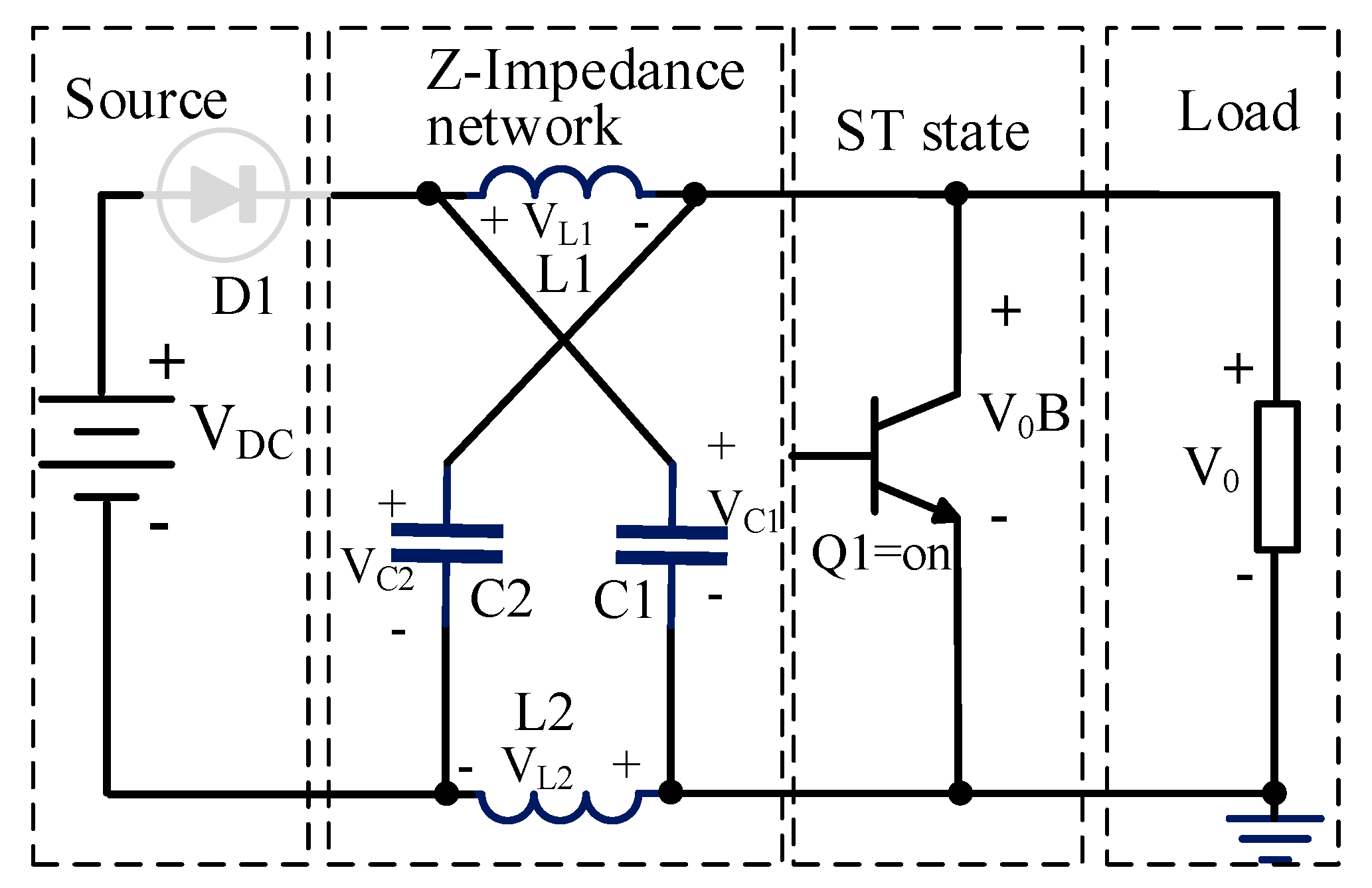
During the ST state shown in Figure 7, switch Q1 is activated (turn-on), short-circuiting the output. Capacitors C1 and C2 are connected in parallel with the inductors and in series with the diode and power supply VDC, polarizing the D1 diode in reverse, so the capacitors charge to the inductors.
In Figure 7, the expressions can be deduced:
V L 1 = V C 1
V L 2 = V C 2
V 0 = V 0 B = 0 .
When performing an energy balance on the inductor, in a steady state, the average voltage of the inductors during a complete period is zero. Here, we are using the expression TS = tST + tNST, where tST is the time in ST state and tNST is the time in NST state.
V L ( t ) S T = 1 T S [ t N S T ( V D C V C ) + t S T V C ]
where
D = t S T T S ; ( 1 D ) = t N S T T S .
Substituting Equation (11) in (10) gives the following expression:
V L ( t ) S T = 1 T S [ T S ( 1 D ) ( V D C V C ) + T S D V C ] = 0
V C V D C = 1 D 1 2 D .
Since VC = VO, the input–output ratio of the Z source converter is determined by:
G = V C V D C = 1 D 1 2 D
where G is the Z-source converter gain as a function of the duty cycle D. Since L1 = L2, the average currents and voltages are identical in both elements. The value of the inductors is linked to the permitted current ripple level ΔiL, and this influences the peak stresses of the power semiconductor devices.
From the following equation:
v ( t ) = L d i d t ,
the following is deduced:
L = v ( t ) d t d t
For the times of the ST and NST states, fs must be the frequency of operation of the converter, di = ΔiL, and v(t) is the voltage applied to the inductor to be analyzed. The value of the inductor is calculated with the following expressions:
L S T = V 0 D f s Δ i L
L N S T = ( V 0 V D C ) ( 1 D ) f s Δ i L
To determine the value of the capacitor, the following equation is used:
i ( t ) = C d v d t
where dv = ΔVC and i(t) is the current applied to the capacitor. The capacitor values for the times of the ST and NST states can be calculated with:
C S T = I i n D f s Δ v C
C N S T = ( I i n ) ( 1 D ) f s Δ v C .

4. Fault Reconfiguration Technique

The reconfiguration technique is based on changing the operating mode of the CMLI from symmetrical to asymmetrical mode. For this purpose, it is necessary to identify the faulted cell to deactivate it and assign the modulation sequence to the remaining fault-free cells.
It is important to emphasize that for the technique proposed here, the nature of the fault does not matter (open circuit or short circuit), because the fundamental principle of the technique is the deactivation of the entire cell. However, it is necessary to point out that this proposal is limited to the fault in a single cell; if there are faults in two or more different cells, this reconfiguration technique cannot be applied.
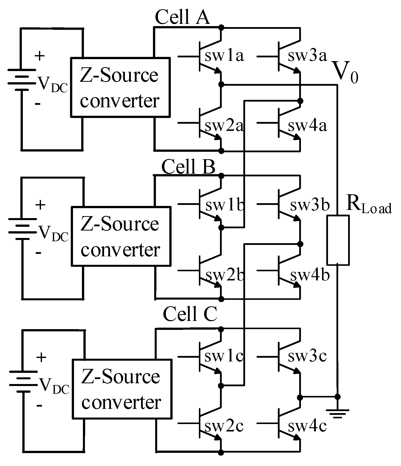
Figure 8 shows the Z-source converter in conjunction with the single-phase seven-level CMLI. This converter is designed to perform a reconfiguration (S-CMLI to A-CMLI) by changing operation in the presence of a fault (fault condition) in one of the three full-bridge cells that conform to the system, changing its output voltage from VDC to double value (2VDC).
Figure 9 shows the flow chart of the methodology used; it is worth mentioning on the one hand that the modifications of the inverter operation from symmetrical to asymmetrical form are made by the cells that compose the multilevel inverter (analytical redundancy), and on the other hand, the variation of the output voltage of the Z source is carried out through the variation of the duty cycle of the gate signal of the semiconductor device that composes the Z source (material redundancy).
Table 1 presents the possible cases of faults analyzed in this paper and the sequence to follow when a fault occurs in a single cell of the CMLI. The goal is to maintain an energy balance; therefore, the duty cycle of the fault-free cells is modified.

5. Experimental Results

Table 2 shows the values of the design parameters of the Z-source inverter, which are divided into fixed and variable values. Variable values change according to the operating condition that can be fault-free condition or fault condition. When a fault occurs in any cell (open circuit fault) in the multilevel converter, the Z source provides twice the output voltage for the multilevel converter modulation to be modified, changing from symmetrical to asymmetrical operating mode.

5.1. Experimental Prototype of the Z-Source Converter

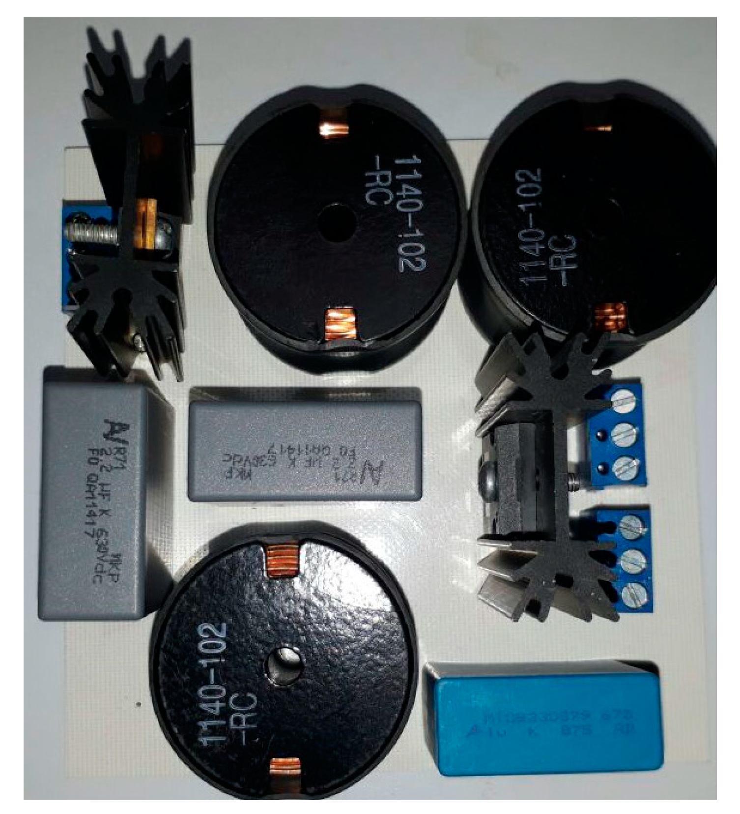
The converter design was implemented in the laboratory to verify its performance. Table 2 lists the electrical parameters of the components used in the implementation. The details are as follows:
  • Diode D1: HFA15TB60 (Ultrafast Diode), rated at 15 A, 600 V (International Rectifier, El Segundo, CA, USA)
  • MOSFET Q1: IRFP350, rated at 10 A, 400 V (Vishay Siliconix, Santa Clara, CA, USA)
  • Inductors L1 and L2: model 1140-102K-RC, 1 mH/5.5 A (Bourns, Jalisco, Mexico)
Figure 10 shows the experimental implementation of the Z-source converter, which was designed from the values in Table 2.

5.2. Z-source Converter Behavior in Transient Mode

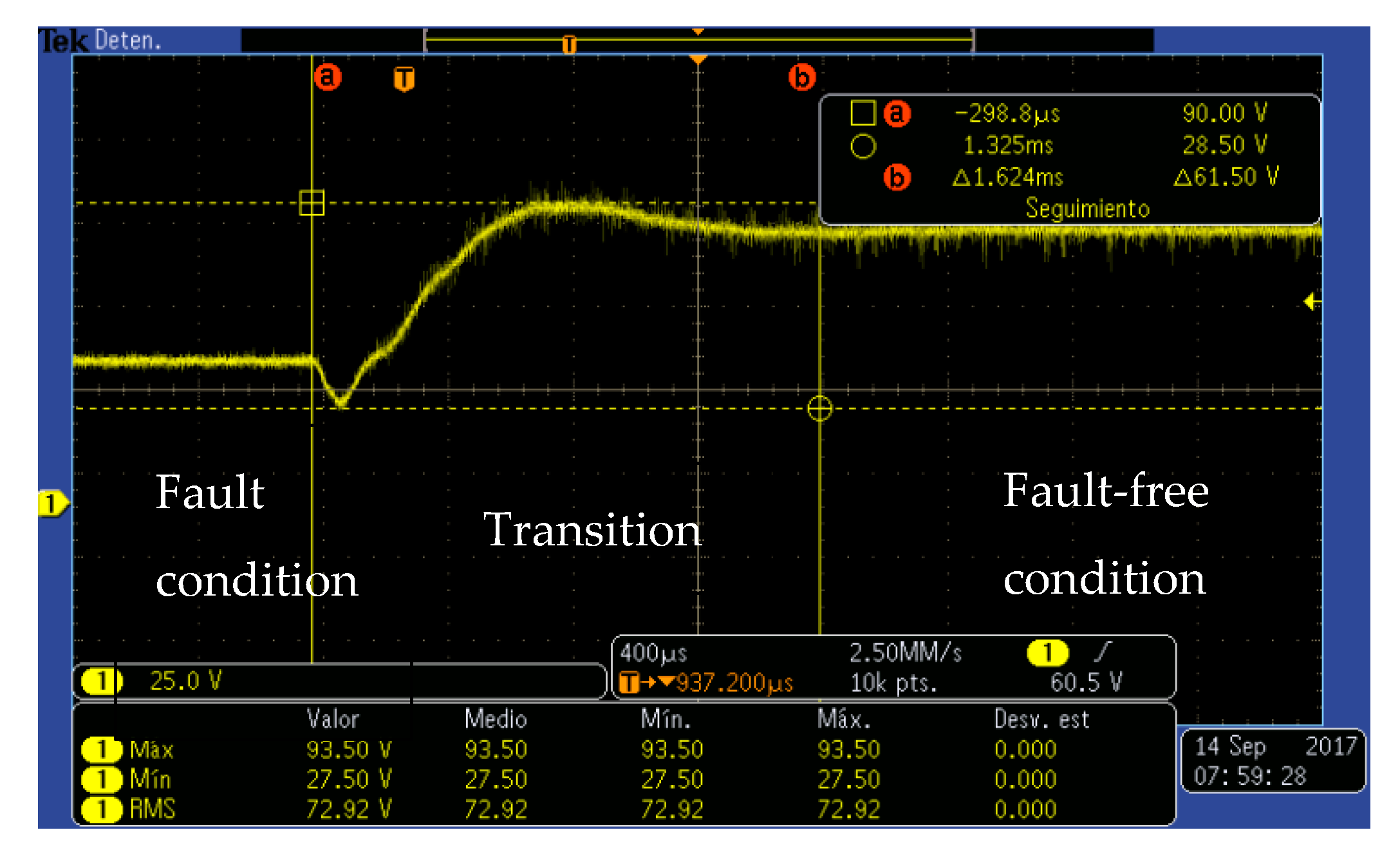
The results obtained experimentally are shown in Figure 11, showing the transition from fault-free condition to fault condition. A transient with a duration of 1.624 ms is presented, with a positive peak voltage of 90 V and a minimum voltage of 28.50 V.

5.3. Multilevel Inverter Behavior in the Fault-Free Condition

The CMLI design was implemented in the laboratory to verify its performance. The electrical parameters of the components used in the implementation are briefly described below:
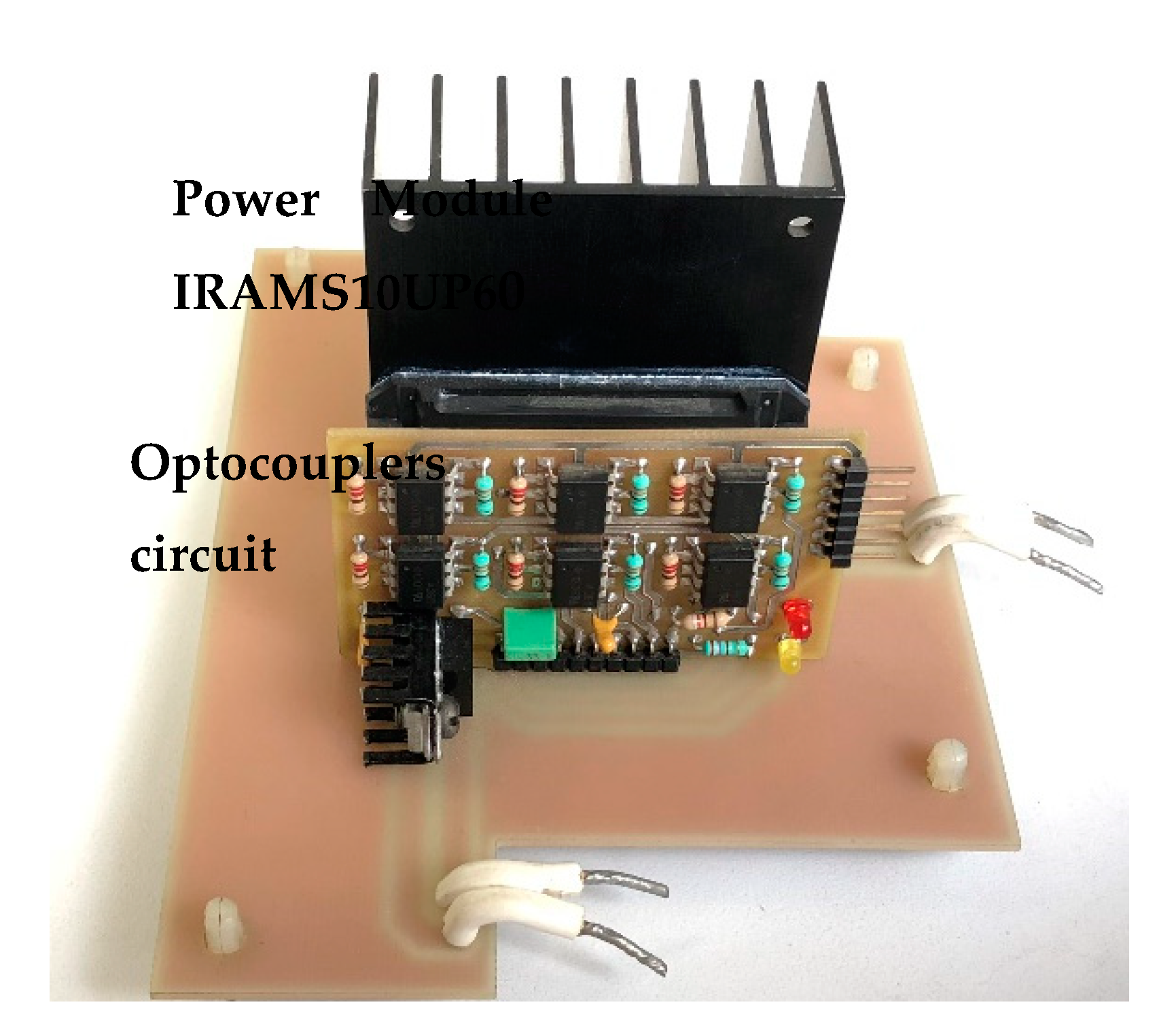
  • Cells A, B, and C: Experimentally built with power modules IRAMS10UP60 (International Rectifier, El Segundo, CA, USA) (These power modules produce a short circuit in the output terminals when any fault occurs in the semiconductor power switches that compose it [21]), rated at 10 A, 600 V (Integrated gate drivers and bootstrap diodes).
  • Optocouplers circuit: A2611 (Fairchild Semiconductor, CA, USA) (The internal shield provides a guaranteed common mode transient immunity specification up to 15,000 V/μs at 1000V).
Figure 12 shows the experimental implementation of a CMLI cell with its drive circuit.
Three 40 V full-bridge cells with three isolated DC power supplies and the Z-source converter were used in the experimental testing stage of the single-phase seven-level CMLI. Figure 13 shows the CMLI operating in fault-free condition, displaying a symmetrical seven-level stepped response.
Figure 14 shows the screenshot of the power quality analyzer, showing the harmonic content of the seven-level symmetrical CMLI output voltage in a fault-free condition. The total harmonic content for the fault-free condition is THD = 5.36% at a frequency of 59.868 Hz, complying with the IEEE 519 standard, which specifies that the maximum total harmonic content permissible is THD = 8%.

5.4. Multilevel Inverter Behavior from the Fault-Free Condition to the Fault Condition (Degraded Response)

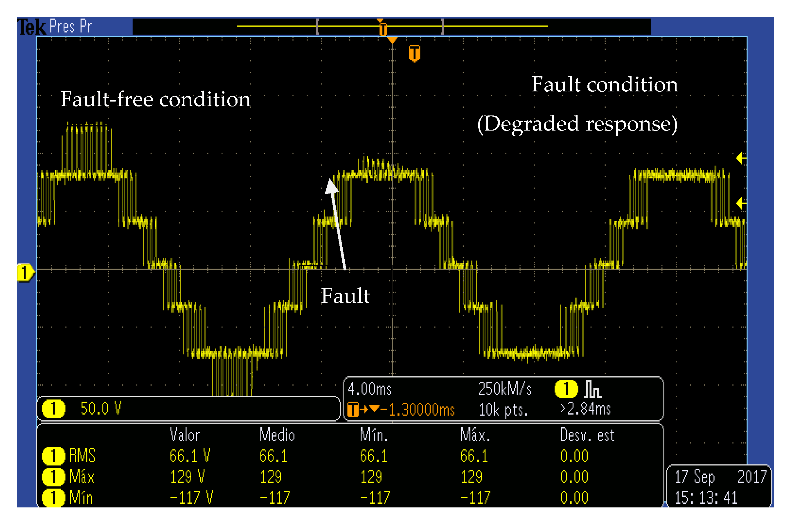
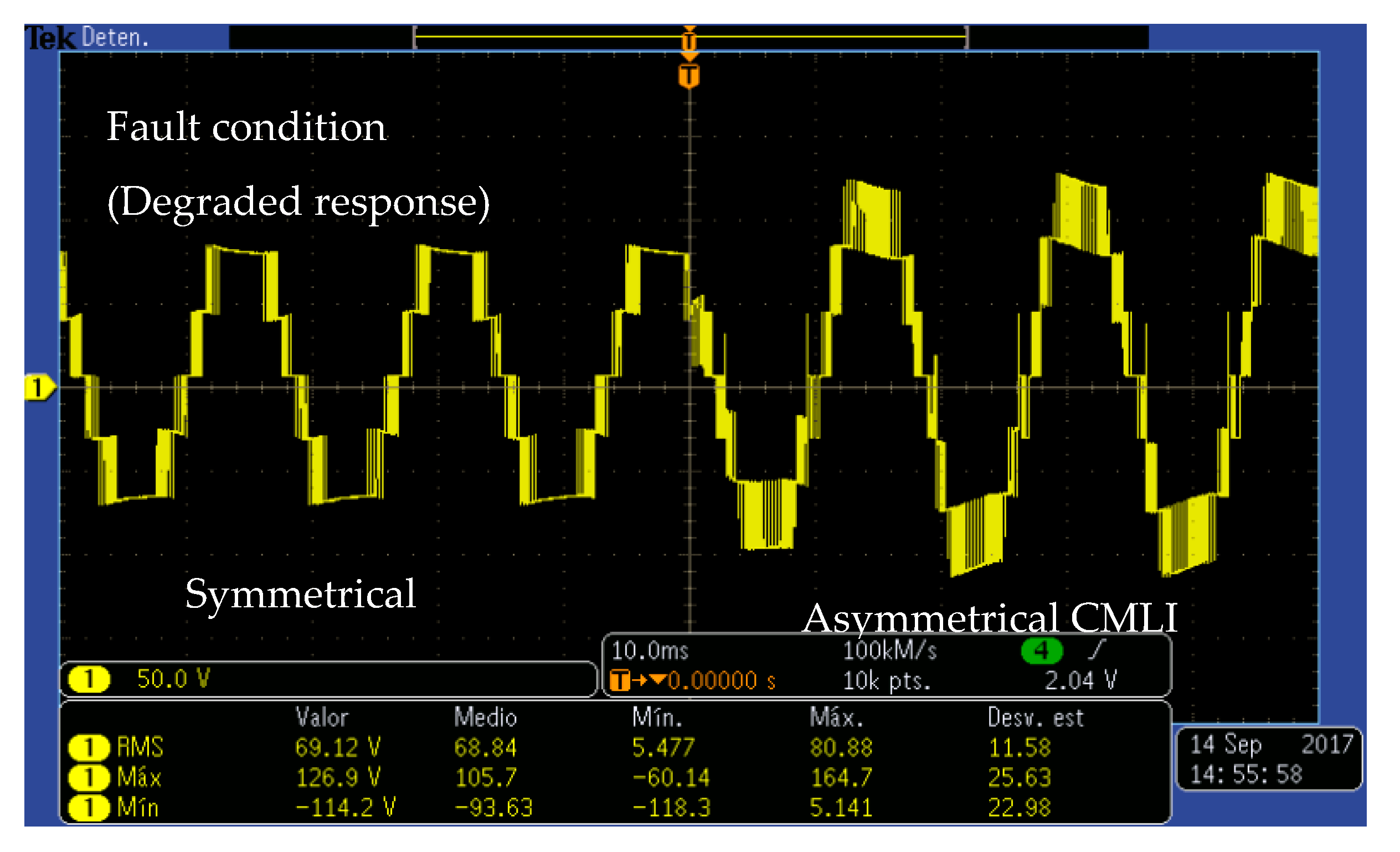
A fault is introduced into the CMLI (in cell “A”), producing a change from a fault-free condition to a fault condition. Therefore, cell “A” is disconnected from the system, resulting in the loss of two voltage levels (one at the top and one at the bottom), presenting a five-level output voltage waveform with a degraded response. Figure 15 shows the five-level voltage waveform obtained.

5.5. Multilevel Inverter Behavior during Fault Condition: Degraded Response Change to Reconfiguration

The Z-source converter (Figure 8) into the CMLI “cell C” produces a change of operation in CMLI from symmetrical to asymmetrical. Therefore, at a time t = 0, the Z-source converter provides a seven-level voltage waveform (as presented in the fault-free condition) of the inverter, as shown in Figure 16.

5.6. Multilevel Inverter Behavior from the Fault-Free Condition to the Fault Condition (Reconfiguration)

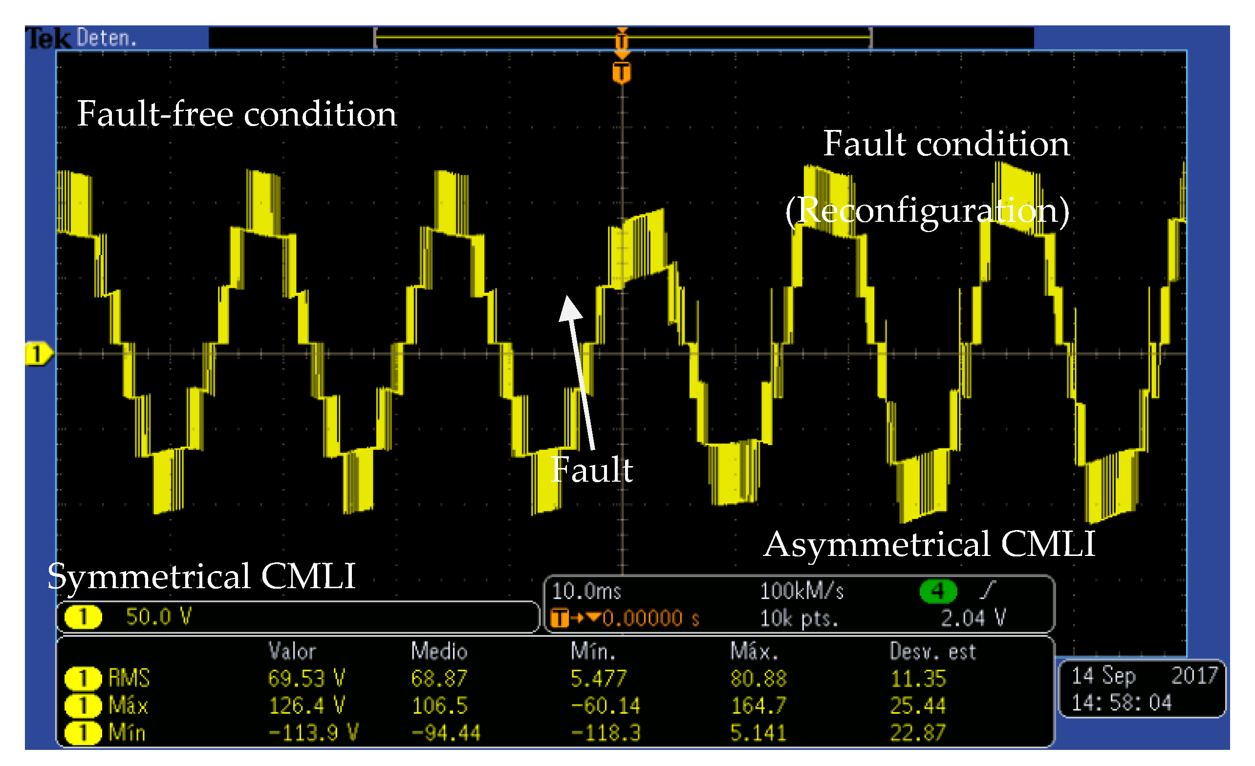
Figure 17 shows the output voltage waveform of the inverter operating in fault-free condition; at instant t = 0, the reconfiguration of the inverter operation is performed, changing from symmetrical to asymmetrical mode. Therefore, a transient state is observed during the change from the fault-free condition to the fault condition.
During the fault condition, the damaged cell of the inverter is automatically short-circuited, and the CMLI is reconfigured (in less than 60 Hz, cycle time = 16.66 ms). The CMLI operated in a degraded regime for a period t < 2 ms.
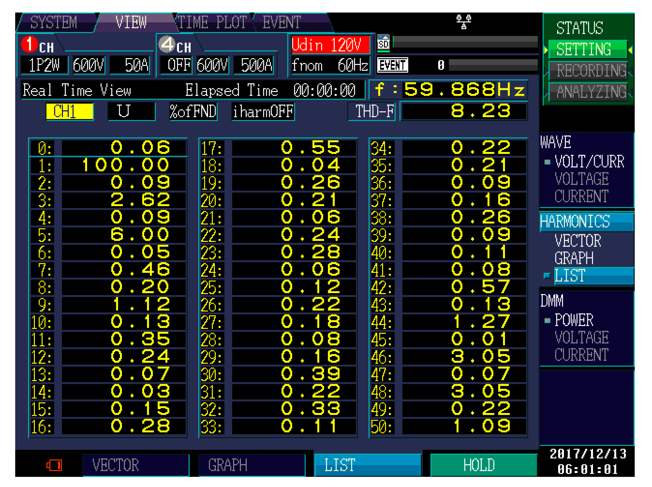
Figure 18 shows the screenshot of the power quality analyzer, showing the harmonic content of the seven-level asymmetrical CMLI output voltage in a reconfigured fault condition, using the Z-source converter, presenting a THD value = 8.23% at a frequency of 59.868 Hz. Therefore, it can be concluded that by reconfiguring the fault-free condition to fault condition, the output voltage signal increases from a THD value of 5.36% to 8.23%.
The speed of response of the Z-source converter allows a reconfiguration in the CMLI in a t < 2 ms. Therefore, if a random failure occurs during the sine wave period, the Z-source converter is capable of restoring the signal, without having phase shift problems, and without negative effects on the output signal cycles.

6. Conclusions

This paper presented the use of the Z-source converter as the main element of fault reconfiguration applied to a seven-level CMLI. The proposed approach combines the modification of the output voltage of the Z-source converter (mathematical redundancy) and the switching sequence of the multilevel inverter (analytical redundancy). Therefore, this combination allows the system to operate symmetrically when the system is in a fault-free condition and asymmetrically when only one fault condition occurs in any of the inverter cells.
The proposed fault tolerance strategy allows the system to operate continuously even when a fault occurs in one of the full-bridge power cells. The strategy allows the CMLI to provide a balanced voltage waveform, even though only two of the three initial power cells operate. This was achieved by performing an operation change on the Z-source converter and using a hybrid modulation technique.
By separating the Z source from the full-bridge inverter stage (single-phase or three-phase) and using it as a DC-DC converter, the Z-source converter can be operated at high frequency (100 kHz). Therefore, the switching frequency is no longer limited by the IGBTs used in the CMLI, and the dynamic response of the inverter is around 2 ms. This allows the output voltage value to be doubled when a change in operation occurs in the presence of a fault (fault condition). In contrast, the applications where the Z source is connected directly to the inverter exhibit a dynamic response with a duration of about 250 ms.

Author Contributions

Conceptualization, J.A.-A., I.V.-L., S.E.D.L.-A., and M.P.-S.; data curation, R.E.L.-P., E.F.-R. and J.G.-M.; formal analysis, J.A.-A., I.V.-L., S.E.D.L.-A. and M.P.-S.; funding acquisition, M.M.-R., R.E.L.-P., E.F.-R., Y.R.-S., L.M.C.-S. and E.M.A.-C.; investigation, J.A.-A., I.V.-L. and S.E.D.L.-A.; methodology, J.A.-A., S.E.D.L.-A. and I.V.-L.; project administration, J.A.-A. and S.E.D.L.-A.; resources, R.E.L.-P., E.F.-R., and J.G.-M.; software, Y.R.-S., E.M.A.-C., L.M.C.-S., M.M.-R., and I.V.-L.; supervision, J.A.-A. and S.E.D.L.-A.; validation, J.A.-A., I.V.-L. and S.E.D.L.-A.; visualization, J.G.-M., R.E.L.-P., E.F.-R. and M.P.-S.; writing—original draft, J.A.-A., S.E.D.L.-A. and I.V.-L.; writing—review and editing, J.A.-A., S.E.D.L.-A., M.P.-S. and R.E.L.-P. All authors have read and agreed to the published version of the manuscript.

Funding

This research received no external funding.

Conflicts of Interest

The authors declare no conflict of interest.

References

  1. Aldaco, S.E.D.L.; Calleja, H.; Alquicira, J.A. Reliability and Mission Profiles of Photovoltaic Systems: A FIDES Approach. IEEE Trans. Power Electron. 2015, 30, 2578–2586. [Google Scholar] [CrossRef]
  2. Aldaco, S.E.D.L.; Calleja, H.; Alquicira, J.A. Metaheuristic Optimization Methods Applied to Power Converters: A Review. IEEE Trans. Power Electron. 2015, 30, 6791–6803. [Google Scholar] [CrossRef]
  3. Kumar, P.V.; Fernandes, B.G. A Fault-Tolerant Single-Phase Grid-Connected Inverter Topology with Enhanced Reliability for Solar PV Applications. IEEE J. Emerg. Sel. Top Power Electron. 2017, 5, 1254–1262. [Google Scholar] [CrossRef]
  4. Rodríguez-Blanco, M.; Vzquez-Prez, A.; Hernndez-Gonzlez, L.; Golikov, V.; Aguayo-Alquicira, J.; May-Alarcn, M. Fault Detection for IGBT Using Adaptive Thresholds During the Turn-on Transient. IEEE Trans. Ind. Electron. 2015, 62, 1975–1983. [Google Scholar] [CrossRef]
  5. JALHOTRA, M.; Kumar, L.; GAUTAM, S.; Gupta, S. Development of fault tolerant multilevel inverter topology. IET Power Electron. 2018, 11, 1416–1424. [Google Scholar] [CrossRef]
  6. Kumar, M.S.; Borghate, V.B.; Karasani, R.R.; Sabyasachi, S.; Suryawanshi, H.M. A fault-tolerant modular multilevel inverter topology. Int. J. Circuit Theory Appl. 2018, 46, 1028–1043. [Google Scholar] [CrossRef]
  7. Chatzakis, J.; Antonidakis, E. A novel N+k fault-tolerant hot-swap DC/AC inverter design. In Proceedings of the 2008 IEEE Power Electronics Specialists Conference, Rhodes, Greece, 15–19 June 2008; pp. 3291–3294. [Google Scholar]
  8. Rodriguez-Blanco, M.A.; Claudio-Sanchez, A.; Theilliol, D.; Vela-Valdes, L.G.; Sibaja-Teran, P.; Hernandez-Gonzalez, L.; Aguayo-Alquicira, J. A Failure-Detection Strategy for IGBT Based on Gate-Voltage Behavior Applied to a Motor Drive System. IEEE Trans. Ind. Electron. 2011, 58, 1625–1633. [Google Scholar] [CrossRef]
  9. Kwak, Y.-G.; Heo, D.-H.; Kim, S.-P.; Song, S.-G.; Park, S.-J.; Kang, F.-S. Reliability and Economic Efficiency Analysis of 4-Leg Inverter Compared with 3-Leg Inverters. Electronics 2021, 10, 87. [Google Scholar] [CrossRef]
  10. Dixon, J.; Barriuso, P.; Ortuzar, M.; Moran, L.; Pontt, J.; Rodriguez, J. Fault Tolerant Reconfiguration System for Asymmetric Multilevel Converters Using Bi-Directional Power Switches. In Proceedings of the IECON 2007-33rd Annual Conference of the IEEE Industrial Electronics Society, Taipei, Taiwan, 5–8 November 2007; pp. 2124–2129. [Google Scholar]
  11. Abbasi, S.; Ghadimi, A.A.; Abolmasoumi, A.H.; Miveh, M.R.; Jurado, F. Enhanced Control Scheme for a Three-Phase Grid-Connected PV Inverter under Unbalanced Fault Conditions. Electronics 2020, 9, 1247. [Google Scholar] [CrossRef]
  12. Ma, M.; Hu, L.; Chen, A.; He, X. Reconfiguration of Carrier-Based Modulation Strategy for Fault Tolerant Multilevel Inverters. IEEE Trans. Power Electr. 2007, 22, 2050–2060. [Google Scholar] [CrossRef]
  13. Kim, S.-M.; Lee, J.-S.; Lee, K.-B. A Novel Modulation Strategy Based on Level-Shifted PWM for Fault Tolerant Control of Cascaded Multilevel Inverters. Trans. Korean Inst. Electr. Eng. 2015, 64, 718–725. [Google Scholar] [CrossRef] [Green Version]
  14. Turpin, C.; Baudesson, P.; Richardeau, F.; Forest, F.; Meynard, T. Fault management of multicell converters. IEEE Trans. Ind. Electron. 2002, 49, 988–997. [Google Scholar] [CrossRef]
  15. Vargas, R.A.; Figueroa, A.; Aldaco, S.E.D.L.-; Aguayo, J.; Hernández, L.; Rodriguez, M.A. Analysis of Minimum Modulation for the 9-Level Multilevel Inverter in Asymmetric Structure. IEEE Lat. Am. Trans. 2015, 13, 2851–2858. [Google Scholar] [CrossRef]
  16. Malinowski, M.; Gopakumar, K.; Rodriguez, J.; Perez, M.A. A Survey on Cascaded Multilevel Inverters. IEEE Trans. Ind. Electron. 2009, 57, 2197–2206. [Google Scholar] [CrossRef]
  17. Ye, M.; Ren, W.; Wei, Q.; Song, G.; Miao, Z. Research on Modified Hybrid Frequency Modulation Technology of Type-III Asymmetric CHB Multilevel Inverters. Electronics 2020, 9, 263. [Google Scholar] [CrossRef] [Green Version]
  18. Peng, F.Z. Z-source inverter. IEEE Trans. Ind. Appl. 2003, 39, 504–510. [Google Scholar] [CrossRef]
  19. Grgić, I.; Vukadinović, D.; Bašić, M.; Bubalo, M. Calculation of Semiconductor Power Losses of a Three-Phase Quasi-Z-Source Inverter. Electronics 2020, 9, 1642. [Google Scholar] [CrossRef]
  20. Chitra, K.; Jeevanandham, A. Design and implementation of maximum constant boost switched inductor z-source inverter for three-phase on-line uninterrupted power supply. COMPEL Int. J. Comput. Math. Electr. Electron. Eng. 2015, 34, 1101–1121. [Google Scholar] [CrossRef]
  21. Datasheet IRAMS10UP60. Available online: https://www.alldatasheet.com/view_datasheet.jsp?Searchword=IRAMS10UP60 (accessed on 1 February 2021).
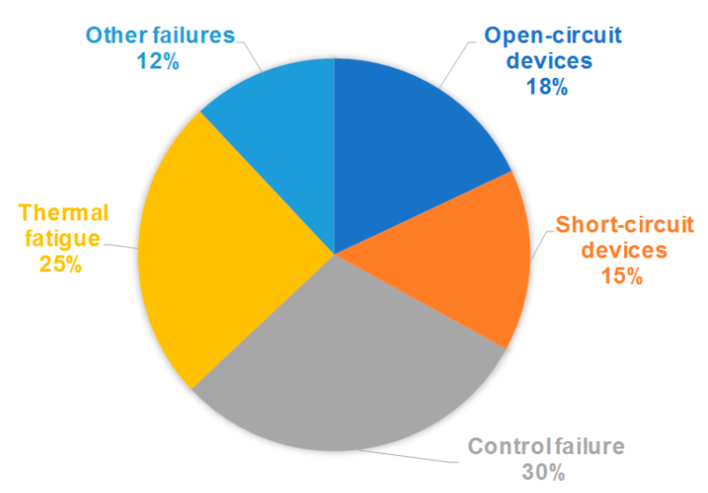
Figure 1. Pie diagram of failure distribution in power semiconductor devices.
Electronics 10 00574 g001
Figure 2. (a) Diagram of symmetrical cascaded multilevel inverter with a seven-level, single-phase structure. (b) Output voltage waveform.
Electronics 10 00574 g002
Figure 3. (a) Diagram of asymmetrical cascaded multilevel inverter with a seven-level, single-phase structure. (b) Output voltage waveform.
Electronics 10 00574 g003
Figure 4. Electrical diagram of a three-phase full-bridge Z-source inverter.
Electronics 10 00574 g004
Figure 5. Electrical diagram of Z-source converter.
Electronics 10 00574 g005
Figure 6. Electrical diagram of Z-source converter in the Non-Shoot-Through (NST) state.
Electronics 10 00574 g006
Figure 7. Electrical diagram of Z-source converter in the Shoot-Through (ST) state.
Electronics 10 00574 g007
Figure 8. Combination of cascade multilevel inverters (CMLI) with the Z-source converter, used for reconfiguration purposes.
Electronics 10 00574 g008
Figure 9. Flowchart of the methodology used.
Electronics 10 00574 g009
Figure 10. Electrical components of the experimental implementation of the Z-source converter.
Electronics 10 00574 g010
Figure 11. Oscillogram of the transient state of Z-source converter, during its operation change.
Electronics 10 00574 g011
Figure 12. Electrical components of the experimental implementation of a CMLI cell with its drive circuit.
Electronics 10 00574 g012
Figure 13. Oscillogram of the seven-level cascade multilevel inverter output voltage waveform in fault-free condition.
Electronics 10 00574 g013
Figure 14. List of Total Harmonic Distortion (THD) value of the CMLI in the ideal case (power supplies of equal value).
Electronics 10 00574 g014
Figure 15. Oscillogram of the output voltage waveform behavior during the change from the fault-free condition to the fault condition (degraded response).
Electronics 10 00574 g015
Figure 16. Oscillogram of the output voltage waveform behavior during fault condition: degraded response change to reconfiguration.
Electronics 10 00574 g016
Figure 17. Oscillogram of the output voltage waveform behavior during the change from the fault-free condition to the fault condition (Reconfiguration).
Electronics 10 00574 g017
Figure 18. List of THD value of the seven-level asymmetrical CMLI in a reconfigured fault condition.
Electronics 10 00574 g018
Table 1. Possible cases of CMLI with fault tolerance.
ConditionCell ACell BCell C
Fault-freeCMLI in symmetric mode.
Z-Source in fault-free condition.
CMLI in symmetric mode.
Z-Source in fault-free condition.
CMLI in symmetric mode.
Z-Source in fault-free condition.
Fault in Cell ACMLI in short-circuit mode.
Z-Source in OFF mode.
CMLI in asymmetric mode.
Z-Source in fault-free condition.
CMLI in asymmetric mode.
Z-Source in fault mode.
Fault in Cell BCMLI in asymmetric mode.
Z-Source in fault mode.
CMLI in short-circuit mode.
Z-Source in OFF mode.
CMLI in asymmetric mode.
Z-Source in fault-free condition.
Fault in Cell CCMLI in asymmetric mode.
Z-Source in fault-free condition.
CMLI in asymmetric mode.
Z-Source in fault mode.
CMLI in short-circuit mode.
Z-Source in OFF mode.
Table 2. Z-source converter design parameters.
Figure ParameterValue
VDC 38   V
C1 & C2 2.2   µ F
L1 & L2 1   mH
RLOAD 64   Ω
LX 1   mH
CX 1   µ F
fs 100   kHz
Variable ParameterFault-Free Condition (Nominal)Fault Condition
V0 40   V 80   V
P0 25   W 100   W
D 0.048 0.344
ΔiL 0.02   A 0.25   A
ΔVC0.15 V 4   V
Publisher’s Note: MDPI stays neutral with regard to jurisdictional claims in published maps and institutional affiliations.