Abstract
Compensation is crucial in the inductive power transfer system to achieve load-independent constant voltage or constant current output, near-zero reactive power, higher design freedom, and zero-voltage switching of the driver circuit. This article proposes a simple, comprehensive, and innovative graphic design methodology for compensation topology to realize load-independent output at zero-phase-angle frequencies. Four types of graphical models of the loosely coupled transformer that utilize the ideal transformer and gyrator are presented. The combination of four types of models with the source-side/load-side conversion model can realize the load-independent output from the source to load. Instead of previous design methods of solving the equations derived from the circuits, the load-independent frequency, zero-phase angle (ZPA) conditions, and source-to-load voltage/current gain of the compensation topology can be intuitively obtained using the circuit model given in this paper. In addition, not limited to only research of the existing compensation topology, based on the design methodology in this paper, 12 novel compensation topologies that are free from the constraints of transformer parameters and independent of load variations are stated and verified by simulations. In addition, a novel prototype of primary-series inductor–capacitance–capacitance (S/LCC) topology is constructed to demonstrate the proposed design approach. The simulation and experimental results are consistent with the theory, indicating the correctness of the design method.
1. Introduction
Compared to traditional plug-in systems, inductive wireless energy transmission systems have advantages such as flexibility, convenience, electrical isolation, and strong environmental adaptability [1]. It has been employed in many applications. For example, in the field of electric vehicles, the inductive power transfer (IPT) method has a greater advantage for the electric vehicle (EV) battery charger due to its convenience and safety as compared to the plugged-in charger [2]. In the area of implantable medical devices, compared to batteries, IPT can theoretically achieve an unlimited lifetime through wireless power transfer, without the need for surgery to replace the battery, greatly reducing the patient’s pain [3]. In the field of consumer electronics, inductively coupled chargers are becoming more and more popular in wireless charging of mobile phones, laptops, and other handheld devices as proposed in [4].
Figure 1 illustrates the schematic diagram of an IPT system. At the primary side, the IPT system is powered by a DC source UDC (IDC), and the inverter produces a constant AC voltage or current. At the secondary side, a rectifier is applied to generate a DC voltage to the load ZL. As shown in Figure 1, in order to transfer power within a certain distance in the IPT system, a loosely coupled transformer (LCT) that involves the primary coil and the secondary coil must be used. Due to the existence of the air gap between the coils, when the distance of the coils increases, the coupling coefficient between the coils becomes smaller while leakage inductance becomes bigger. Uncoupled magnetic flux generates significant reactive power, which increases the ratings of the drive circuit and reduces the power transfer capability [5]. Therefore, compensation circuits are generally required to achieve or improve the following characteristics:
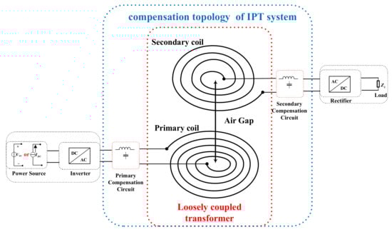
Figure 1.
Schematic diagram of a typical inductive power transfer (IPT) system.
- Implementing the zero-phase angle (ZPA) feature. In order to achieve near-zero reactive power and transfer more power to the load, it is desirable for the IPT system to operate at the zero-phase-angle frequency [6]. At this frequency, the equivalent impedance seen by the source is a pure resistance, minimizing the volt-ampere (VA) ratings of the power supply and maximizing the transfer capability.
- Facilitating zero-voltage switching (ZVS) and improving system efficiency. Hard switching refers to the phenomenon that the current and voltage on the power switch overlap in a large area during the turn-on process of the power switch. This is the main contributor to energy loss. Especially when the switching frequency is high, the conversion rate of the power supply in the hard-switching state decreases, the switching loss and the stress it bears also increases exponentially, which greatly reduces the switching efficiency. The zero-voltage switching is to turn MOS on when the voltage crosses zero, which requires the circuit to be slightly inductive when the current crosses zero, thus causing resonant-tank current to lag the voltage. In this way, the overlap area of voltage and current during turn-on is reduced, thereby reducing loss and obtaining higher efficiency. It is worth noting that based on the realization of near-zero reactive power, only a small adjustment of the compensation parameters can make the circuit appear slightly inductive to facilitate ZVS [5]. Therefore, it is critical to design the parameters of the compensation circuit properly to realize the characteristics of ZPA.
- Load-independent constant-voltage (CV) or constant-current (CC) output. In wireless power transmission systems, load-independent CV or CC output is necessary in many cases. In recent years, lithium-ion batteries are increasingly used in EVs [7,8]. To ensure the safety of the lithium-ion battery and the effectiveness of the charging system, proper charging strategies are crucial [9]. Constant-current–constant-voltage charging is often adopted due to efficiency and safety. The typical charging process of an EV lithium-ion battery is shown in Figure 2 [10]. It can be seen from Figure 2 that the charging process is divided into two stages. The first stage is a constant current process, with the charging current basically unchanged and the battery voltage rising rapidly. The second stage is a constant-voltage process. When the battery voltage reaches the specified level, the charger enters the CV charging process, where the battery voltage remains basically unchanged and the charging current gradually decreases until it approaches zero. In addition, in order to ensure the safe operation of the implantable devices, the output voltage must remain basically unchanged within a large range of load changes [11]. Designing the compensation topology meticulously can be a better alternative compared to utilizing a backend DC–DC converter or frequency control, which makes the control circuits simplified to obtain better system stability and reduce energy loss to improve system efficiency.
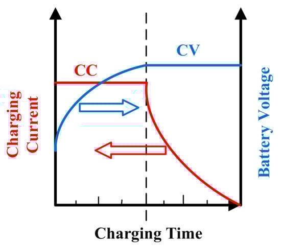 Figure 2. Constant-current–constant-voltage charging of a lithium-ion battery cell.
 - Freeing from LCT parameters to get higher design freedom. Low design freedom means that the input-to-output transfer function is dependent on LCT parameters, which implies the fact that once the input voltage or current is predetermined, the output voltage or current does not change unless a new LCT with different parameters is used [12]. However, the redesign of the LCT is time-consuming and complex. In consequence, designing the compensation topology with the input-to-output transfer function independent of LCT parameters is of great importance.
- Less use of compensation components. The authors of [13] proposed a compensation topology, named double-side LCC compensation topology, which poses all the above mentioned characteristics including ZPA, ZVS, load-independent output current, and source-to-load transfer function independent of LCT parameters. However, it has six compensation elements, including one inductor and two capacitors at both the primary and secondary sides, which results in higher cost, more space, and a lower power density. Therefore, the use of fewer compensation elements while satisfying other characteristics mentioned above is also significant.
Some researchers have analyzed and designed how to realize the required characteristics for the compensation topology of an IPT system. Based on the traditional mutual inductance model of the LCT, the literature [14] adopted the method of the separation of parameters to obtain the conditions of CV or CC. However, this approach of solving the equations derived from circuits can be tedious and time consuming. Moreover, the research has not made a comprehensive and systematic analysis of the ZPA characteristics of topology. Reference [15] shows that by correctly combining resonant blocks with CC/CV output functions, compensation structures can achieve a constant output and a minimum input VA rating simultaneously. However, for some topologies, the method of separating parameters is still used to obtain the compensation parameters of CC or CV, and the given model cannot intuitively reach the conditions of realizing ZPA. The literature [16] proposes a general modeling method based on the basic LC network, T-network, and π-network for realizing load-independent current and voltage output for compensation networks. However, this method is not straightforward and does not analyze the ZPA characteristic. In reference [17], the compensation topologies are modeled as basic L-Section matching networks and the regularization mathematical expressions of load-independent current or voltage and the realization conditions of ZPA are given. However, it is not straightforward to solve the mathematical model of the circuit to obtain the conditions for constant output and pure input resistance. A graphical approach method [18] based on gyrator is proposed to visually and systematically analyze the CC/CV output with ZPA operation of compensation topologies. However, CC/CV output and ZPA conditions cannot be obtained simultaneously by intuitive analysis.
Therefore, there are three common deficiencies in the above researches.
- The modeling method is not intuitive. The compensation circuits are analyzed in the above literature mainly by mathematical methods. By solving the equation derived from the circuit or matrix manipulation, the characteristics of the compensation circuit are obtained, although the equation approach may be universal and unified. However, it is usually tedious and time consuming;
- In addition, all the above researches use new models or adopt a new perspective to analyze the existing compensation circuits, some of the literature focuses on how to design a new compensation topology with higher design freedom and fewer compensating components;
- The polarity of induced voltage is ignored. Under different resonant conditions, the voltage waveform of the secondary coil and that of the primary coil may be in-phase or antiphase. This causes the equivalent model to have two symbols and frequency bifurcation phenomena.
As a supplement and improvement of previous design methods, a graphical and simple design methodology is proposed in this paper. The ideal transformer and ideal gyrator are adopted to establish four types of models for LCT: CV input to CV output, CV input to CC output, CC input to CV output, and CC input to CC output. Two models of voltage-current conversion at the source and load side are also constructed. The combination of four types of LCT models with the source-side/load-side conversion models can realize the load-independent CV or CC output from voltage/current source to load. Based on the above design methodology, 12 novel compensation topologies fed by a voltage source are stated. They all provide the characteristics of ZPA, easy achievement of ZVS, load-independent CV or CC output, and LCT-unconstrained transfer function. The conditions of these characteristics can be obtained only by simply observing the equivalent model given by the design method in this paper, giving a new perspective being free from the constraints of complex equations. Moreover, compared to compensation topologies with less than three compensation elements, including S/S compensation topology, S/PS compensation topology, S/P compensation topology, and S/SP compensation topology, our topologies have source-to-load transfer functions independent of LCT parameters, which makes it possible to change the output power without replacing the LCT. Compared to double-sided LCC compensation topology, they all have fewer compensation components, which means lower cost, less space, and higher power density. In order to further verify theoretical analysis, a new prototype of S/LCC topology is constructed. The experimental results match well with the theory, validating the rightness of the newly proposed design method.
The remainder of this paper is structured as follows: Section 2 gives the overall design block diagram of the IPT system to achieve load-independent voltage and current output. Section 3 discusses four types of models of LCT that utilize the ideal transformer and ideal gyrator for realizing conversion from CV/CC input to CV/CC output. Section 4 presents two models of voltage and current conversion at the source and load side. Section 5 analyzes the detailed design methodology for designing compensation circuits to realize load-independent CV or CC output at ZPA frequencies. Section 6 demonstrates simulation and experimental results. Section 7 compares the design methods of this paper with those of other previous works. Finally, the entire work is concluded in Section 8.
2. The Proposed Design Diagram
Figure 3 shows the design diagram for the compensation circuit with load-independent CV or CC output in IPT systems. At the primary side, the DC source and the inverter can be equivalent to the AC voltage/current source with the fundamental harmonic approximation. At the secondary side, the rectifier and load ZL can be represented by an equivalent resistance RL with the value of , as shown in Figure 2.
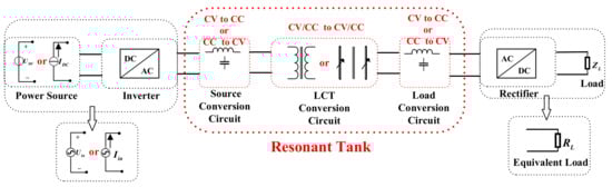
Figure 3.
Design diagram for compensation circuit with load-independent constant-voltage (CV) or constant-current (CC) output in IPT systems.
In order to achieve load-independent constant-voltage or constant-current output from the AC source to the equivalent resistance, the design of compensation circuits is divided into three sections as displayed in Figure 3: source-side conversion circuits, load-side conversion circuits, and LCT conversion circuits. Both source-side and load-side circuits are designed to convert voltage to current or convert current to voltage. The LCT compensation models can realize the conversion of voltage and current in four forms: CV input to CV output, CV input to CC output, CC input to CV output, and CC input to CC output. It is clear to see that by properly combining four types of the LCT models with the source-side and load-side conversion circuits, we can realize the load-independent CV or CC output from voltage/current source to load.
3. Modeling of Constant Voltage/Current to Constant Voltage/Current for Loosely-Coupled Transformers
The loosely coupled transformer can be simplified by the mutual inductance model in the circuit [19], as shown in Figure 4. L1 and L2 are the self-inductance of the transmitting coil and the receiving coil, respectively. M is the mutual inductance, and always holds. is the coupling coefficient between the coils. The magnitude of the induced voltage generated by the primary coil of the secondary circuit is , similarly the magnitude of the induced voltage generated by the secondary coil of the primary circuit is . I1 and I2 are the currents flowing through the primary and secondary coils. represents the operating angular frequency of the LCT system. ““ represents the polarity of the induced voltage, which depends on the relative polarity of the mutually coupled coils.
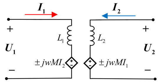
Figure 4.
Mutual inductance equivalent model of loosely coupled transformer (LCT).
3.1. The Model of Constant Voltage to Constant Voltage
U1 and U2 are the voltage across the primary and secondary coils, respectively. After introducing a common factor , we can transform (1) to (2).
It can be proven that the LCT can be modeled as Figure 5. The two circuits in Figure 5 are equivalent based on the impedance conversion rule of an ideal transformer. Applying Kirchhoff’s law on the left and right circuit in Figure 5, respectively, we can get (2a) and (2b), which demonstrate equivalence between the LCT with the circuits of Figure 5. As shown in Figure 5, A is the voltage transfer ratio of the ideal transformer. Part A is the series inductor of the primary circuit, and its value is . Part B is the series inductor for the secondary circuit, and its value is . Part C is the parallel inductor with a value of at the primary side or the parallel inductor with a value of at the secondary side. If part A and part B equal 0 at the same time, then and are and , respectively. Therefore, the scale factor of and becomes 1/A, which means that the output from constant voltage to constant voltage is realized. There are three cases in which part A and part B can both be equal to 0, each with different value of A leading to three types of constant-voltage to constant-voltage conversion models of the LCT, which are shown in Table 1 and Figure 6, Figure 7 and Figure 8.
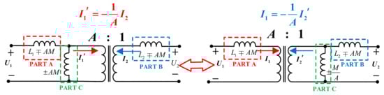
Figure 5.
Equivalent circuit of the LCT from constant voltage to constant voltage.

Table 1.
Modeling of constant voltage to constant voltage for loosely coupled transformers.
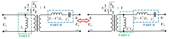
Figure 6.
The equivalent model of the I_CV_CV circuit.
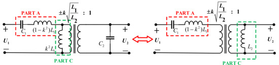
Figure 7.
The equivalent model of the II_CV_CV circuit.
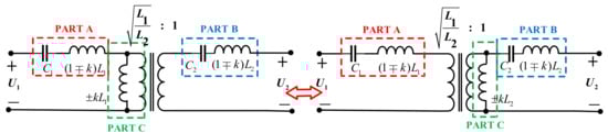
Figure 8.
The equivalent model of the III_CV_CV circuit.
3.2. The Model of Constant Voltage to Constant Current
In accordance with (1), the Z matrix of the LCT is
If we convert Z matrix to H matrix, we can have H matrix of the LCT as
Similarly, if we introduce a common factor , then we can transform (4) into
In order to obtain the constant voltage to constant-current conversion model of the LCT, we first introduce the gyrator theory. The gyrator is a two-port network first proposed by Tellegen in 1948 [20]. As opposed to the ideal transformer whose voltage at one port is proportional to the voltage at the other, an ideal gyrator can convert the voltage at one port to the current at the other in a fixed scaling factor.
The voltage-current relationship of the ideal gyrator as shown in Figure 9 is
where and are the phasors of the primary-port current and voltage of the gyrator. and represent the phasors form of the secondary-port current and voltage. A is the transfer ratio of an ideal gyrator. The authors of (6) imply the fact that if the primary voltage is fixed, the gyrator makes the secondary current a fixed ratio to the primary voltage. Therefore, the gyrator can be used to construct the LCT model for achieving the conversion of constant voltage to a constant current.
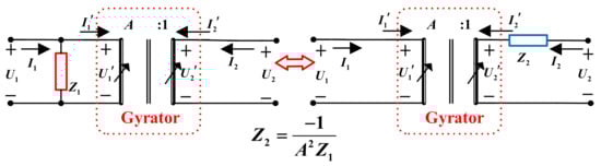
Figure 9.
Impedance inversion of a gyrator.
It can be proven that parallel-connected impedance at the primary port can be converted to series-connected impedance at the second port while not affecting voltage–current relationships (, , , and ) between input and output. and are the input voltage and current of the external port. and represent the output voltage and current of the external port.
By applying Kirchhoff’s law to the circuit on the left of Figure 9, the voltage–current relationship of the port can be obtained as
Similarly, the same voltage–current relationship can be deduced from the circuit on the right of Figure 9, indicating that the two circuits in Figure 9 are completely equivalent.
Therefore, the impedance inversion relationship of the ideal gyrator is
Based on the current–voltage conversion and impedance conversion relationships of the ideal gyrator, we can prove that the loosely coupled transformer can be converted into the model in Figure 10. The two circuits in Figure 10 are equivalent due to (8). As shown in Figure 10, Part A is a series inductor for the primary circuit, and its value is . Part B is a parallel inductor for the secondary circuit, and its value is . Part C is a parallel inductor with a value of at the primary side or a series inductor with a value of at the secondary side.
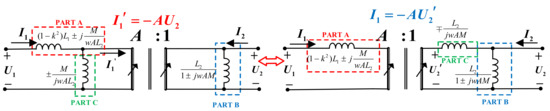
Figure 10.
Equivalent circuit of the LCT from constant voltage to constant current.
It is clear to see that (5a) and (9) are equivalent, and the same is true for (5b) and (10), which proves that the LCT can be modeled after the circuit of Figure 9. Therefore, if part A and part B equal 0 at the same time, then and are and , respectively, and the scale factor of and becomes −A. A is the transfer ratio of an ideal gyrator. Therefore, by adjusting the transfer ratio A and adding the compensation capacitor, the values of Part A and Part B can be 0 at the same time to make the output current I2 and the input voltage U1 become a fixed ratio −A, which means that the output from constant voltage to constant current is realized. There are three ways in which A and B can both be equal to 0, which are presented in Table 2 and Figure 11, Figure 12 and Figure 13.
Table 2.
Modeling of constant voltage to constant current for loosely coupled transformers.
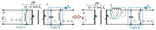
Figure 11.
The equivalent model of the I_CV_CC circuit.
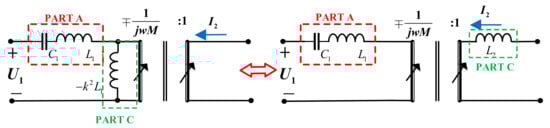
Figure 12.
The equivalent model of the II_CV_CC circuit.
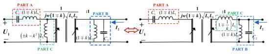
Figure 13.
The equivalent model of the III_CV_CC circuit.
3.3. The Model of Constant Current to Constant Current Model
To achieve constant current to constant current output, the Z parameter matrix of the system is converted into a Y parameter matrix as follows:
If we introduce the common factor , we transform (11) into
Considering that the primary-port current and secondary-port current of the ideal transformer are a fixed ratio, we can model the LCT as a circuit based on the transformer. As with the analysis in Section 3.1 and Section 3.2, the analysis process and modeling results are shown in Figure 14, Figure 15 and Figure 16.
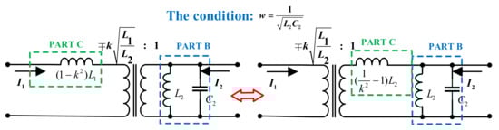
Figure 14.
The equivalent model of the I_CC_CC circuit.
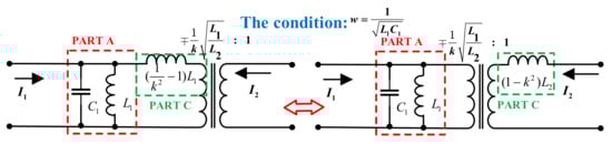
Figure 15.
The equivalent model of the II_CC_CC circuit.
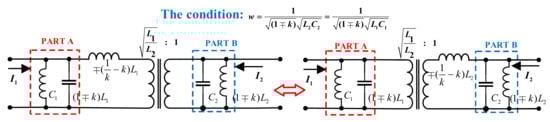
Figure 16.
The equivalent model of the III_CC_CC circuit.
3.4. The Model of Constant Current to Constant Voltage
Due to the symmetry of the LCT, the conversion of constant voltage to constant current and constant current to constant voltage are completely equivalent. The specific equivalent process and analysis results are shown in Figure 17, Figure 18 and Figure 19.
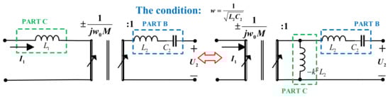
Figure 17.
The equivalent model of the I_CC_CV circuit.
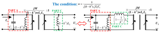
Figure 18.
The equivalent model of the II_CC_CV circuit.
Figure 19.
The equivalent model of the III_CC_CV circuit.
4. Source-Side or Load-Side Conversion Model
Source-side or load-side conversion model converts voltage to current at the source/load side using LC/CL resonant tank or converts current to voltage at the source/load side using LC/CL resonant tank. Therefore, depending on the direction of the transition, there are two types of source-/load-side conversion circuits as shown in Figure 20 and Figure 21. The first type converts a constant voltage into a constant current, while the second type does the opposite. The resonant angular frequency of the resonant tank consisting of the inductor LR and the capacitor CR is equal to the angular frequency ω of the sinusoidal voltage source Uin and current source Iin. Therefore, according to Norton equivalent
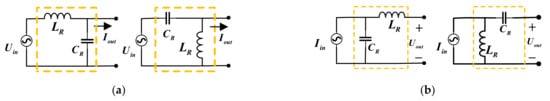
Figure 20.
(a) Voltage to current at source side (I_S); (b) current to voltage at source side (II_S).
Figure 21.
(a) Voltage to current at load side (I_L); (b) Current to voltage at load side (II_L).
In accordance with (13a) and (13b), if Uin/Iin is constant, the output current/voltage of the LC/CL resonant tank (Iout/Uout) is constant as well.
5. Compensation Topology Design Method for IPT System
The design methodology for voltage-fed compensation circuit with load-independent CC/CV output at ZPA frequencies is given in detail below. It should be noted that the design method presented in this paper can be easily transplanted to the comprehensive design of the current-fed compensation network.
Take voltage-source driving to realize load-independent CC output as an example to illustrate the design method of this article. Combining with the model analysis in Section 3 and Section 4, there can be three types of design forms as shown in Figure 22.
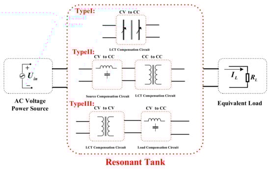
Figure 22.
Design diagram for CC output in IPT systems.
- The first type is direct conversion, that is, the CV_CC model of Section 3.2.
- The second type uses the LC/CL resonant tank at the source side to convert voltage to the current, and then the CC_CC model is used to convert to constant current.
- The third type uses the CV_CV model to convert voltage to voltage, and the LC/CL resonant tank at the load side is used to convert the voltage to constant current.
The first type (D_CV_CC): The voltage source cannot drive the parallel topology [6]; therefore, the I_CV_CC model cannot be directly used to achieve constant voltage to constant current from the source to load. In order to achieve ZPA characteristics, the compensation capacitor can be connected in series on the secondary side of the II_CV_CC/III_CV_CC model, as shown in Figure 23. The ZPA realization condition is
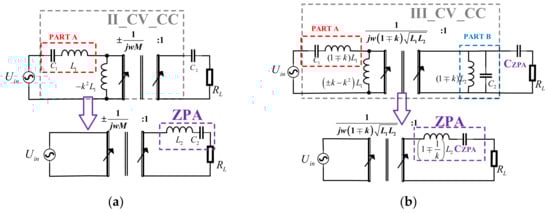
Figure 23.
The D_CV_CC type compensation topology: (a) S/S [14,15,21,22,23] and (b) S/PS [15].
In terms of the current-voltage conversion characteristics of an ideal gyrator, the value of the load-independent transconductance () of Figure 23 is expressed as
A is the transfer ratio of the ideal gyrator.
The second type (S_CC_CV): As described above, the source conversion circuits have two options, and the CC_CC model has three types. There is a total of seven design forms as shown in Figure 24. Among them, LCL/P [21,22,24,25,26], LCC/P [15,21,25], CLC/P [21], LC /S [27], and LCL/P [26] have all been analyzed in detail in the previous researches. Two new topologies are designed, namely LC and CLC/S compensation topology. The following seven design forms of ZPA implementation conditions can be converted into the circuits shown in Figure 23 and Figure 24a. The Z parameter matrix corresponding to the two-port network in the red box is , Then, the port input impedance is . is the load resistance equivalent to the resistance of the primary stage, which can be expressed as
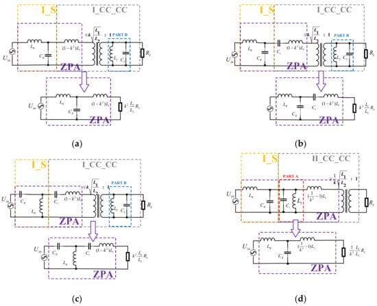
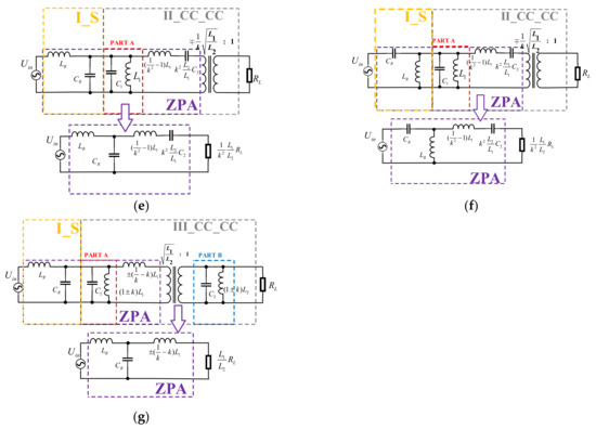
Figure 24.
The S_CC_CC compensation topologies: (a) LCL/P [21,22,24,25,26]; (b) LCC/P [15,21,25]; (c) CLC/P [21]; (d) LC; (e) LC/S [27]; (f) CLC/S; and (g) LCL/P [26].
A is the ratio of the primary voltage to the secondary voltage of an ideal transformer in Figure 25a. The conditions for the constant-current output of the S_CC_CV type circuit are resulting in Z11 = 0. Z12 and Z21 are inductive or capacitive components, which result in not containing imaginary parts. Therefore, in order to make Zin a pure resistance, the conditions for the establishment of ZPA are
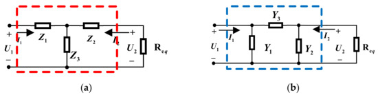
Figure 25.
(a) The zero-phase angle (ZPA) condition of S_CC_CC compensation topology and (b) The ZPA condition of CV_CV_L compensation topology.
According to (18), the ZPA conditions of LC and CLC/S compensation topology are
The ZPA implementation conditions of other topologies are shown in Table 3.
Table 3.
The design results for voltage-fed compensation circuit with load-independent CC output at ZPA frequencies.
The load-independent transconductance () of Figure 24 is expressed as
The third type (CV_CV_L): As described above, the CV_CV model has three types, and the load conversion circuits have two options. Four novel compensation topologies are designed as shown in Figure 26: namely, S/LC, S/LCC, S/CLC, and S/LC. The above compensation topologies of ZPA implementation conditions can be converted into the circuits shown in Figure 25b and Figure 26. The Y parameter matrix corresponding to the two-port network in the blue box is . Then, the port input impedance is . Similarly, the ZPA realization conditions are
Figure 26.
The CV_CV_L compensation topologies: (a) S/LC; (b) S/LCC; (c) S/CLC; (d) S/LC.
The ZPA implementation conditions of the above compensation topologies are shown in Table 3.
The load-independent transconductance () of Figure 26 is expressed as:
There are similar design methods for the voltage-fed high-order resonant network to realize load-independent constant-voltage output. The specific design process can be seen in Figure 27, Figure 28 and Figure 29. Detailed design results are shown in Table 4.
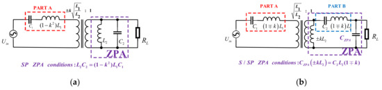
Figure 27.
The D_CV_CV compensation topologies: (a) SP [5,14,15,28] and (b) S/SP [6,14,16,17,29,30].
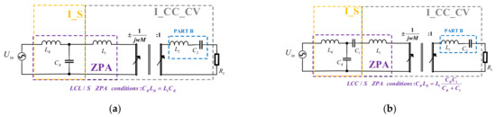
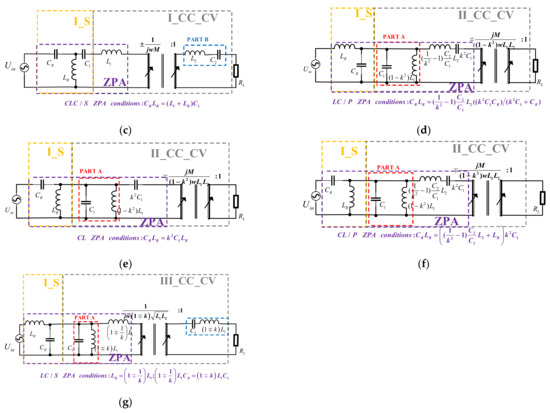
Figure 28.
The S_CC_CV compensation topologies: (a) LCL/S [22]; (b) LCC/S [6,15,16,17,31,32]; (c) CLC/S; (d) LC/P; (e) CL; (f) CL/P; and (g) LC/S [12].
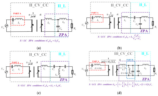
Figure 29.
The CV_CC_L compensation topologies: (a) S/LC; (b) S/LCC; (c) S/CLC [12]; and (d) S/LCL [33].
Table 4.
The design results for voltage-fed compensation circuit with load-independent CV output at ZPA frequencies.
As shown in Table 3 and Table 4, for compensation topologies with less than three compensation elements, including S/S compensation, S/PS compensation, S/P compensation, and S/SP compensation, they all have LCT-constrained transfer functions, which means that once the input voltage is determined, the output voltage or current of the system is changed unless the LCT is replaced. However, many applications such as implanted devices have this strict limit on the size of the system space, making that the design of LCT is generally space limited. Therefore, it is difficult to design an LCT to meet all the requirements. Besides, the redesign of LCT is both time and cost consuming.
Compared to these compensation topologies, six novel compensation topologies with LCT-unconstrained CC output characteristics including LC, CLC/S, S/LC, S/LCC, S/CLC, and S/LC and six novel compensation topologies with LCT-unconstrained CV output characteristics including CLC/S, LC/P, CL, CL/P, S/LC, and S/LCC are designed as listed in Table 3 and Table 4. It is clear to see that the input–output transfer functions of these compensation topologies depend not only on the parameters of the LCT but also on the value of LR, which reveals the fact that the output voltage or current can be changed by changing the value of LR without replacing a new LCT, thus freeing the design from the constraints imposed by the LCT parameters.
In addition, these topologies only require less than four compensation elements, compared to the six compensation elements required for the double-side LCC compensation topology, resulting in a smaller system size, higher power density, and lower cost.
6. Simulation and Experimental Verification
6.1. Simulation Verification
In this section, the novel compensation topologies with constant-current output characteristics including LC, CLC/S, S/LC, S/LCC, S/CLC, and S/LC circuits are simulated to verify the ZPA and constant-current output characteristics. The mathematical model of the above compensation topologies is established in MATLAB for simulation. For all the compensation topology, the simulation conditions are the same, including the inductance of the primary and secondary coils which are 6.71 μH and 6.68 μH, respectively. The coupling coefficient k is 0.1, the operating frequency of the circuit system is 200 kHz, and the load resistors RL ranges from 100 Ω to 1000 Ω. The parameter designs of compensation topology are referred to Table 3. The transfer ratio of the above compensation circuits and the phase-frequency characteristic curve of the input impedance obtained by simulation are shown in Figure 30. It can be seen that only the input impedances at the fully compensated frequency (200 kHz) are purely resistive. In addition, the transfer ratio corresponding to this point is independent of the load value, which verifies the theoretical analysis and the designed parameters shown in Table 3.
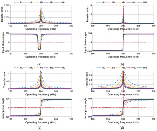
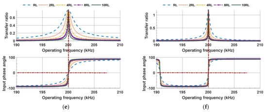
Figure 30.
Transfer ratio and phase angle of the input impedance simulation results for (a) LC, (b) CLC/S, (c) S/LC, (d) S/LCC, (e) S/CLC, and (f) S/LC topologies versus operating frequency.
Similarly, the compensation topology with constant-voltage output characteristics including CLC/S, LC/P, CL, CL/P, S/LC, and S/LCC circuits are also simulated. The parameter designs of compensation circuits are referred to in Table 4. The simulation results in Figure 31 are also consistent with the theoretical analysis.
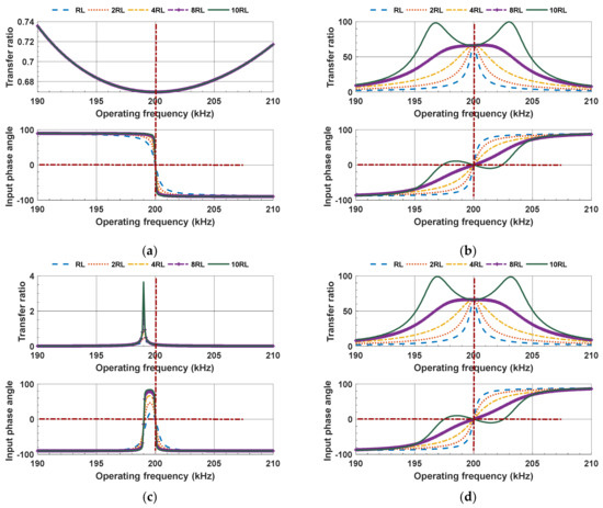
Figure 31.
Voltage transfer ratio and phase angle of the input impedance simulation results for: (a) CLC/S; (b) LC/P; (c) CL; (d) CL/P; (e) S/LC; and (f) S/LCC topologies versus operating frequency.
6.2. Experimental Results
In order to further verify theoretical analysis, a S/LCC compensation network in an IPT system is constructed as shown in Figure 32 and realized on the printed circuit board (PCB) as shown in Figure 33. Q1~Q4 are primary-side power MOSFETs that constitute a full-bridge inverter. L1 and L2 are the self-inductances of primary and secondary coils, respectively. The values of L1 and L2 are fixed at 6.97 μH and 6.98 μH, respectively. C1 is the series compensation capacitor of the primary side. C2, CR, and LR are the series compensation capacitor, the parallel compensation capacitor, and the series inductor of the second side. D1~D4 are the rectifier diodes at the secondary side that form a full bridge rectifier. CRec is the filter capacitor, and RL is the practical load. When the distance between the two coils is 3.5 cm, the coupling coefficient is measured as 0.1. We selected the resonant frequency of 200 kHz and the values of LR to be 1.44 μH and designed the values of compensation capacitors according to Figure 29b and Table 4. The measured values of compensation capacitance and other circuit parameters are shown in Table 5.
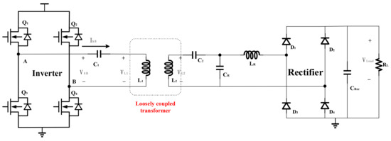
Figure 32.
S/LCC compensation topology in IPT system.
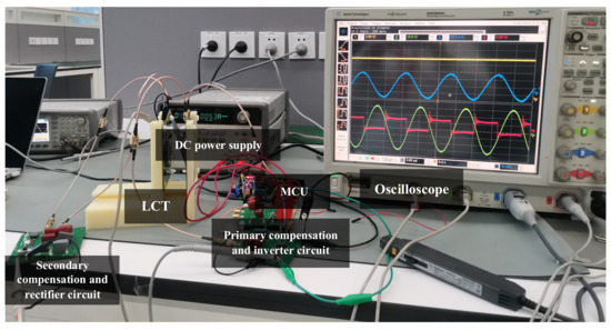
Figure 33.
S/LCC compensated IPT prototype.
Table 5.
Circuit parameters of S/LCC compensation topology.
Figure 34 is the voltage waveforms of the primary coil and the secondary coil. Figure 35 shows the waveforms of the inverter output voltage VAB and current IAB. It can be seen from the Figure that the phase of VAB and IAB are basically the same. The experimental results of inverter output voltage VAB and transmitter coil voltage VL1 are shown in Figure 36. The phase difference between VAB and VL1 is 90°. The above two experimental results both prove that the system achieves ZPA characteristics.
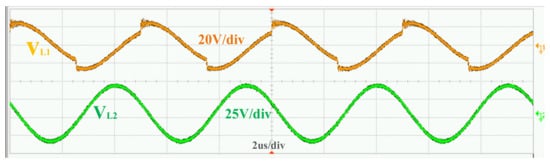
Figure 34.
Transmitter coil voltage VL1 and receiving coil voltage VL2.
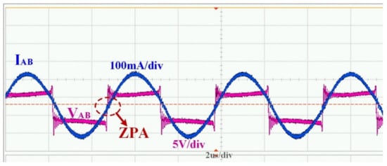
Figure 35.
Inverter output voltage VAB and current IAB when ZPA.
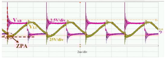
Figure 36.
Inverter output voltage VAB and transmitter coil voltage VL1 when ZPA.
As mentioned in Section 1, in order to achieve soft switching, the circuit should be slightly inductive. When the C1 is adjusted to 101.16 nF, the measured VAB and IAB are shown in Figure 37. It can be seen that the phase of the voltage leads the current by about 30°, and the circuit realizes the ZVS characteristic.
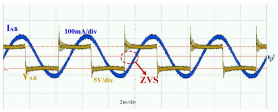
Figure 37.
Inverter output voltage VAB and current IAB when ZVS.
Figure 38 shows the output voltage waveform of the system when the load is suddenly changed. When the load resistance RL drops suddenly from 1000 Ω to 100 Ω, the voltage on the load drops from 7.91 V to 6.89 V. When the load resistance is 100 Ω, the system efficiency is 88.6%. When the load drops by 10% on average, the output voltage only decreases by 1.42%. Therefore, the system can still be regarded as a constant-voltage output system. Although the theoretical analysis proves that the load voltage does not change with the change of the load resistance, it should be noted that the theoretical analysis did not consider the influence of factors such as parasitic resistance and parameter errors in the real system. In addition, the simulation proves that if the series resistances of the coil and the capacitor and the on-resistances of the power MOSFETs are considered, the resistance voltage changes slightly with the change of resistance. Therefore, the constant-voltage characteristic of S/LCC compensation topology is significantly improved if devices with higher accuracy and smaller parasitic resistances are used.
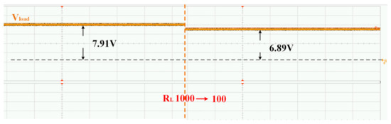
Figure 38.
The output voltage VLoad of the system when the load is suddenly changed.
6.3. Discussion of the Experimental Results
Based on the above experimental results, we get the following: at zero-phase angle frequency, the equivalent impedance of the S/LCC circuit is a pure resistance, minimizing the VA ratings; on the basis of the realization of ZPA characteristics, it is very convenient and easy to implement ZVS just by slightly changing the value of the primary compensation capacitor; the S/LCC has excellent constant-voltage characteristics; and the load changes in a large range while the output-constant voltage is almost unchanged, which simplifies the design of the system control circuit.
7. Discussion
Table 6 shows the comparisons of the design method in this paper with other literature. Based on Table 6, we can get that the proposed design approach in this work is suitable for practical use due to its intuitive, comprehensive, and innovative aspects for the following reasons:
Table 6.
Comparison with previous works.
- It is intuitive because compared to the previous literature which used mathematical methods, the proposed design method can be carried out with graphical steps without complex equation calculations. The load-independent frequency, ZPA conditions, and source-to-load voltage/current gain of the compensation topology can be obtained almost by inspection conveniently, giving a new perspective that is free from the constraints of complex equations;
- It is comprehensive because unlike the other literature that focuses on the analysis of existing compensation topologies, the compensation topologies designed according to our method not only include some compensation structures in the previous researches but also include some new compensation circuits that have never been proposed before;
- It is innovative because unlike the modeling methods of compensation topology in previous literature, in this paper, LCT is modeled as four forms of circuits based on the ideal gyrator and transformer under different input and output conditions, giving fruitful insights that are not constrained by complex formulaic calculations. Moreover, on the basis of the design methodology in this paper, twelve novel compensation topologies with LCT-unconstrained CC or CV output are stated. They all have the input-to-output transfer function independent of LCT parameters to get higher design freedom compared to conventional compensation topology and fewer compensation components compared to double-sided LCC compensation topology to obtain a lower cost, less space, and higher power density.
8. Conclusions
In this paper, a simple, comprehensive, and innovative graphical design methodology is proposed for designing compensation circuits to realize load-independent CV or CC output at zero-phase angle (ZPA) frequencies. The proposed approach can be applied to design a set of high-order compensation topologies in a consistent manner. Unlike boring and time-consuming design methods for manipulating circuit equations, using the circuit model given in this paper the load-independent frequency, ZPA conditions, and source-to-load voltage/current gain of the compensation topology can be obtained almost by inspection conveniently, giving a new perspective being free from the constraints of complex equations. Unlike design methods that focus on the analysis of existing compensation topologies, by virtue of the design method in this paper, twelve novel compensation topologies having the input-to-output transfer functions independent of LCT parameters and load-independent CC/CV output are designed and simulated. An S/LCC-compensated IPT system fed by a voltage source with load-independent CV output is designed and manufactured in accordance with the design method of this paper. Simulation and experimental results have shown excellent agreement with the theory. This paper focuses on the compensation topology with constant current or constant voltage under the condition that the coupling coefficient is constant but the load fluctuates greatly, which is suitable for static wireless charging systems with a fixed position. Our future research direction will research the capability of misalignment tolerance of different compensation topologies with load-independent outputs, that is, the sensitivity of the output voltage or current to the change of the coupling coefficient, which will be applied to dynamic wireless power transfer systems.
Author Contributions
Conceptualization, Q.S., Y.L. (Yan Li), X.W., and X.L.; methodology, Q.S., Y.L. (Yan Li), X.L., and Z.W.; software, Q.S., X.W., and Y.L. (Yan Li); formal analysis, Q.S., X.L., and Y.L. (Yan Li); writing—original draft preparation, Q.S.; writing—review and editing, Q.S., X.L., Y.L. (Yan Li), and Z.W; supervision, Y.L. (Yu Liu). All authors have read and agreed to the published version of the manuscript.
Funding
This research was funded by National Key R&D Program of China under grant number 2019YFB2204900: 2019YFB2204500, 2018YFC2001103.
Conflicts of Interest
The authors declare no conflict of interest.
References
- Mahdi, A.J.; Fahad, S.; Tang, W. An Adaptive Current Limiting Controller for a Wireless Power Transmission System Energized by a PV Generator. Electronics 2020, 9, 1648. [Google Scholar] [CrossRef]
- Wen, F.; Chu, X.; Li, Q.; Gu, W. Compensation Parameters Optimization of Wireless Power Transfer for Electric Vehicles. Electronics 2020, 9, 789. [Google Scholar] [CrossRef]
- Gati, E.; Kokosis, S.; Patsourakis, N.; Manias, S. Comparison of Series Compensation Topologies for Inductive Chargers of Biomedical Implantable Devices. Electronics 2019, 9, 8. [Google Scholar] [CrossRef]
- Jegadeesan, R.; Guo, Y.-X. Topology Selection and Efficiency Improvement of Inductive Power Links. IEEE Trans. Antennas Propag. 2012, 60, 4846–4854. [Google Scholar] [CrossRef]
- Qu, X.; Jing, Y.; Han, H.; Wong, S.-C.; Tse, C.K. Higher Order Compensation for Inductive-Power-Transfer Converters With Constant-Voltage or Constant-Current Output Combating Transformer Parameter Constraints. IEEE Trans. Power Electron. 2017, 32, 394–405. [Google Scholar] [CrossRef]
- Lu, J.; Zhu, G.; Wang, H.; Lu, F.; Jiang, J.; Mi, C.C. Sensitivity Analysis of Inductive Power Transfer Systems With Voltage-Fed Compensation Topologies. IEEE Trans. Veh. Technol. 2019, 68, 4502–4513. [Google Scholar] [CrossRef]
- Shang, Y.; Liu, K.; Cui, N.; Wang, N.; Li, K.; Zhang, C. A Compact Resonant Switched-Capacitor Heater for Lithium-Ion Battery Self-Heating at Low Temperatures. IEEE Trans. Power Electron. 2020, 35, 7134–7144. [Google Scholar] [CrossRef]
- Liu, K.; Yang, Z.; Tang, X.; Cao, W. Automotive Battery Equalizers Based on Joint Switched-Capacitor and Buck-Boost Converters. IEEE Trans. Veh. Technol. 2020, 69, 12716–12724. [Google Scholar] [CrossRef]
- Ouyang, Q.; Wang, Z.; Liu, K.; Xu, G.; Li, Y. Optimal Charging Control for Lithium-Ion Battery Packs: A Distributed Average Tracking Approach. IEEE Trans. Ind. Inform. 2020, 16, 3430–3438. [Google Scholar] [CrossRef]
- Liu, K.; Zou, C.; Li, K.; Wik, T. Charging Pattern Optimization for Lithium-Ion Batteries With an Electrothermal-Aging Model. IEEE Trans. Ind. Inform. 2018, 14, 5463–5474. [Google Scholar] [CrossRef]
- Huang, C.; Kawajiri, T.; Ishikuro, H. A 13.56-MHz Wireless Power Transfer System With Enhanced Load-Transient Response and Efficiency by Fully Integrated Wireless Constant-Idle-Time Control for Biomedical Implants. IEEE J. Solid-State Circuits 2018, 53, 538–551. [Google Scholar] [CrossRef]
- Yao, Y.; Wang, Y.; Liu, X.; Xu, D. Analysis, Design, and Optimization of LC/S Compensation Topology With Excellent Load-Independent Voltage Output for Inductive Power Transfer. IEEE Trans. Transp. Electrif. 2018, 4, 767–777. [Google Scholar] [CrossRef]
- Li, S.; Li, W.; Deng, J.; Nguyen, T.D.; Mi, C.C. A Double-Sided LCC Compensation Network and Its Tuning Method for Wireless Power Transfer. IEEE Trans.Veh. Technol. 2015, 64, 2261–2273. [Google Scholar] [CrossRef]
- Zhang, W.; Siu-Chung, W.; Tse, C.K.; Qianhong, C. Load-Independent Duality of Current and Voltage Outputs of a Series- or Parallel-Compensated Inductive Power Transfer Converter With Optimized Efficiency. IEEE J. Emerg. Sel. Top. Power Electron. 2015, 3, 137–146. [Google Scholar] [CrossRef]
- Zhang, W.; Mi, C.C. Compensation Topologies of High-Power Wireless Power Transfer Systems. IEEE Trans. Veh. Technol. 2016, 65, 4768–4778. [Google Scholar] [CrossRef]
- Lu, J.; Zhu, G.; Lin, D.; Wong, S.-C.; Jiang, J. Load-Independent Voltage and Current Transfer Characteristics of High-Order Resonant Network in IPT System. IEEE J. Emerg. Sel. Top. Power Electron. 2019, 7, 422–436. [Google Scholar] [CrossRef]
- Lu, J.; Zhu, G.; Lin, D.; Zhang, Y.; Jiang, J.; Mi, C.C. Unified Load-Independent ZPA Analysis and Design in CC and CV Modes of Higher Order Resonant Circuits for WPT Systems. IEEE Trans. Transp. Electrif. 2019, 5, 977–987. [Google Scholar] [CrossRef]
- Sohn, Y.-H.; Choi, B.; Cho, G.-H.; Rim, C. Gyrator-Based Analysis of Resonant Circuits in Inductive Power Transfer Systems. IEEE Trans. Power Electron. 2015. [Google Scholar] [CrossRef]
- Chwei-Sen, W.; Covic, G.A.; Stielau, O.H. Power transfer capability and bifurcation phenomena of loosely coupled inductive power transfer systems. IEEE Trans. Ind. Electron. 2004, 51, 148–157. [Google Scholar] [CrossRef]
- Tellegen, B.D.H. The gyrator, A new electric network element. Philips Res. 1948, 3, 81. [Google Scholar]
- Hou, J.; Chen, Q.; Zhang, Z.; Wong, S.; Tse, C.K. Analysis of Output Current Characteristics for Higher Order Primary Compensation in Inductive Power Transfer Systems. IEEE Trans. Power Electron. 2018, 33, 6807–6821. [Google Scholar] [CrossRef]
- Qu, X.; Han, H.; Wong, S.-C.; Tse, C.K.; Chen, W. Hybrid IPT Topologies With Constant Current or Constant Voltage Output for Battery Charging Applications. IEEE Trans. Power Electron. 2015, 30, 6329–6337. [Google Scholar] [CrossRef]
- Zhang, W.; Wong, S.-C.; Tse, C.K.; Chen, Q. Analysis and Comparison of Secondary Series- and Parallel-Compensated Inductive Power Transfer Systems Operating for Optimal Efficiency and Load-Independent Voltage-Transfer Ratio. IEEE Trans. Power Electron. 2014, 29, 2979–2990. [Google Scholar] [CrossRef]
- Fang, L.; Zhang, Y.; Chen, K.; Zhao, Z.; Liqiang, Y. A comparative study of load characteristics of resonance types in wireless transmission systems. In Proceedings of the 2016 Asia-Pacific International Symposium on Electromagnetic Compatibility (APEMC), Shenzhen, China, 17–21 May 2016; pp. 203–206. [Google Scholar]
- Li, W.; Zhao, H.; Kan, T.; Mi, C. Inter-operability considerations of the double-sided LCC compensated wireless charger for electric vehicle and plug-in hybrid electric vehicle applications. In Proceedings of the 2015 IEEE PELS Workshop on Emerging Technologies: Wireless Power (2015 WoW), Daejeon, Korea, 5–6 June 2015; pp. 1–6. [Google Scholar]
- Yao, Y.; Liu, X.; Wang, Y.; Xu, D. Modified parameter tuning method for LCL/P compensation topology featured with load-independent and LCT-unconstrained output current. Iet Power Electron. 2018, 11, 1483–1491. [Google Scholar] [CrossRef]
- Wang, Y.; Yao, Y.; Liu, X.; Xu, D.; Cai, L. An LC/S Compensation Topology and Coil Design Technique for Wireless Power Transfer. IEEE Trans. Power Electron. 2018, 33, 2007–2025. [Google Scholar] [CrossRef]
- Huang, Z.; Wong, S.; Tse, C.K. Design methodology of a series-series inductive power transfer system for electric vehicle battery charger application. In Proceedings of the 2014 IEEE Energy Conversion Congress and Exposition (ECCE), Pittsburgh, PA, USA, 14–18 September 2014; pp. 1778–1782. [Google Scholar]
- Hou, J.; Chen, Q.; Ren, X.; Ruan, X.; Wong, S.; Tse, C.K. Precise Characteristics Analysis of Series/Series-Parallel Compensated Contactless Resonant Converter. IEEE J. Emerg. Sel. Top. Power Electron. 2015, 3, 101–110. [Google Scholar] [CrossRef]
- Hou, J.; Chen, Q.; Yan, K.; Ren, X.; Wong, S.; Tse, C.K. Analysis and control of S/SP compensation contactless resonant converter with constant voltage gain. In Proceedings of the 2013 IEEE Energy Conversion Congress and Exposition, Denver, CO, USA, 15–19 September 2013; pp. 2552–2558. [Google Scholar]
- Zhang, H.; Chen, Y.; Park, S.-J.; Kim, D.-H. A Hybrid Compensation Topology With Single Switch for Battery Charging of Inductive Power Transfer Systems. IEEE Access 2019, 7, 171095–171104. [Google Scholar] [CrossRef]
- Chen, S.; Chen, Y.; Li, H.; Dung, N.A.; Mai, R.; Tang, Y.; Lai, J.-S. An Operation Mode Selection Method of Dual-Side Bridge Converters for Efficiency Optimization in Inductive Power Transfer. IEEE Trans. Power Electron. 2020, 35, 9992–9997. [Google Scholar] [CrossRef]
- Wang, Y.; Yao, Y.; Liu, X.; Xu, D. S/CLC Compensation Topology Analysis and Circular Coil Design for Wireless Power Transfer. IEEE Trans. Transp. Electrif. 2017, 3, 496–507. [Google Scholar] [CrossRef]
Publisher’s Note: MDPI stays neutral with regard to jurisdictional claims in published maps and institutional affiliations. |
© 2021 by the authors. Licensee MDPI, Basel, Switzerland. This article is an open access article distributed under the terms and conditions of the Creative Commons Attribution (CC BY) license (http://creativecommons.org/licenses/by/4.0/).