Abstract
Wearable medical devices, wireless sensor networks, and other energy-constrained sensing devices are often concerned with finding specific data within more-complex signals while maintaining low power consumption. Traditional analog-to-digital converters (ADCs) can capture the sensor information at a high resolution to enable a subsequent digital system to process for the desired data. However, traditional ADCs can be inefficient for applications that only require specific points of data. This work offers an alternative path to lower the energy expenditure in the quantization stage—asynchronous content-dependent sampling. This asynchronous sampling scheme is achieved by pairing a flexible analog front-end with an asynchronous successive-approximation ADC and a time-to-digital converter. The versatility and reprogrammability of this system allows a multitude of event-driven, asynchronous, or even purely data-driven quantization methods to be implemented for a variety of different applications. The system, fabricated in standard 0.5 m and 0.35 m processes, is demonstrated along with example applications with voice, EMG, and ECG signals.
1. Introduction
Whether the application is bio-signal monitoring with wearable devices, voice-activity detection by an Internet-of-Things device, or data logging with wireless-sensor-network nodes, modern electronics require application-specific data capture with as low a power budget as possible. The means that are used to sample and preprocess (usually compress) a signal comprise a major part of this power budget. Traditional analog-to-digital converters have made great strides in power efficiency, but their sampling rate is constrained by the Nyquist–Shannon sampling theorem. This rigid sampling-rate criteria can create a large amount of sample overhead in signals with varying frequency content, which manifests as extraneous power expenditure in the quantization, processing, and transmission stages.
This work offers an alternative path to lower energy expenditure in the quantization stage—content-dependent sampling of a signal. Instead of sampling at a constant rate, the demonstrated system asynchronously produces two digital signals—one proportional to the sample amplitude and the other proportional to the intersample time period, as shown in Figure 1. The trigger mechanism for these data-driven asynchronous measurements is controlled by an analog front-end implemented in our reconfigurable analog/mixed-signal platform (RAMP) system [1]. The use of a reconfigurable front-end allows us to create a sample triggering mechanism tuned to the minimal amount of required data for a given application. The well-tuned analog front-end, combined with asynchronous data conversion, allows for highly efficient data extraction. This work is an extension of our earlier work presented in [2], which demonstrated the promise of an asynchronous ADC coupled with analog preprocessing. Here, we provide further circuit details, a discussion on a sampling method that works in conjunction with asynchronous conversion, and additional example applications.
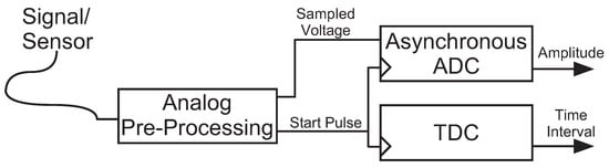
Figure 1.
Asynchronous analog-to-digital conversion system. A reconfigurable analog front-end reduces information to only the relevant data points and also triggers the subsequent blocks, which produce digital words for the corresponding voltages and time intervals.
This work demonstrates the use of a fabricated RAMP and an asynchronous ADC to convert the minimal number of samples required to either recreate a signal or optimally extract specific data from a signal. An overview of asynchronous conversion is presented in Section 2. Section 3 establishes the overall system architecture that we use to implement our adaptive sampling technique, including a discussion of our reconfigurable analog front-end and the data conversion circuits. Section 4 describes the asynchronous triggering process in this conversion system that allows for only the local maxima/minima to be sampled. Section 5 demonstrates example uses of the system in voice, electromyography (EMG), and electrocardiogram (ECG) monitoring environments, before concluding in Section 6.
2. Asynchronous Quantization
The most traditional path to achieving a reduction in energy expenditure of electronic devices is through the scaling of the minimum feature size of the transistors, which primarily benefits digital systems. Unfortunately, the conversion of an analog signal into a digital one is an inherently mixed-signal process. The analog portions of this process tend to suffer as transistor dimensions scale, due to the increased device mismatch and the lower voltage overhead (from reduced supply voltages). While there are techniques meant to mitigate these issues [3], process-scaling is usually not the simplest or most cost-effective means of reducing energy expenditure in the quantization stage.
The next direct path toward reducing the power expended on sampling a signal is to reduce the number of samples taken. The Walden figure of merit for analog-to-digital converters (ADCs) suggests that, for ADCs of comparable resolution, a reduction in power can be achieved through an equal reduction in sampling rate [4]. Unfortunately, traditional Nyquist–Shannon sampling sets the sampling rate at a hard minimum of twice the highest frequency content of a signal. While fixed-rate sampling has the advantage of being very-well understood and characterized, it does not provide an efficient means of sampling sparse or ‘bursty’ signals—signals characterized by relatively short periods of high activity and potentially long periods of inactivity (e.g., voice-control systems).
The extraneous quantization of signals creates increased energy overhead outside of the quantization stage as well. For these quantized signals to be useful, they must normally be processed by a microcontroller and/or transmitted to some other device by a transceiver. Logically, the more samples that are taken, the more samples that must be processed and transmitted by the microcontroller/transceiver. This has a compounding effect on the power consumption, as these activities reduce the amount of time it may stay in a low-power ‘sleep’ state, which operates at orders-of-magnitude lower power expenditure than the active state. For context, the active states of two low-power industry-standard components, the MSP430 microcontroller and the CC110L transceiver, consume over 200 times and 80,000 times more current than their respective sleep states [5]. It is, therefore, very desirable to leave these devices in a sleep-state as much as possible by reducing the sample overhead.
The desire to vary a data converter’s sampling rate so that it may adapt to the changing frequency characteristics of a signal has given rise to data converters that rely on asynchronous sampling methods. Instead of wasting a significant amount of energy converting parts of the signal that contain relatively little data, asynchronous sampling methods base their rate on the signal itself. The trigger for these methods can be a number of different signal-characterization or classification circuits, but many asynchronous sampling solutions struggle with a robustness/resolution trade-off.
Level-crossing ADCs are possibly the most popular type of asynchronous ADCs [6,7,8,9]. The basic concept is that a sample is only converted when the measured signal passes through a bound that would represent a new digital word. By only recording these transitions, periods of relative inactivity are ignored. Ignoring these inactive periods allows energy to be saved through reducing the number of conversions [10]. While this method avoids extraneous conversions during periods of low-activity, level-crossing ADCs have a severe resolution–bandwidth trade-off—the higher the resolution of the ADC, the longer it takes for large-amplitude high-frequency content to traverse through the many quantization levels.
Alternative triggering schemes can be made from analog front-ends designed for different signal-conditioning and classification schemes. For example, one could imagine an ADC triggered upon the detection of a certain frequency within a signal [11] or upon the detection of vocal characteristics of a signal [12]. Indeed, many energy-efficient analog front-ends [13] could provide a trigger for an asynchronous data converter. Unfortunately, these analog circuits are very application-specific, requiring new circuits to be designed on a per-application basis.
The desire to enable reconfigurability in analog electronics has led to the development of a relatively new class of devices called field-programmable analog arrays (FPAAs) [1,14,15,16]. FPAAs are similar to digital field-programmable gate arrays (FPGAs) in that they allow for a system architect to program arbitrary connections of primitives to form larger systems. Allowing circuit designers to reconfigure and retune analog elements and biases allow these FPAAs to function across a myriad of applications. In this work, we leverage our reconfigurable analog front-end—the RAMP—to provide user-defined triggers to enable conversion based upon the characteristics of the signal, thereby minimizing the number of conversions to significantly save power.
3. System Overview
When sampling signals with sparse information, constant-rate sampling unavoidably creates extraneous samples during periods of low activity. These extraneous samples create waste in the quantization stage as well as further down the signal-processing chain in the microcontroller and transceiver stages. The use of analog preprocessing has been shown to be computationally efficient to find the data points needing to be converted [13]. While a fully custom front-end would yield the highest energy savings, the use of a field-programmable analog array allows us to adapt the front-end for a variety of applications.
Once the FPAA-synthesized analog front-end detects some predefined characteristic of the signal, it calls for the immediate quantization of the signal. Due to the asynchronous nature of the quantization, not only must the amplitude be recorded, but the time interval since the last sampling event must also be recorded, as shown in Figure 1.
The amplitude conversion within the demonstrated system occurs with a simple successive-approximation analog-to-digital converter. From a system perspective, the unique aspect of this ADC is that it must be triggered to initiate conversion. This trigger signal also activates a time-to-digital converter (TDC). A TDC is essentially an oscillator with a digital counter attached to the output that counts the number of oscillations between extrema occurrences. By pausing/resetting the TDC after every sample, the total number of counted oscillations will be proportional to the elapsed time since the previous sample, thus enabling intersample time measurement. The constant oscillation of the TDC may seem inefficient, but a unique feature of this system is that the ADC uses the TDC as its required clock signal. By replacing the system clock, the TDC offsets some of its own power budget within the system.
3.1. Reconfigurable Analog Mixed-Signal Platform
The reconfigurable analog/mixed-signal platform (RAMP) refers to our FPAA, which is capable of synthesizing large and complex circuits for event-driven and signal-processing designs. Coupled with a custom netlist-based language and place-and-route routines, the RAMP enables users without circuit-level expertise to quickly develop applications in silicon [1].
As shown in Figure 2, the RAMP contains 80 computational analog blocks (CABs) that are interconnected via ten stages with eight channels. The ten stages are organized by processing type, such as basic circuit elements (e.g., transistors and capacitors), transconductors, continuous-time filters, mixed-signal operations, etc. The eight identical channels provide the ability to create parallelized designs, as needed. Moreover, many of the synthesizable elements are tunable to set desired performance parameters (e.g., gain, filter corner frequency, etc.) and to tailor the respective circuit to the input signal characteristics. This tunable functionality is provided by floating-gate transistors, which are described in more detail in [17].
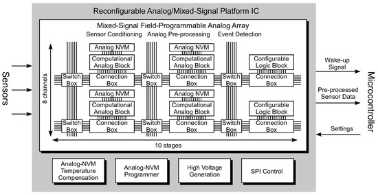
Figure 2.
Architecture of the reconfigurable analog/mixed-signal platform (RAMP) integrated circuit.
3.2. Asynchronous Data Converter Design
The voltage amplitude conversion of the asynchronously sampled values is performed by a successive-approximation ADC (SA-ADC). The successive-approximation architecture was chosen for its demonstrated power efficiency [18]. It also has the advantage of being appropriate for a relatively large range of frequencies and amplitudes, thus making it an appropriate choice for a variety of different systems with varying signal characteristics. The following discussion is devoted to the specific circuits shown in Figure 3 that give this ADC its functionality including the successive-approximation register, comparator, and time-to-digital converter.
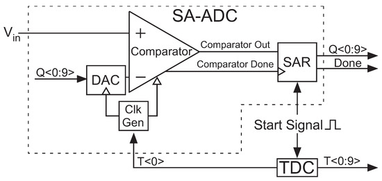
Figure 3.
System diagram of the successive-approximation ADC (SA-ADC)/time-to-digital converter (TDC). A trigger from the RAMP analog preprocessing stage acts as the ‘Start Signal’ to initiate conversion and record the time.
3.2.1. Successive-Approximation Register
The successive-approximation register (SAR), which is shown in Figure 4, is the control circuitry used to run the binary-search-like process within an SA-ADC. The basic principle of this search is to test each bit from the MSB to the LSB and save the result. The boxed top half of Figure 4 is simply a shift register. This portion of the SAR passes a logic high down the chain of flip-flops upon each clock cycle, which is provided by the ‘Comparator Done’ signal, as shown in Figure 3. When a flip-flop in the shift register outputs a logic high, a corresponding flip-flop below it is also set high. This bottom row of flip-flops applies the digital word to the digital-to-analog converter (DAC) that provides the voltage to which the input is compared. When the next shift occurs, but before the DAC or comparator is updated, the previous bit is changed to reflect the output of the comparator. Logically, this is the equivalent of the flip-flop updating its output to reflect whether the guess was accurate or not. This process proceeds in a sequential manner until the last flip-flop outside of the dashed box on the top row receives the logic high—this event signifies that the SAR has finished all of its cycles, and thus the analog-to-digital conversion is complete. The SAR implemented in this work is 10 bits.
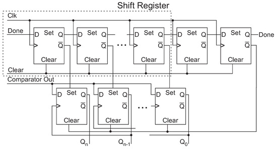
Figure 4.
A schematic of the successive approximation register. The boxed area acts as a shift register. The lower set of D flip-flops is where the bits are actually applied to the rest of the system and stored appropriately.
3.2.2. Comparator
Maximizing resources within energy-constrained systems is a high priority, but it can be difficult, for example, to convert voltages along the entire full-scale range. The comparator shown in Figure 5 was based on the design in [19] and was modified to maximize system resources by enabling rail-to-rail conversion. Normally, a comparator is implemented with either a pFET-based differential pair, which suffers at higher voltages; or an nFET-based differential pair, which suffers at lower voltages. Ours uses both complimentary versions of the pFET-based and nFET-based comparators and selects which one to use based upon the result of the first successive approximation.
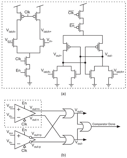
Figure 5.
(a) Comparator schematic of the nFET-based comparator. A complementary pFET-based comparator is also used in parallel. (b) Complete comparator schematic showing both the nFET-based (dashed box) and pFET-based comparators operating together. The MSB selects which version to use to maximize the input range of the complete comparator circuit.
During the first successive approximation, it is already known that one of the comparator inputs will be at the mid-rail voltage because the DAC output will be selected to be midrail by the SAR. Therefore, either a pFET-based or nFET-based comparator would be able to perform the comparison. We chose the nFET-based version to perform the first conversion. The result of this conversion signifies whether the input is in the top-half or bottom-half of the full-scale range. If it is found to be in the top-half, we perform the remaining conversions using the nFET-based comparator. Conversely, if the input is found to be in the bottom-half, the remainder of the conversion is performed using the pFET-based comparator. The appropriate comparator is chosen by the MSB of the SAR (shown as En in Figure 5), thus ensuring that the comparator never operates in a region where it cannot make an accurate comparison. By intelligently selecting which comparator is used, we are able to convert values along the entire full-scale range.
Our clocked comparator is designed to use negligible static energy by breaking the connection between and ground when the clock is low, and also very little dynamic energy by utilizing minimally sized transistors. Prior to comparison, the clock signal is low, which precharges the nodes. When the clock signal goes high, the nodes are discharged at rates proportional to the voltages at and . These nodes control the subsequent voltage latch stage. The end result is that the output node that corresponds to the higher input voltage will be pulled high. Figure 5b shows the interaction of the nFET- and pFET-based comparators. Their outputs are combined through logic OR gates to provide the final output as well as to create a comparator done signal that serves as the clock signal for the subsequent SAR block.
The drawback to using two symmetric comparators is that two different input-referred offsets must be accounted for in postprocessing. For this implementation, no layout matching techniques were used to address this unequal offset, but it would be a viable technique for helping to mitigate the issue. Another method would be to use programmable floating-gate devices in place of the input pairs. The floating gates could then be programmed with the appropriate charge so that the offsets between the two halves of the comparator are matched [20]. Alternately, by using floating-gate transistors as the input transistors, the comparator could be reduced to a single, non-symmetric version (i.e., as shown in Figure 5a) by programming the common-mode charge of the two floating-gate transistors to remove offset as well as to cover rail-to-rail input voltages.
3.2.3. Time-to-Digital Converter
The intersample times are recorded using a time-to-digital converter (TDC). A TDC is simply a device that takes some periodic signal and uses it to estimate the time interval between signal pulses [21]. Our TDC implementation, which is shown in Figure 6, was designed to take a small amount of physical area and digital support circuitry. The periodic signal is created by current-starved inverters arranged in a voltage-controlled oscillator topology. The current starving inverter, which is shown in Figure 7a, ensures that we can both mitigate the power wasted by short-circuit current and that we can control the frequency of oscillation of the overall device. The voltage bias is held at a DC value and the output oscillations are recorded using a digital counter. The output of this counter is then a binary word that is proportional to the length of time since the last restart pulse. The restart/event pulse is provided by the RAMP system and is used to reset the counter values to zero when a new sample is detected. The current version of this system does not account for overflow conditions of the counter, but future iterations would trigger a conversion by the ADC when the TDC reaches a state of all ones in order to maintain accurate representation of very-low-frequency signals.
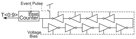
Figure 6.
Time-to-digital converter consisting of a voltage-controlled oscillator and a counter. The counter keeps track of the number of oscillations. The event pulse clears the counter and also shorts part of the oscillator to logic high, which ensures that it begins in the same state after every reset.
Figure 7.
(a) A simple delay unit using a current-starved inverter. The delay is proportional to the size of the capacitor and inversely proportional to the current flowing through the inverter. (b) A simple binary counter. The D flip-flops are sequentially linked and output successive binary numbers.
4. Asynchronous Sampling Implementation
4.1. Extrema Sampling
The first task in implementing this system is to determine what signal quality will serve as the ‘trigger’ for conversion. In conventional data-conversion systems, a fixed sampling rate that is greater than the Nyquist sampling rate is used to acquire the samples—therefore, the system clock is the only external trigger needed for acquiring new sample values for conventional ADCs. On the other hand, asynchronous sampling methods adapt the sampling rate to the changing frequency content of the signal, so triggers within the signal itself must be used to determine when to take a new sample.
The RAMP device could be used to implement a variety circuits capable of finding triggers embedded within the signal that can be used to initiate conversion. We have chosen to focus on the detection of local extrema (i.e., local maxima and minima) to implement an ‘extrema sampling’ system [9,22]. In extrema sampling, the local minimum/maximum voltages are converted when the first derivative of the input is zero. Because the sampling is asynchronous, the time between each sample must also be recorded.
It is also worth reiterating that adaptive-sampling techniques, such as extrema sampling, are a good opportunity for power savings in converting ‘bursty’ signals—ones that have short segments of high-frequency events followed by large segments of relative inactivity. No energy is wasted on digitizing the input signal if it is not changing.
Figure 8 illustrates the reduction in the number of samples that can be obtained over traditional fixed-rate sampling techniques. The highest-frequency spectral component defines the Nyquist sampling rate for fixed-rate sampling systems—for this example waveform, 27 samples would be required over this time period when sampling at the Nyquist rate. In extrema sampling, only the local maxima and minima are sampled. In this way, extrema sampling adapts itself to the changing frequency content of a signal. When applied to this example waveform, only 9 sample values are required to accurately represent the same waveform. The reduction in the number of sampling points when using extrema sampling becomes more pronounced during periods of inactivity and/or only low-frequency content. As a result, significant energy can be saved through the conversion process, and superfluous data points are never converted.
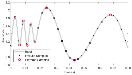
Figure 8.
Comparison of constant-rate Nyquist sampling versus an adaptive-sampling method using extrema sampling.
The original signal can be reconstructed from the extrema samples by employing a simple method used for constructing complex lines in computer graphics called Bézier curves [23]. The Bézier curve is a cubic polynomial capable of providing a smooth curve between two points when given well-defined inflection points. The cubic formula has four parameters: Two end points ( at x = 0 and at x = 1) and two concavity points ( and ). The Bézier polynomial is given by the following expression:
We use this formula as a point-to-point operation between every pair of adjacent extrema. In doing so, N extrema samples are used to create N-1 segments that approximate the complete signal. For each N-1 segment, Equation (1) must be applied to the voltages (V) and times (T) of the samples separately. Figure 9a illustrates how Equation (1) is applied to create a smooth interpolation between extrema values, and, in this particular example, the waveform goes from a local maximum to a local minimum. We let and be represented by the voltage–time pairs of the two extrema locations, given by = (, ) and = (, ).
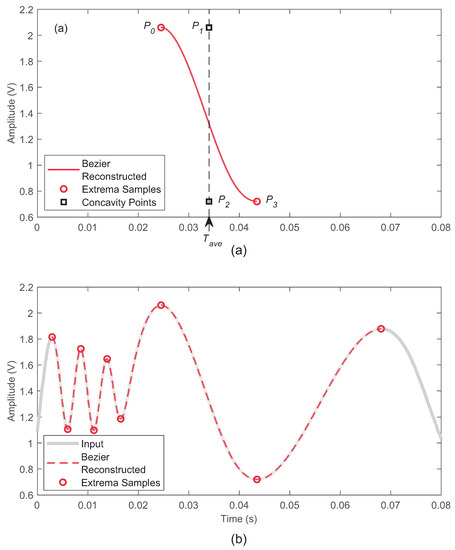
Figure 9.
(a) A Bézier interpolated segment constructed via endpoints and with concavity points and defining the directional path. is the center point between endpoints and . (b) A continuous piecewise Bézier reconstruction that was generated from local maxima/minima and overlaid on the input signal.
Concavity points and define the smooth transition between the endpoints. They maintain the corresponding voltage values of the endpoints (i.e., and ) to ensure that the derivative at the local maxima/minima is zero, but their time values are set exactly halfway between them in time at = . Accordingly, Equation (1) is modified to two equations for the voltage and time expressions.
These expressions create vectors of voltage and time values, providing a smooth curve that is nearly sinusoidal in nature between the two extrema locations.
This process is demonstrated in Figure 9b, which shows a composite Bézier-reconstructed signal created in a piecewise fashion following the pattern of a maximum to a minimum to a maximum to the remaining extrema. We have found that the utilization of the Bézier equation is an apt method for reconstructing a signal using local extrema values, and what we have shown here is the simplest application of it. In Section 5, we demonstrate that this technique can reconstruct complex waveforms with very small mean-squared error between the original waveform and the reconstructed version.
4.2. RAMP Triggering Implementation
Using the reconfigurability available from the RAMP system, we are able to synthesize a circuit capable of locating and sampling extrema values. Figure 10 shows the circuit we synthesized for finding local maxima; the local minima detector circuit is a symmetrically equivalent circuit (not shown). Figure 11 shows the measured output of the maxima and minima detectors that were synthesized on the RAMP, along with timing diagrams showing the outputs of the various stages of these circuits.
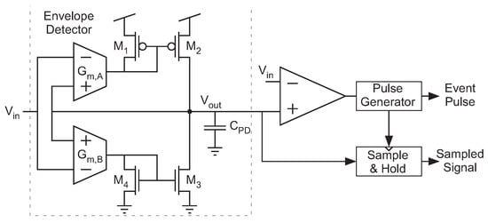
Figure 10.
The maxima detector circuit, which makes up one half of the analog front-end synthesized in the RAMP system. The minima detector circuit is the symmetric equivalent.
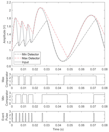
Figure 11.
The maxima and minima locator circuits find local extrema by comparing the output of an envelope detector with the input signal. The measured timing diagrams indicate when an event (local maximum/minimum) has been detected.
Operation of the maxima detector circuit is as follows. Locating the maximum extrema of the signal is performed by first taking the envelope of the signal. This envelope is set to track the input aggressively on the rising edges and to lag behind when the signal begins to decline. Accordingly, the transconductance is set to be larger than to achieve this asymmetry in tracking the input signal that results in envelope detection. The comparator then produces a logic high signal when the envelope lags behind the input—signaling a local maximum. This logic high value is used to trigger a pulse generator which provides the ‘event pulse’ signal shown in the bottom plot of the Figure 11.
An event pulse is triggered to logic high at every extrema occurrence and corresponds to the start pulse signals in Figure 1 and Figure 3. This signal commences the digitization process in the ADC and TDC and also activates the sample-and-hold to sample the value of the signal. The ADC takes the sampled value from the sample-and-hold circuit and converts the voltage into its corresponding digital codeword. The TDC utilizes the event pulse to halt its operation, allowing readout of the digital codeword representing the time duration since the previous extrema occurrence. The TDC is then reset, allowing it to begin counting up until the next extrema occurrence.
5. System Implementation and Example Applications
In this Section, we present the complete fabricated system and its application to three biorelated application examples including voice, electromyography (EMG), and electrocardiogram (ECG).
The designs presented for these applications were measured from fabricated chips. The RAMP was fabricated in a standard 0.35 m CMOS process, while the ADC/TDC was fabricated in a 0.5 m CMOS process. Both die photographs are shown in Figure 12. Future implementations would combine both the RAMP and the asynchronous ADC/TDC on the same die to improve overall performance. Additionally, scaling the ADC down to a newer technology node would also significantly improve power consumption, particularly since the SA-ADC and TDC are mainly comprised of digital circuits.
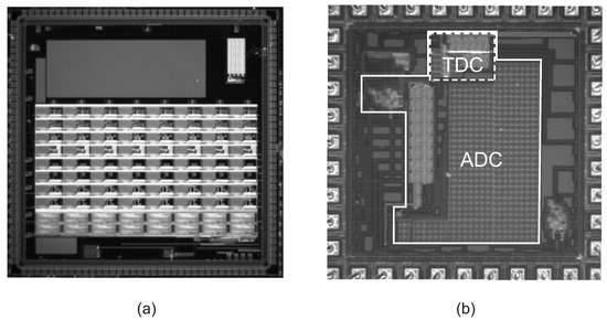
Figure 12.
(a) Die photograph of the reconfigurable analog/mixed-signal platform (RAMP) fabricated in a 0.35 m standard CMOS process. (b) Die photograph of the asynchronous ADC/TDC fabricated in a 0.5 m standard CMOS process.
5.1. Power Consumption
In general, the RAMP power consumption is dependent upon the circuit that is synthesized for the front-end application. In the examples of this Section, the signals can be characterized as biorelated signals with low frequency components (i.e., kHz). By performing this extrema location preprocessing in the analog domain for these biorelated signals, we were able to detect extrema at a measured static power consumption of 4.95 W [1].
The ADC has an extremely low static current draw, measured with an overall static power consumption of 14.75 nW. The low static power consumption means that the ADC can remain powered on between samples without worry of draining the power budget. Energy per conversion was too low to be measured experimentally, so the energy per conversion was obtained from simulation as 47.4 nJ.
The TDC can operate with frequencies ranging up to tens of kilohertz, but, for the example applications shown here, the TDC was operated at a frequency of 1.15 kHz with a measured power consumption of 1.01 W. It should be noted that this component will greatly benefit from smaller CMOS technology nodes and lower power supplies.
A summary of the performance of the fabricated RAMP, SA-ADC, and TDC is provided in Table 1.

Table 1.
Summary of ADC and TDC specifications.
5.2. Voice Recording
The first application demonstrated is the capture and quantization of extrema values within a speech recording. Low-power speech sampling and reconstruction is useful in IoT devices which actively listen for predefined commands. In these applications, perfect reconstruction is not necessary. Instead, only a certain mean-squared error threshold must be respected so the system can identify known commands.
Figure 13 shows the successful capture of 1436 extrema values in a 1.45 s speech waveform. The fastest captured component of the signal is 5333 Hz, thus dictating a minimum of 15,528 samples to be taken in a traditional Nyquist-rate sampling system. Extrema sampling results in a nearly eleven-times reduction in sample values and maintains a 0.0483 mean-squared error rate when reconstructed using the Bézier interpolation technique of Section 4.
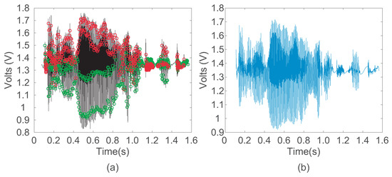
Figure 13.
(a) The original vocal waveform with successfully detected peaks. (b) The recreated vocal waveform using Bézier reconstruction.Results of a vocal signal extrema capture and quantization
The reduced number of samples provided by the asynchronous sampling can significantly reduce the overall power consumption of the system, both at the conversion stage and at the subsequent digital processing stage when the data are analyzed. To provide a comparison in the power consumption of only the data-conversion stage, we can use the power and energy values provided in Table 1 to determine the power savings of the asynchronous ADC over an identical ADC continuously converting all data at a fixed rate. The average power consumption of the data converter is given by
where the P values are the static power consumption of the associated stages (with for a fixed-rate converter), n is the number of samples taken over a time interval (t), and is the energy required by the ADC to convert one sample. As a simplification, we let also represent the power consumed by a fixed-rate clock for a traditional ADC. Note, however, that a fixed-rate ADC would need a faster clock than the asynchronous case, thereby meaning that the fixed-rate ADC would likely consume even more power.
Based upon the values in Table 1 and Equation (4), our asynchronous converter would consume an average of 52.9 W, while a fixed-rate ADC (without any analog preprocessing) would consume an average of 509 W for this voice-recording application. As a result, the asynchronous ADC consumes 9.6-times less power than a fixed-rate converter. While these specific numbers depend on the exact characteristics of the ADC that is used, the fundamental principle holds that reducing the number of samples that are converted can significantly decrease the overall power consumed by an ADC, as is clearly seen by the last term in Equation (4). As a result, using even-more power-efficient ADCs along with analog preprocessing would result in even further savings. Furthermore, in this voice-recording example, the speech is continuous throughout the 1.45 s waveform. For many real-world applications, pauses in the speech would be present, which would further reduce the power consumed by the asynchronous ADC, but not the fixed-rate ADC.
5.3. Electromyography
The next application involves the quantization of an electromyography (EMG) signal. EMG signals are traditionally used to diagnose muscle and nerve health. In addition to measuring neuro-muscular health, EMGs are gaining popularity in measuring muscular exertion in physical therapy and sport-science applications [24]. As these applications become more advanced, increasingly power- and sample-efficient devices will be required.
Figure 14 demonstrates the results of our presented system on an EMG waveform taken from the example EMG database found at [25]. Over the 12.7 s signal, 3035 extrema values were successfully detected. Given that the highest frequency within the sample was approximately 2 kHz, then 50,796 samples would be required for an equivalent Nyquist-rate sampling system. Therefore, our extrema sampling quantizer represents a greater than 16-times sample reduction over standard techniques, while maintaining a mean-squared error in reconstruction (using Bézier reconstruction) of less than 0.0036. Applying Equation (4), the asynchronous ADC has a factor of 11-times less average power consumed than the fixed-rate ADC for this EMG example.
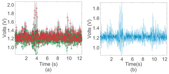
Figure 14.
(a) The original electromyography (EMG) waveform with successfully detected peaks. (b) The recreated EMG waveform using Bézier reconstruction.Results of an EMG extrema capture and quantization
5.4. Electrocardiogram
Finally, we present an application where the goal is not reconstruction, but instead the capture of specific points of data. Electrocardiogram (ECG) waveforms are very well understood signals that have a limited number of medically relevant data points. Our example will focus on QRS-complex capture, disregarding the other portions of the ECG wave. QRS-complexes are useful for a variety of medical purposes, ranging from monitoring for hyperkalemia or cardiac hypertrophy to simply extracting heart-beat to estimate perceived exertion [26]. For the purpose of demonstrating this system, an extrema sampling approach is a natural fit for reducing an ECG waveform to its QRS-complex—which can be viewed as a distinct local maximum between two local minima. By extracting only the QRS-complex and avoiding sampling extraneous data, this device would allow a wearable health or fitness system to be a more viable long-term option.
Figure 15 shows the operation of the system and the resultant approximations of the amplitudes and time intervals between the QRS peaks. The QRS waveform of Figure 15b was not reconstructed using Bézier reconstruction—a simplistic interpolation technique based upon QRS shapes is adequate to glean the medically-relevant information from the QRS-complex for this particular case. The device was tested with real world data taken from the MIT arrhythmia database [25].
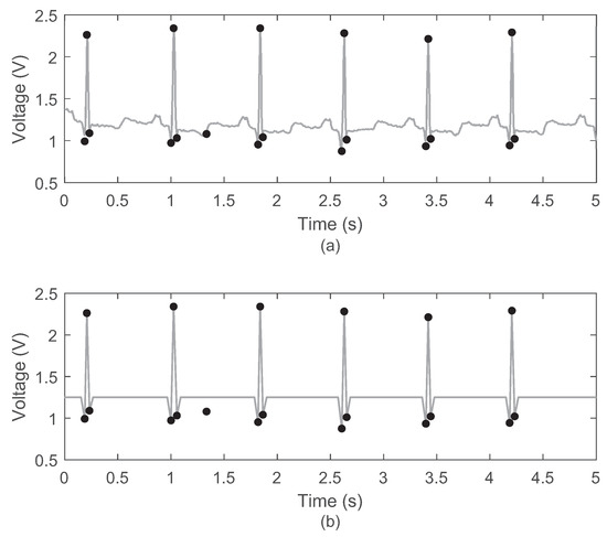
Figure 15.
(a) The original ECG waveform taken from the MIT arrhythmia database with the detected extrema values shown as dots. (b) QRS-complex reconstruction using a simplistic quasi-linear model based on QRS waveform shapes (line) with the detected QRS values (dots) as well as a single false positive.Results of an electrocardiogram (ECG) extrema capture and quantization
Figure 15 shows the system effectively capturing a QRS-complex. The highest frequency component, which is the change between Q and R, would determine the minimum sampling rate in a traditional Nyquist sampling scheme. For the demonstrated waveform, the 57 Hz change would necessitate a sampling rate of 114 Hz from a conventional Nyquist-rate ADC. This sampling rate would yield approximately 485 samples over the 4.228 s that the signal is demonstrated over. That amount of superfluous samples is greater than 25 times the number of samples taken in our system, even including the single false-positive. Since the frequency of sampling is much lower than for the voice and EMG cases, the amount of power savings using Equation (4) is not nearly as significant. However, two points should be noted. First, most ADCs that are designed for heart-rate monitoring use faster sampling rates than the absolute minimum from this example. For example, [27,28,29,30] use sampling rates from 300 Hz to 600 kHz, and using these larger sampling rates would significantly increase the average power consumption in an equivalent ADC. Second, the purpose of many heart-monitoring systems is to determine the features of the QRS complex—while our asynchronous ADC has minimal power savings strictly at the conversion stage for this application, our asynchronous ADC is performing many of the operations that would be reserved for a subsequent digital processing system when using a traditional ADC, which would also have a substantial power consumption. Some application-specific QRS detector systems have been shown to acquire and process heart-rate data at very low power; for example, the system of [30] is able to operate at 220 nW under a 300 mV power supply. However, such a system lacks the flexibility afforded by our reconfigurable analog preprocessing. Additionally, scaling both the technology node and power supply of our ADC (to levels similar to [30]) would also help to significantly further reduce the overall power consumption.
6. Conclusions
To reduce the power consumption of an analog-to-digital conversion system, we have introduced an analog preprocessing stage prior to an asynchronous converter to find the data values that are most important to be converted for a given application. Since the timing of the data values is not known a priori, the analog preprocessing triggers the asynchronous converter to acquire a sample, and a time-to-digital converter measures the intersample time period. By converting only the data values that are needed, a significant amount of power can be saved by the system, both at the conversion stage, as well as further down the signal-processing and/or transmission chain. We also demonstrated a sampling technique based upon finding local maxima/minima, and a variety of other triggering operations are also possible due to the reconfigurable nature of the analog front-end.
Author Contributions
All three authors were responsible for writing this paper. B.M.K. and D.W.G. were responsible for the design of the circuits. B.M.K. and A.T.D. were responsible for all of the experimental measurements.
Funding
This research was funded by the National Science Foundation under Award No. 1148815.
Acknowledgments
This material is based upon work supported by the National Science Foundation under Award No. 1148815.
Conflicts of Interest
The funding sponsors had no role in the design of the study; in the collection, analyses, or interpretation of data; in the writing of the manuscript; and in the decision to publish the results.
References
- Rumberg, B.; Graham, D.; Clites, S.; Kelly, B.; Navidi, M.; Dilello, A.; Kulathumani, V. RAMP: Accelerating wireless sensor hardware design with a reconfigurable analog/mixed-signal platform. In Proceedings of the ACM/IEEE Conference on Information Processing in Sensor Networks, Seattle, WA, USA, 13–16 April 2015; pp. 47–58. [Google Scholar]
- Kelly, B.M.; Graham, D.W. An asynchronous ADC with reconfigurable analog pre-processing. In Proceedings of the IEEE International Symposium on Circuits and Systems, Montreal, QC, Canada, 22–25 May 2016; pp. 1062–1065. [Google Scholar]
- Kinget, P.R. Scaling analog circuits into deep nanoscale CMOS: Obstacles and ways to overcome them. In Proceedings of the IEEE Custom Integrated Circuits Conference, San Jose, CA, USA, 28–30 September 2015; pp. 1–8. [Google Scholar]
- Walden, R.H. Analog-to-digital converter survey and analysis. IEEE J. Sel. Areas Commun. 1999, 17, 539–550. [Google Scholar] [CrossRef]
- Texas Instruments. MSP430F15x, MSP430F16x, MSP430F161x Mixed Signal Microcontroller; Texas Instruments: Dallas, TX, USA, 2002. [Google Scholar]
- Kozmin, K.; Johansson, J.; Delsing, J. Level-Crossing ADC Performance Evaluation Toward Ultrasound Application. IEEE Trans. Circuits Syst. I Regul. Pap. 2009, 56, 1708–1719. [Google Scholar] [CrossRef]
- Martínez-Nuevo, P.; Patil, S.; Tsividis, Y. Derivative Level-Crossing Sampling. IEEE Trans. Circuits Syst. II Exp. Briefs 2015, 62, 11–15. [Google Scholar] [CrossRef]
- Trakimas, M.; Sonkusale, S. An Adaptive Resolution Asynchronous ADC Architecture for Data Compression in Energy Constrained Sensing Applications. IEEE Trans. Circuits Syst. I Regul. Pap. 2011, 58, 921–934. [Google Scholar] [CrossRef]
- Greitans, M.; Shavelis, R.; Fesquet, L.; Beyrouthy, T. Combined peak and level-crossing sampling scheme. In Proceedings of the International Conference on Sampling Theory and Applications, Singapore, 2–6 May 2011. [Google Scholar]
- Mark, J.; Todd, T. A Nonuniform Sampling Approach to Data Compression. IEEE Trans. Commun. 1981, 29, 24–32. [Google Scholar] [CrossRef]
- Rumberg, B.; Graham, D.W.; Kulathumani, V.; Fernandez, R. Hibernets: Energy-Efficient Sensor Networks Using Analog Signal Processing. IEEE Trans. Emerg. Sel. Top. Circuits Syst. 2011, 1, 321–334. [Google Scholar] [CrossRef]
- Kelly, B.M.; Rumberg, B.; Graham, D.W.; Kulathumani, V. Reconfigurable analog signal processing for wireless sensor networks. In Proceedings of the IEEE International Midwest Symposium on Circuits and Systems, Columbus, OH, USA, 4–7 August 2013; pp. 221–224. [Google Scholar]
- Sarpeshkar, R. Analog versus digital: Extrapolating from electronics to neurobiology. Neural Comput. 1998, 10, 1601–1638. [Google Scholar] [CrossRef] [PubMed]
- Lee, E.K.F.; Gulak, P.G. A CMOS field-programmable analog array. IEEE J. Solid-State Circuits 1991, 26, 1860–1867. [Google Scholar] [CrossRef]
- Mackensen, E.; Muller, C. Implementation of Reconfigurable Micro-Sensor Interfaces Utilizing FPAAs. In Proceedings of the SENSORS, Irvine, CA, USA, 30 October–3 November 2005; pp. 1064–1067. [Google Scholar]
- George, S.; Kim, S.; Shah, S.; Hasler, J.; Collins, M.; Adil, F.; Wunderlich, R.; Nease, S.; Ramakrishnan, S. A Programmable and Configurable Mixed-Mode FPAA SoC. IEEE Trans. Very Large Scale Integr. Syst. 2016, 24, 2253–2261. [Google Scholar] [CrossRef]
- Rumberg, B.; Graham, D.W. A floating-gate memory cell for continuous-time programming. In Proceedings of the IEEE International Midwest Symposium on Circuits and Systems, Boise, ID, USA, 5–8 August 2012; pp. 214–217. [Google Scholar]
- Jonsson, B. An empirical approach to finding energy efficient ADC architectures. In Proceedings of the International Workshop on ADC Modelling, Testing and Data Converter Analysis and Design, and IEEE ADC Forum, Orvieto, Italy, 30 June–1 July 2011; pp. 1–6. [Google Scholar]
- Schinkel, D.; Mensink, E.; Klumperink, E.; van Tuijl, E.; Nauta, B. A Double-Tail Latch-Type Voltage Sense Amplifier with 18ps Setup+Hold Time. In Proceedings of the IEEE International Solid-State Circuits Conference, San Francisco, CA, USA, 11–15 Febuary 2007; pp. 314–605. [Google Scholar]
- Adil, F.; Serrano, G.; Hasler, P. Offset removal using floating-gate circuits for mixed-signal systems. In Proceedings of the Southwest Symposium on Mixed-Signal Design, Las Vegas, NV, USA, 25–25 Febuary 2003; pp. 190–195. [Google Scholar]
- Roberts, G.; Ali-Bakhshian, M. A Brief Introduction to Time-to-Digital and Digital-to-Time Converters. IEEE Trans. Circuits Syst. II Exp. Briefs 2010, 57, 153–157. [Google Scholar] [CrossRef]
- Kelly, B.; Rumberg, B.; Graham, D. An ultra-low-power analog memory system with an adaptive sampling rate. In Proceedings of the IEEE International Midwest Symposium on Circuits and Systems, Boise, ID, USA, 5–8 August 2012; pp. 302–305. [Google Scholar]
- Farin, G. Curves and Surfaces for CAGD: A Practical Guide; Morgan Kaufmann: Burlington, MA, USA, 2001. [Google Scholar]
- DeLuca, C.J. The Use of Surface Electromyography in Biomechanics. J. Appl. Biomech. 1997, 13, 135–163. [Google Scholar] [CrossRef]
- Goldberger, A.L.; Amaral, L.A.; Glass, L.; Hausdorff, J.M.; Ivanov, P.C.; Mark, R.G.; Mietus, J.E.; Moody, G.B.; Peng, C.K.; Stanley, H.E. PhysioBank, PhysioToolkit, and PhysioNet: Components of a New Research Resource for Complex Physiologic Signals. Circulation 2000, 101, e215–e220. [Google Scholar] [CrossRef] [PubMed]
- Yoo, H.; van Hoof, C. Bio-Medical CMOS ICs; Springer: Berlin/Heidelberg, Germany, 2010. [Google Scholar]
- Ieong, C.I.; Mak, P.I.; Lam, C.P.; Dong, C.; Vai, M.I.; Mak, P.U.; Pun, S.H.; Wan, F.; Martins, R.P. A 0.83 μW QRS Detection Processor Using Quadratic Spline Wavelet Transform for Wireless ECG Acquisition in 0.35 μm CMOS. IEEE Trans. Biomed. Circuits Syst. 2012, 6, 586–595. [Google Scholar] [CrossRef] [PubMed]
- Abdallah, R.A.; Shanbhag, N.R. A 14.5 fJ/cycle/k-gate, 0.33 V ECG processor in 45nm CMOS using statistical error compensation. In Proceedings of the IEEE Custom Integrated Circuits Conference, San Jose, CA, USA, 9–12 September 2012; pp. 1–4. [Google Scholar]
- Wang, H.M.; Lai, Y.L.; Hou, M.C.; Lin, S.H.; Yen, B.S.; Huang, Y.C.; Chou, L.C.; Hsu, S.Y.; Huang, S.C.; Jan, M.Y. A ±6ms-accuracy, 0.68 mm2 and 2.21 μW QRS detection ASIC. In Proceedings of the 2010 IEEE International Symposium on Circuits and Systems, Paris, France, 30 May–2 June 2010; pp. 1372–1375. [Google Scholar]
- Zhang, X.; Lian, Y. A 300 mV 220 nW Event-Driven ADC With Real-Time QRS Detection for Wearable ECG Sensors. IEEE Trans. Biomed. Circuits Syst. 2014, 8, 834–843. [Google Scholar] [CrossRef] [PubMed]


© 2019 by the authors. Licensee MDPI, Basel, Switzerland. This article is an open access article distributed under the terms and conditions of the Creative Commons Attribution (CC BY) license (http://creativecommons.org/licenses/by/4.0/).