Memristor-Based Loop Filter Design for Phase Locked Loop


Abstract
1. Introduction
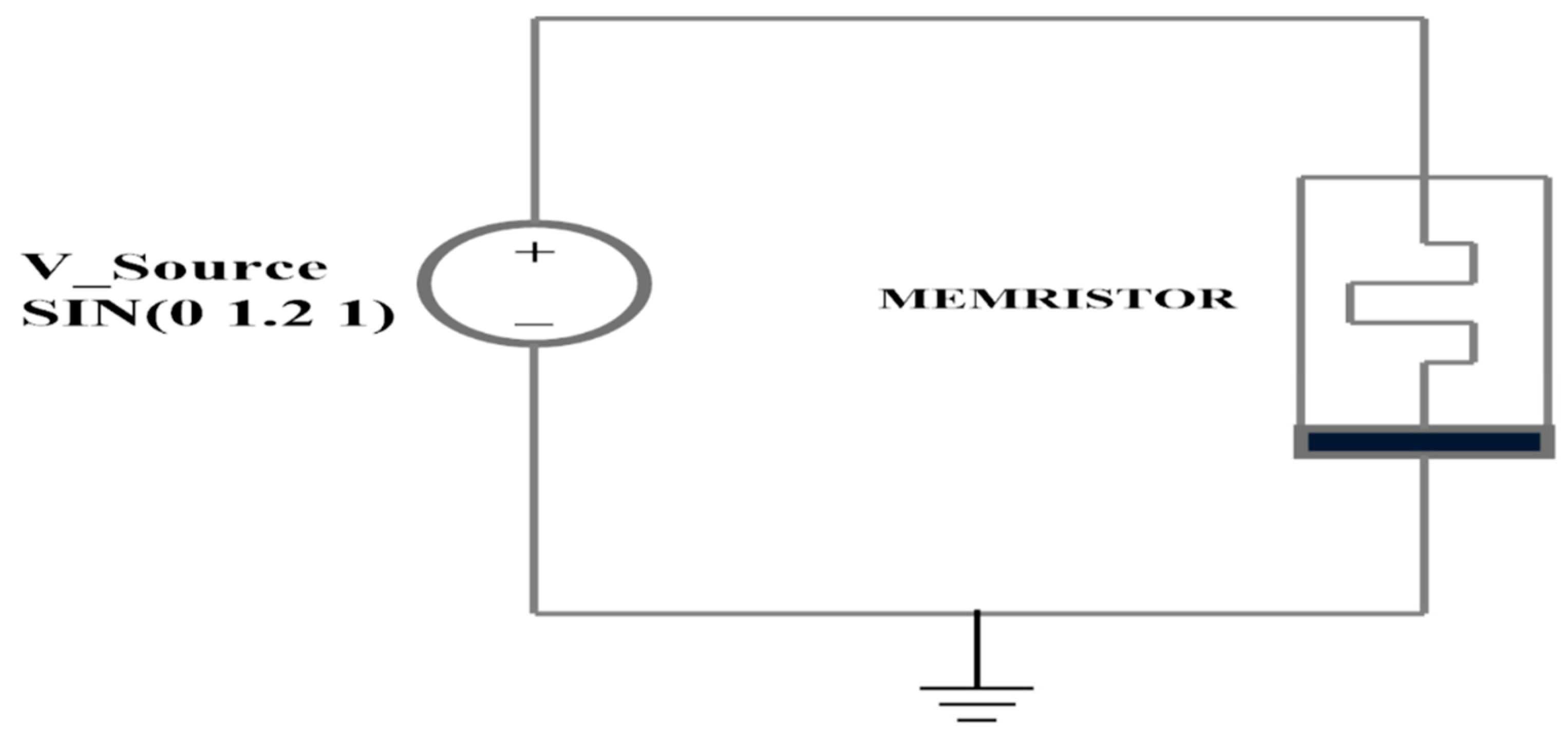
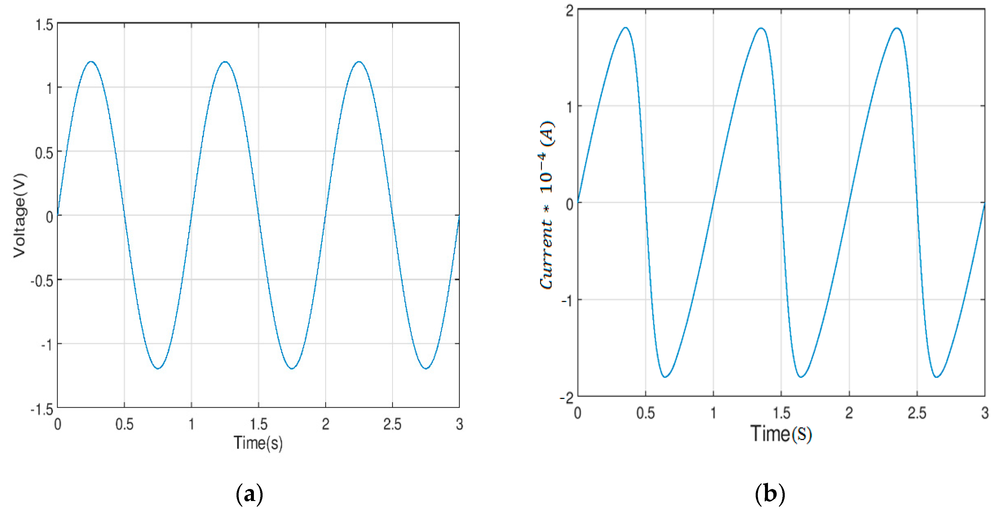
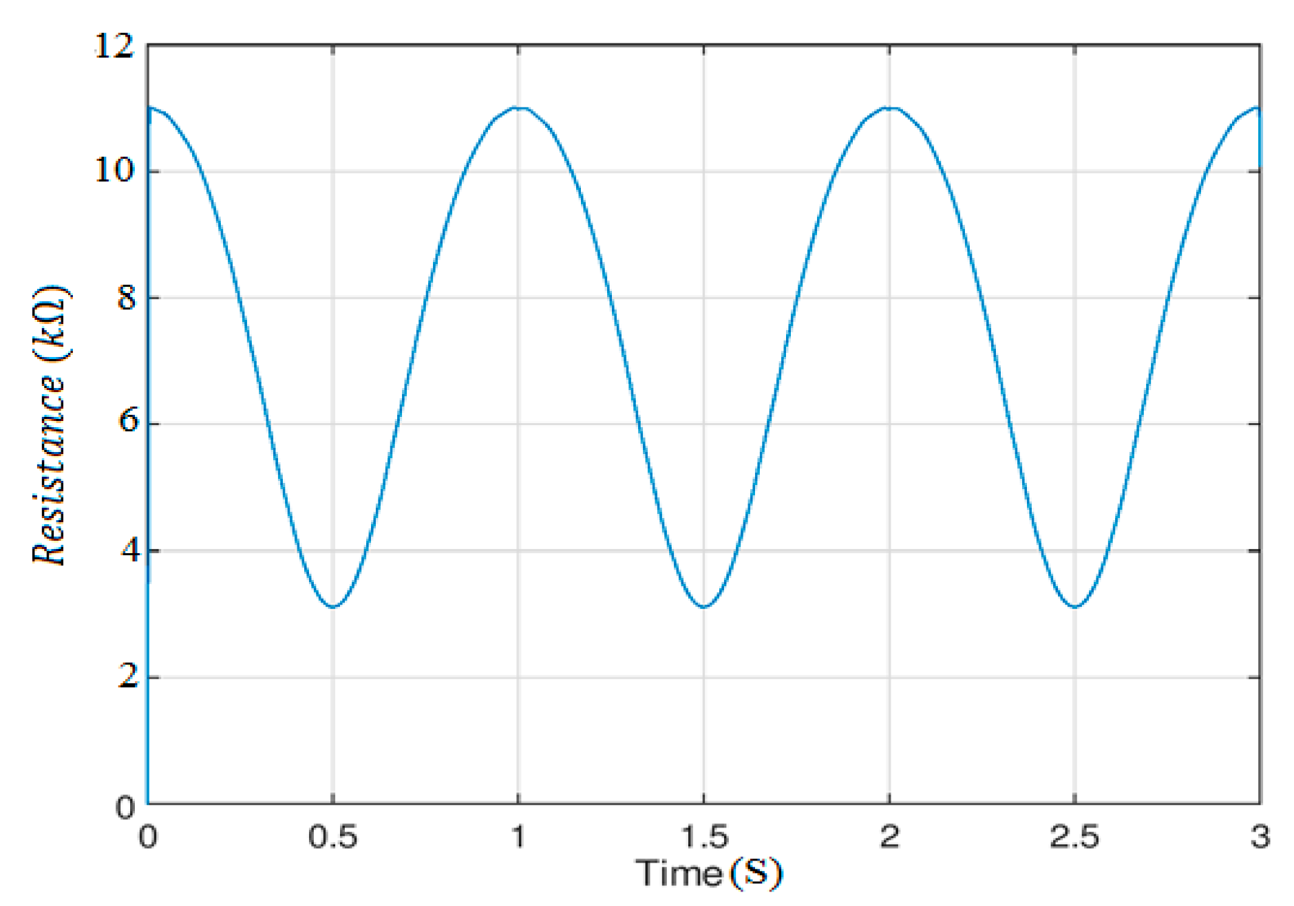
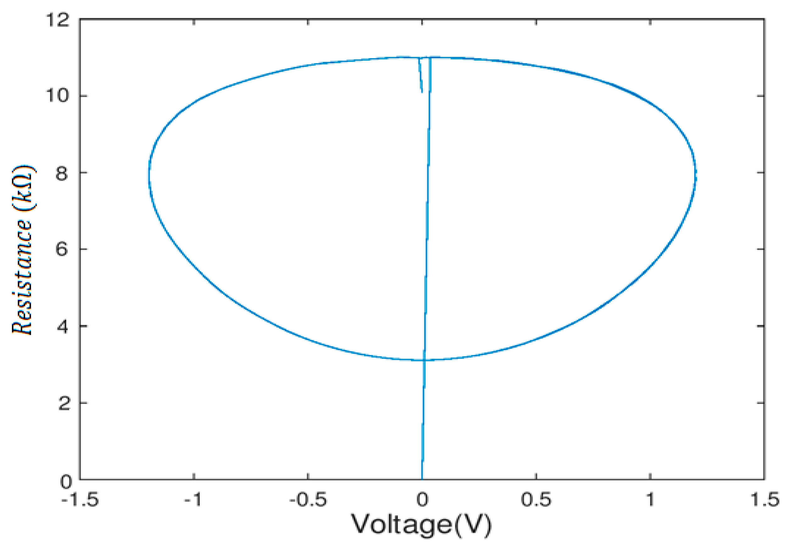
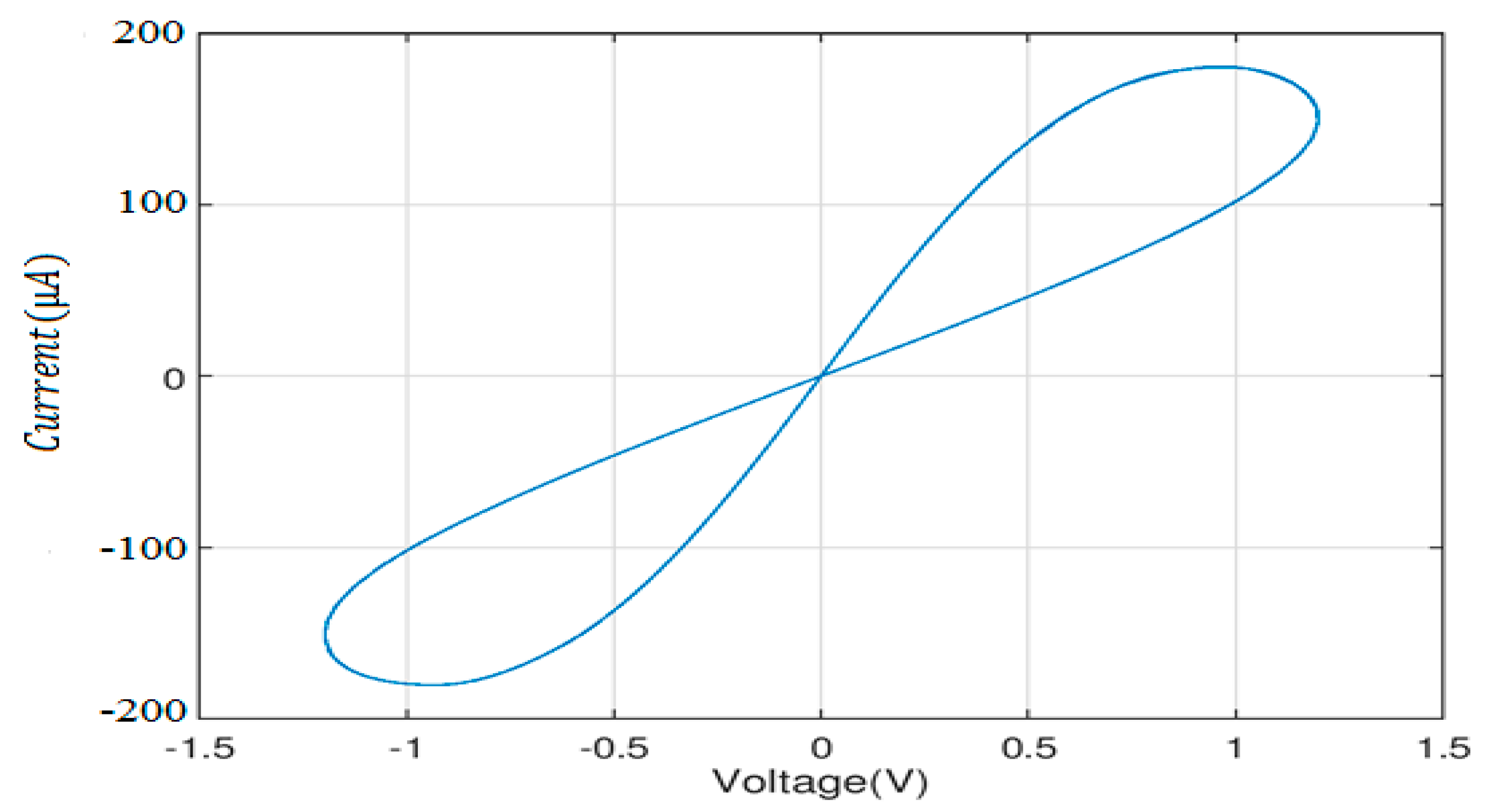
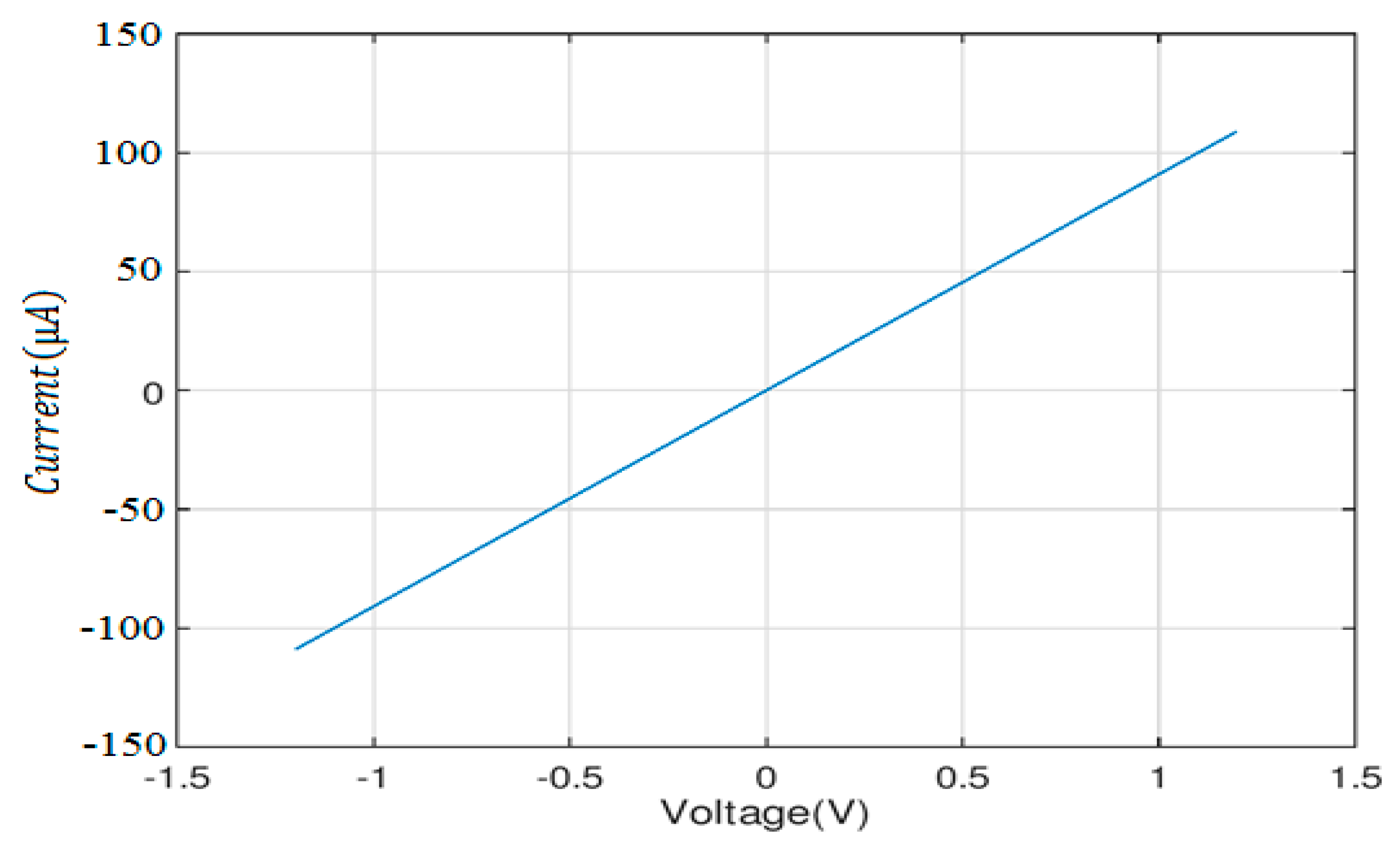
2. Memristor
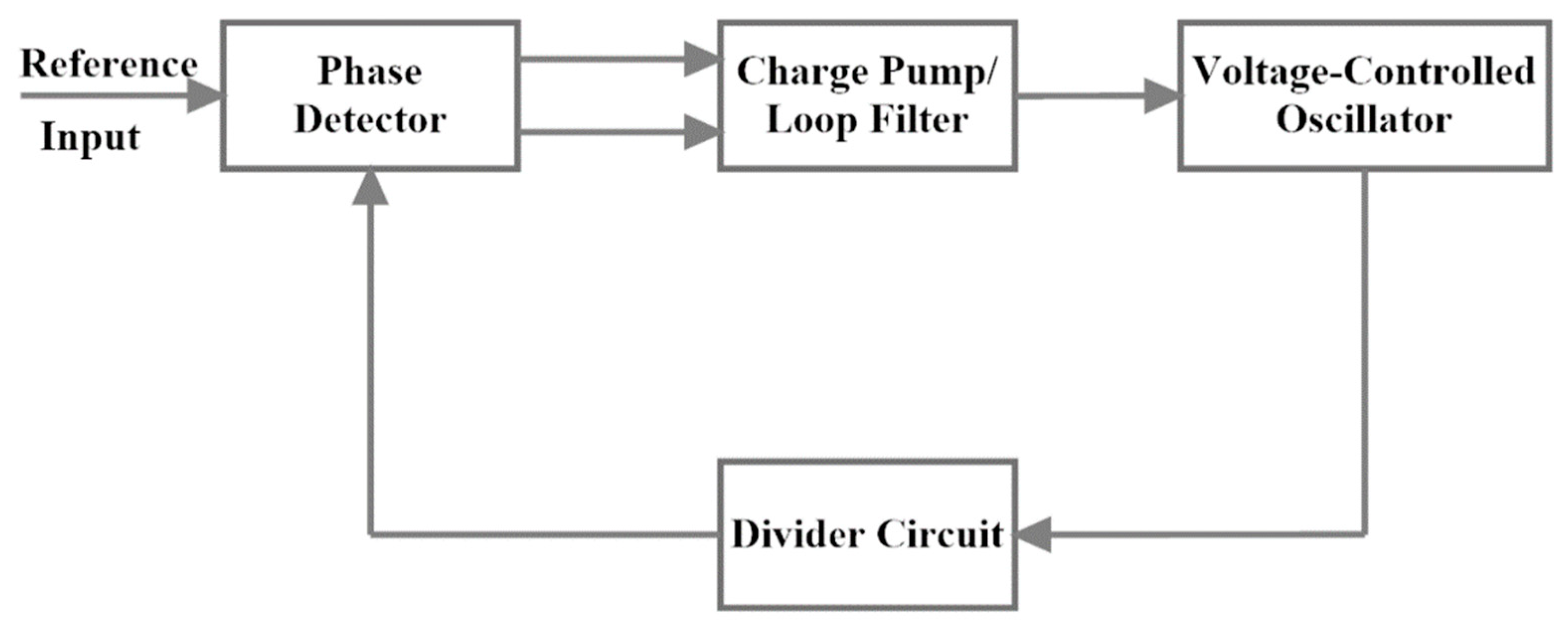
3. PLL Building Blocks
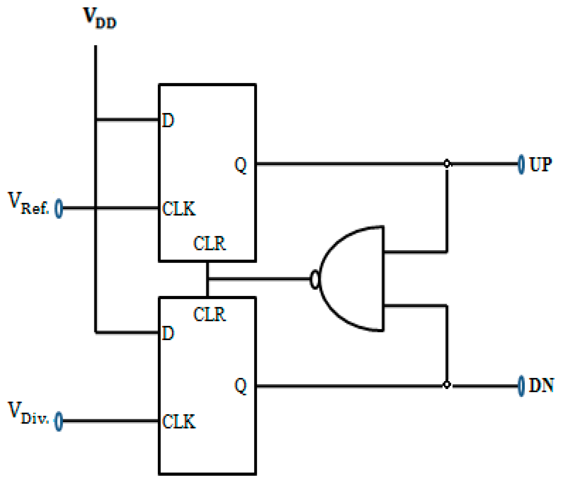
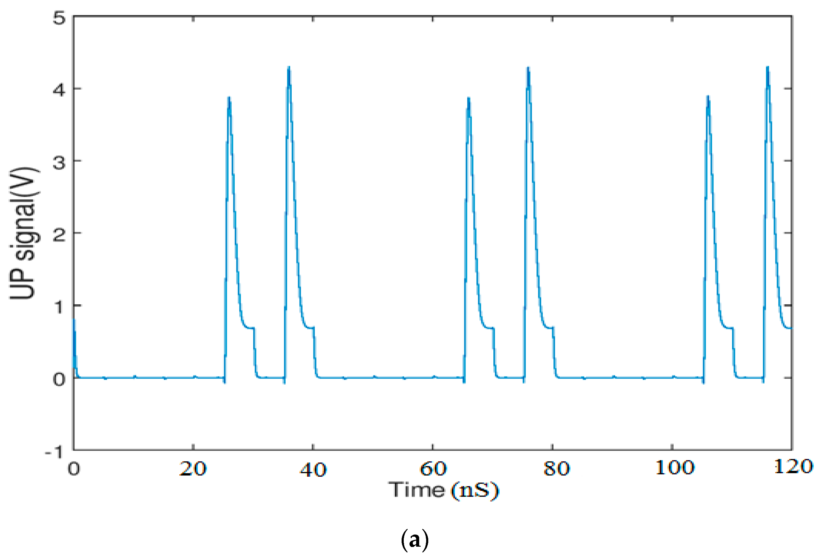
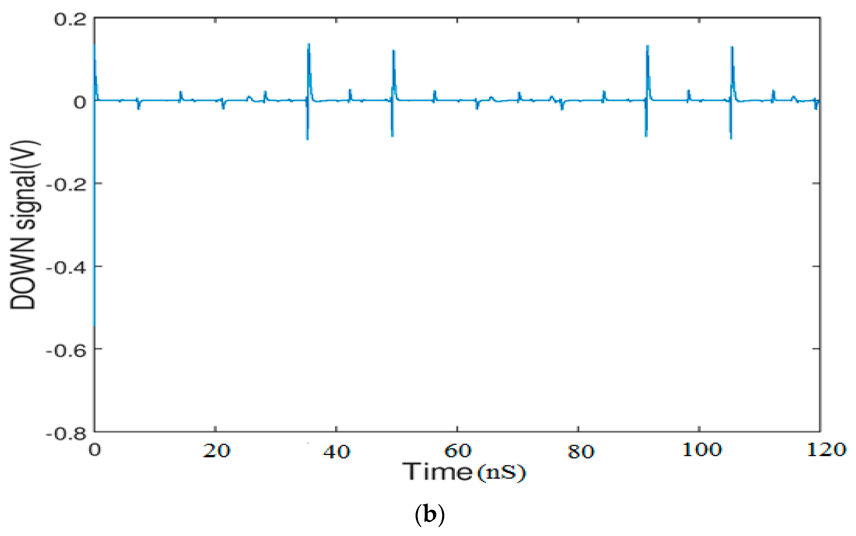
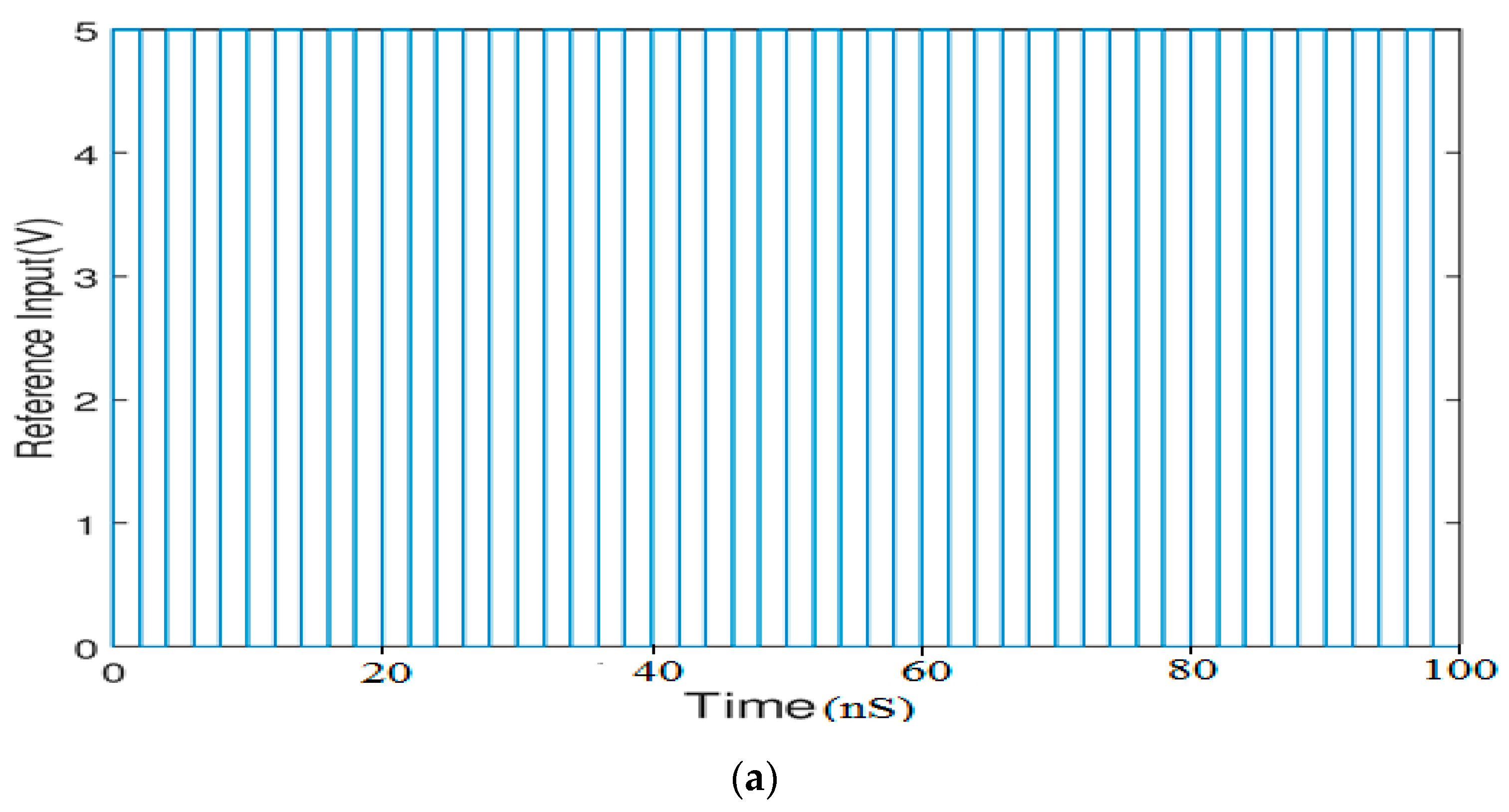
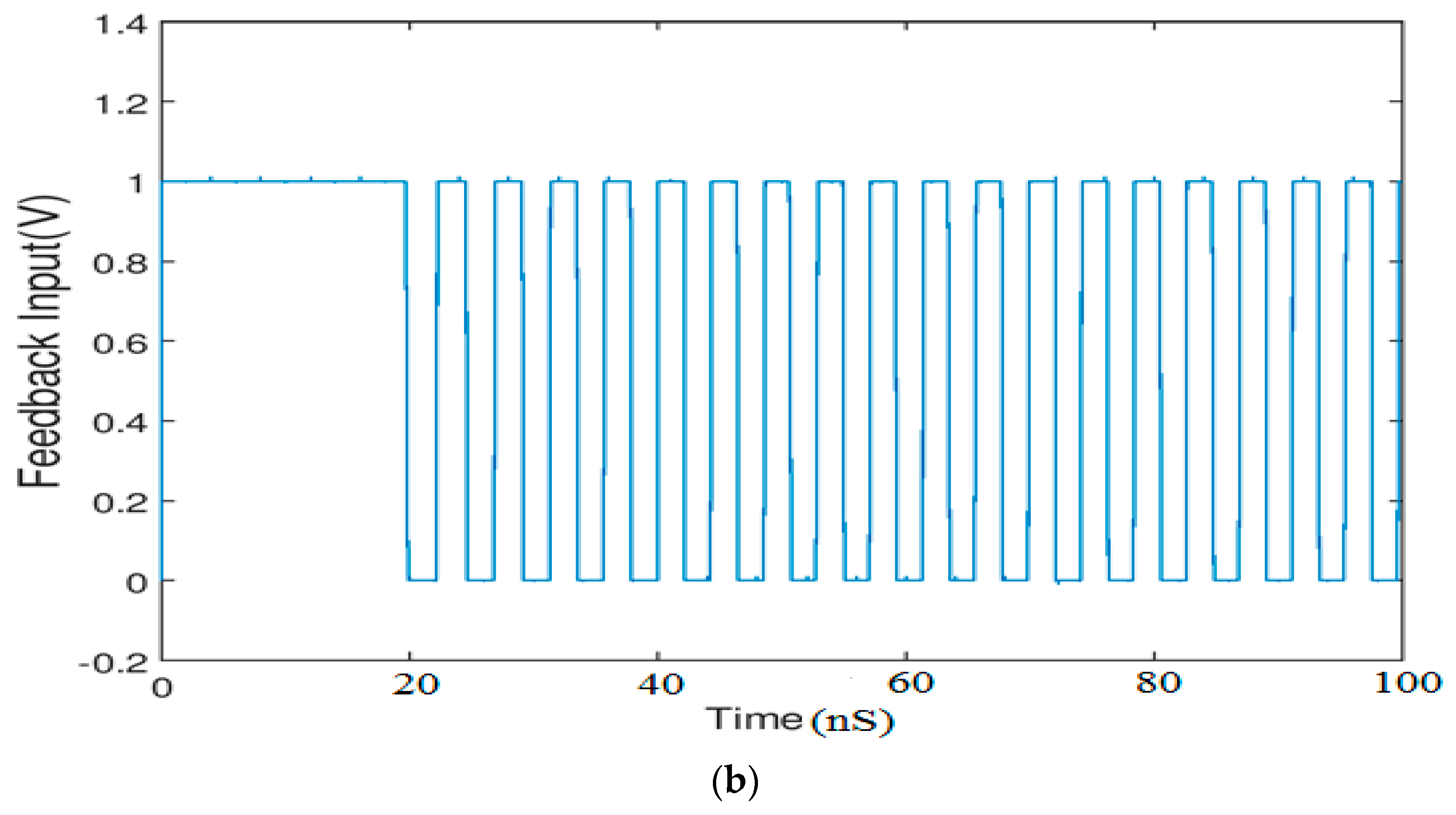
3.1. Phase Detector
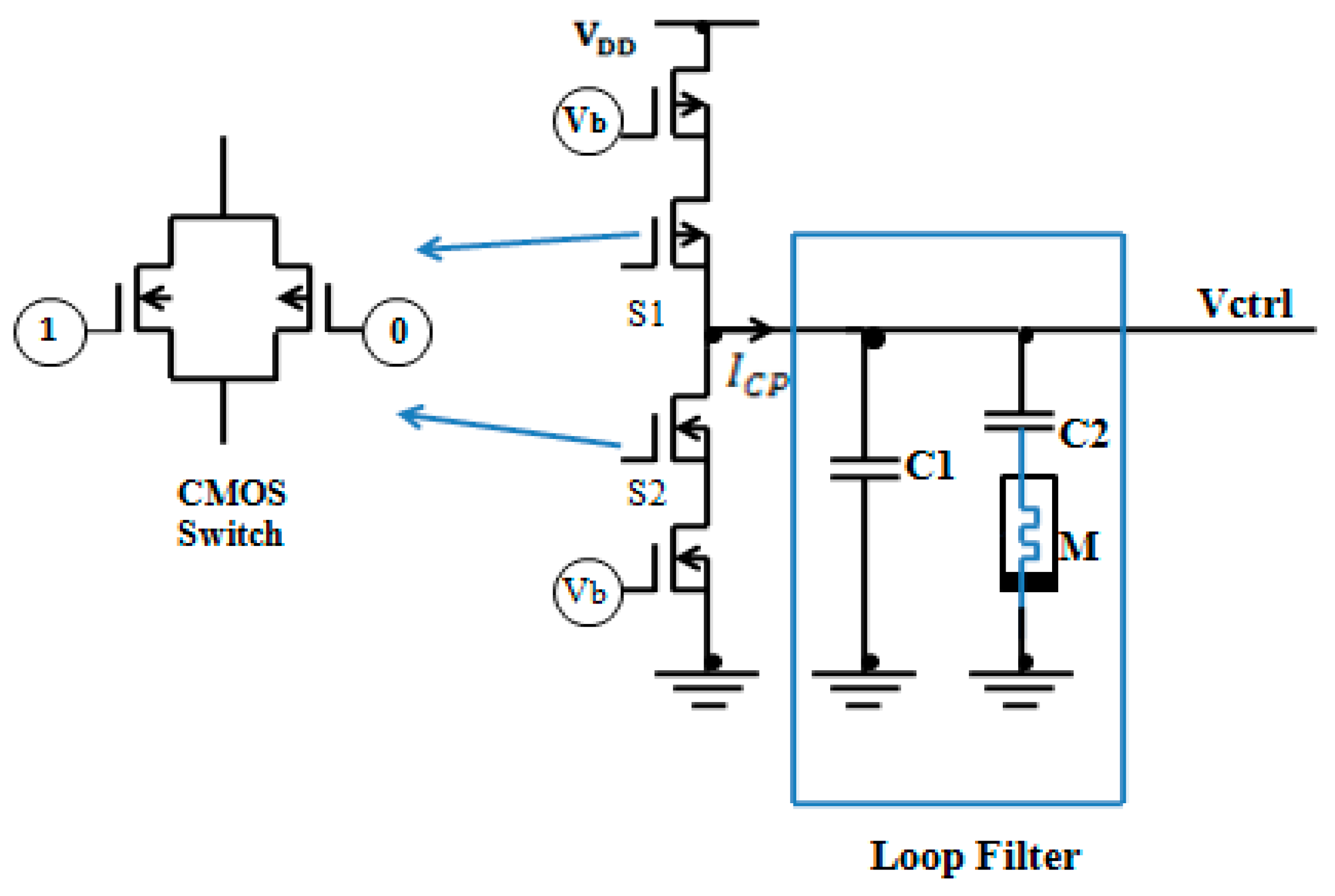
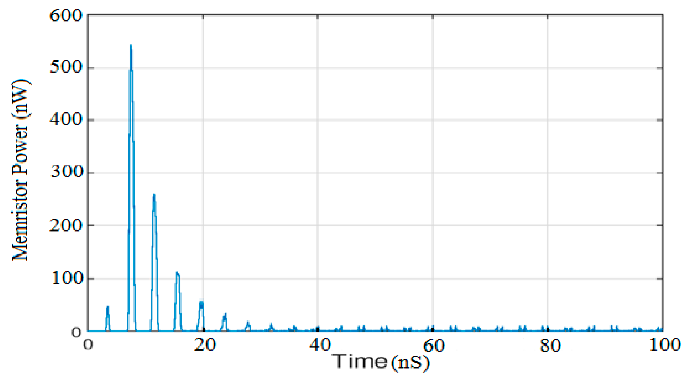
3.2. Charge Pump/Loop Filter
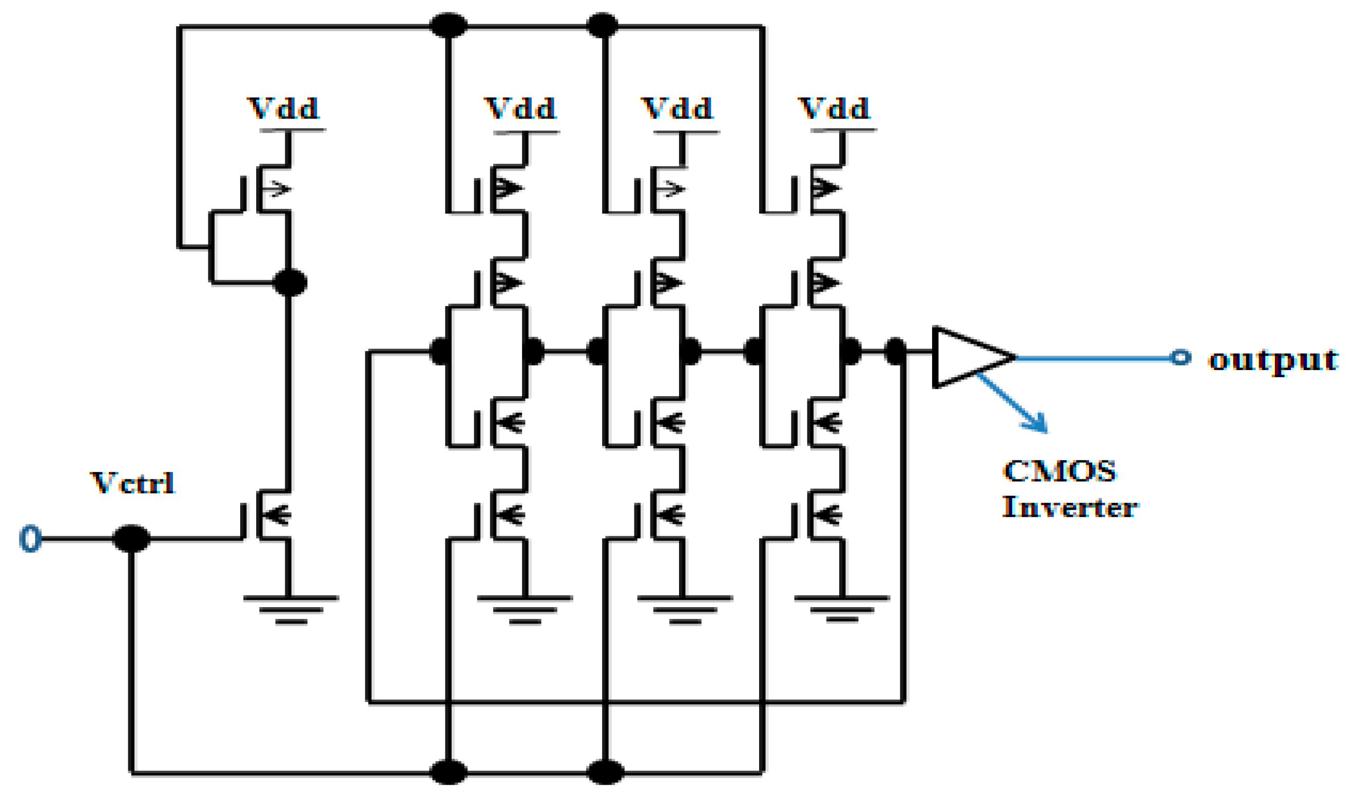
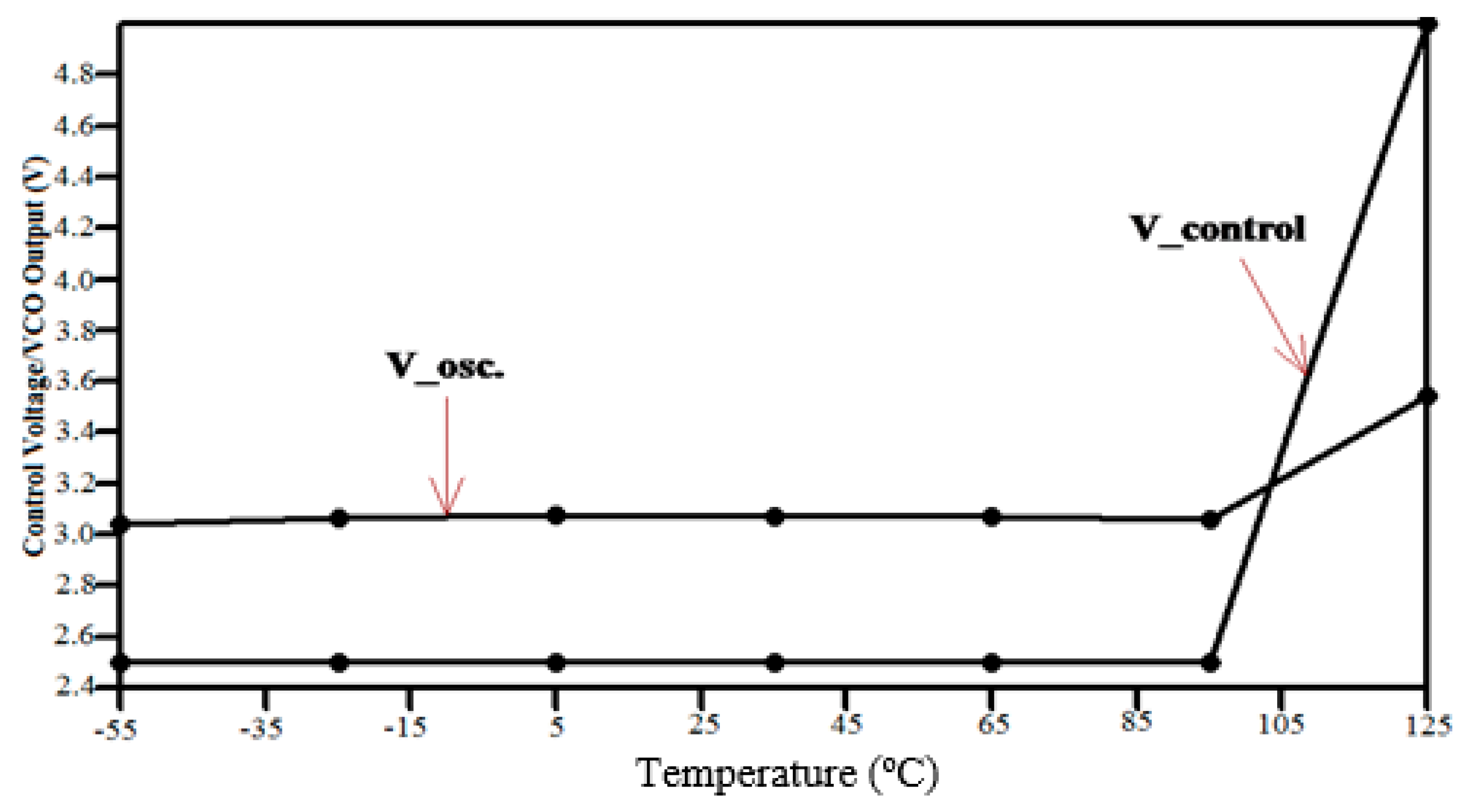
3.3. Voltage Controlled Oscillator
3.4. Frequency Divider
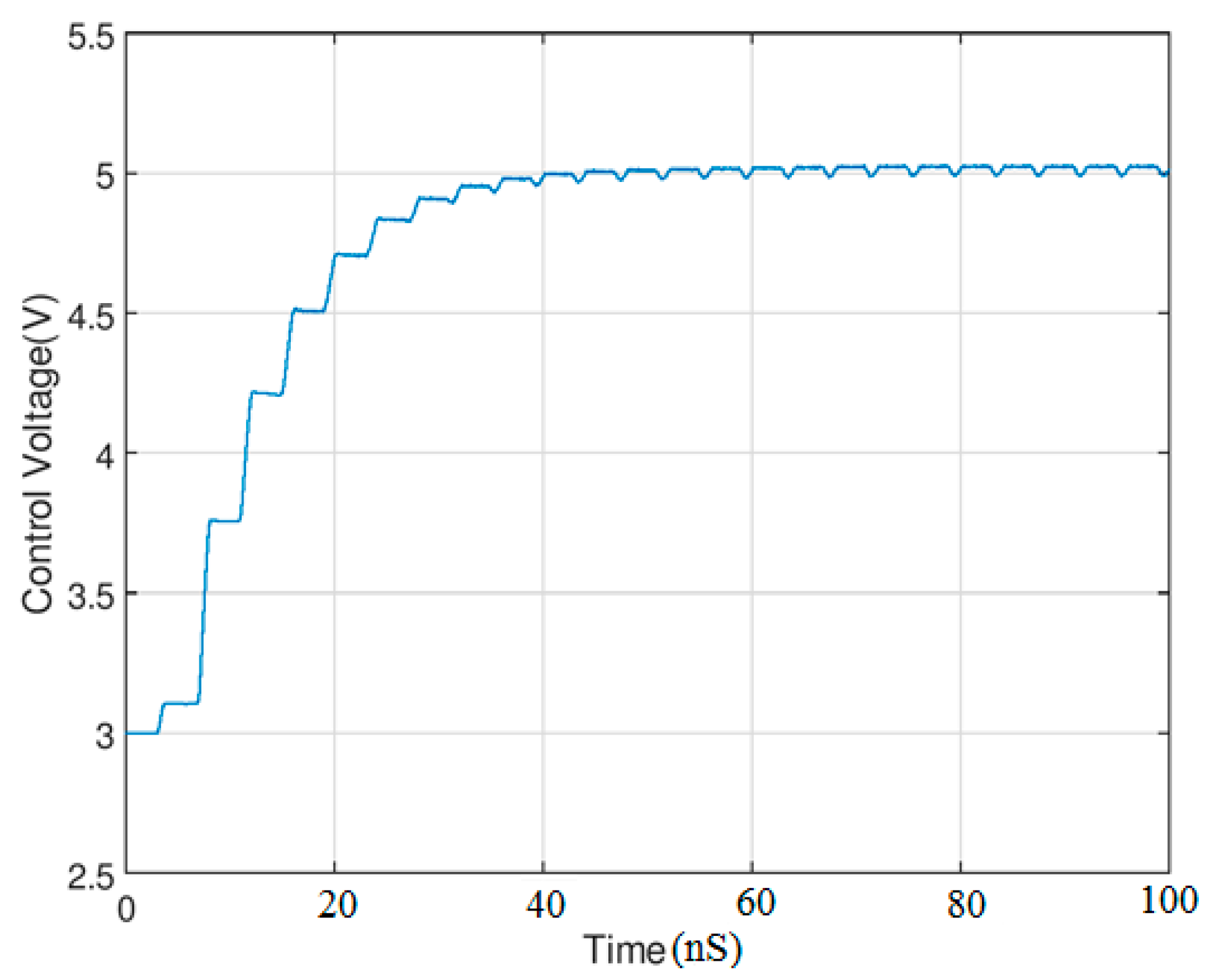
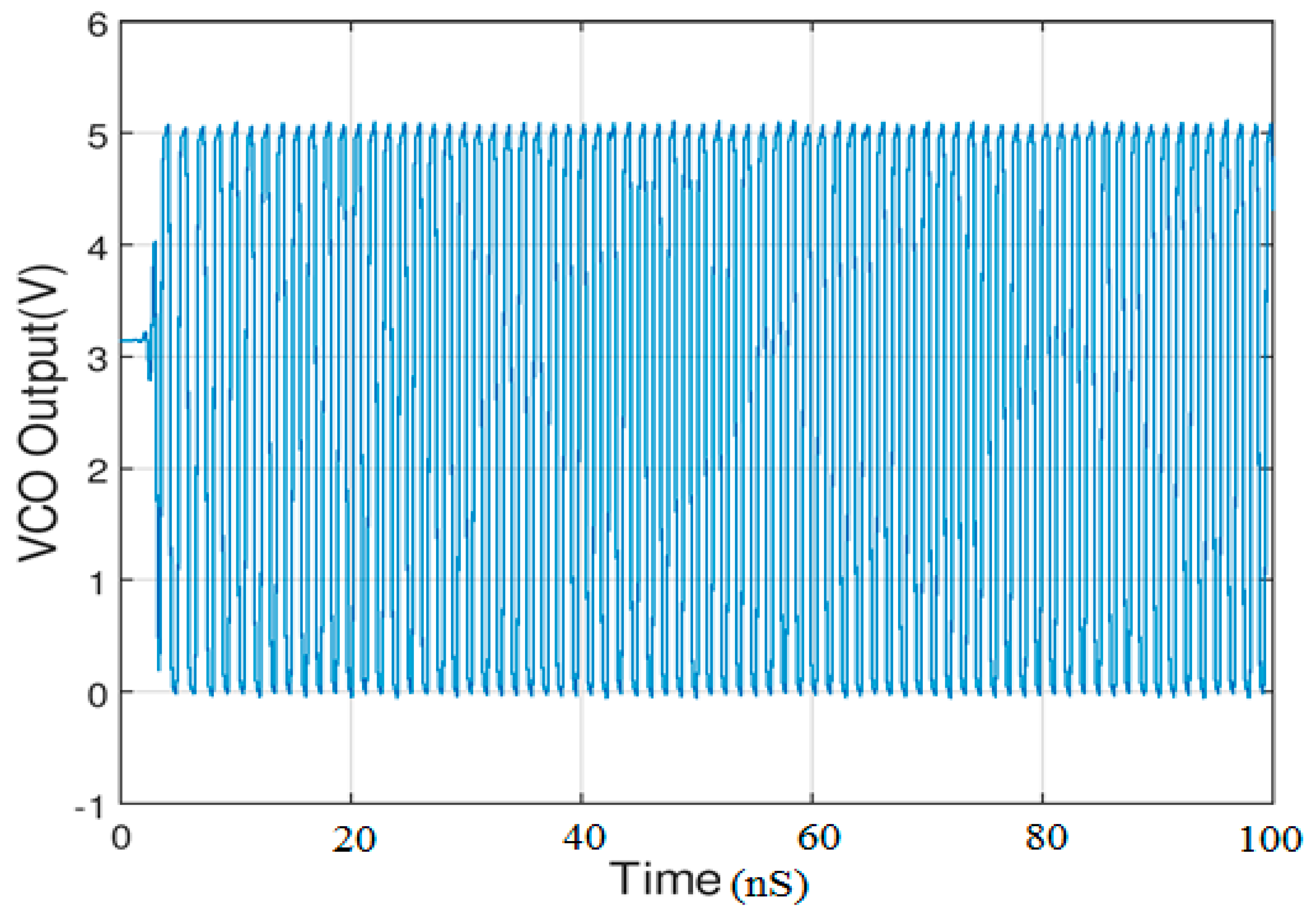
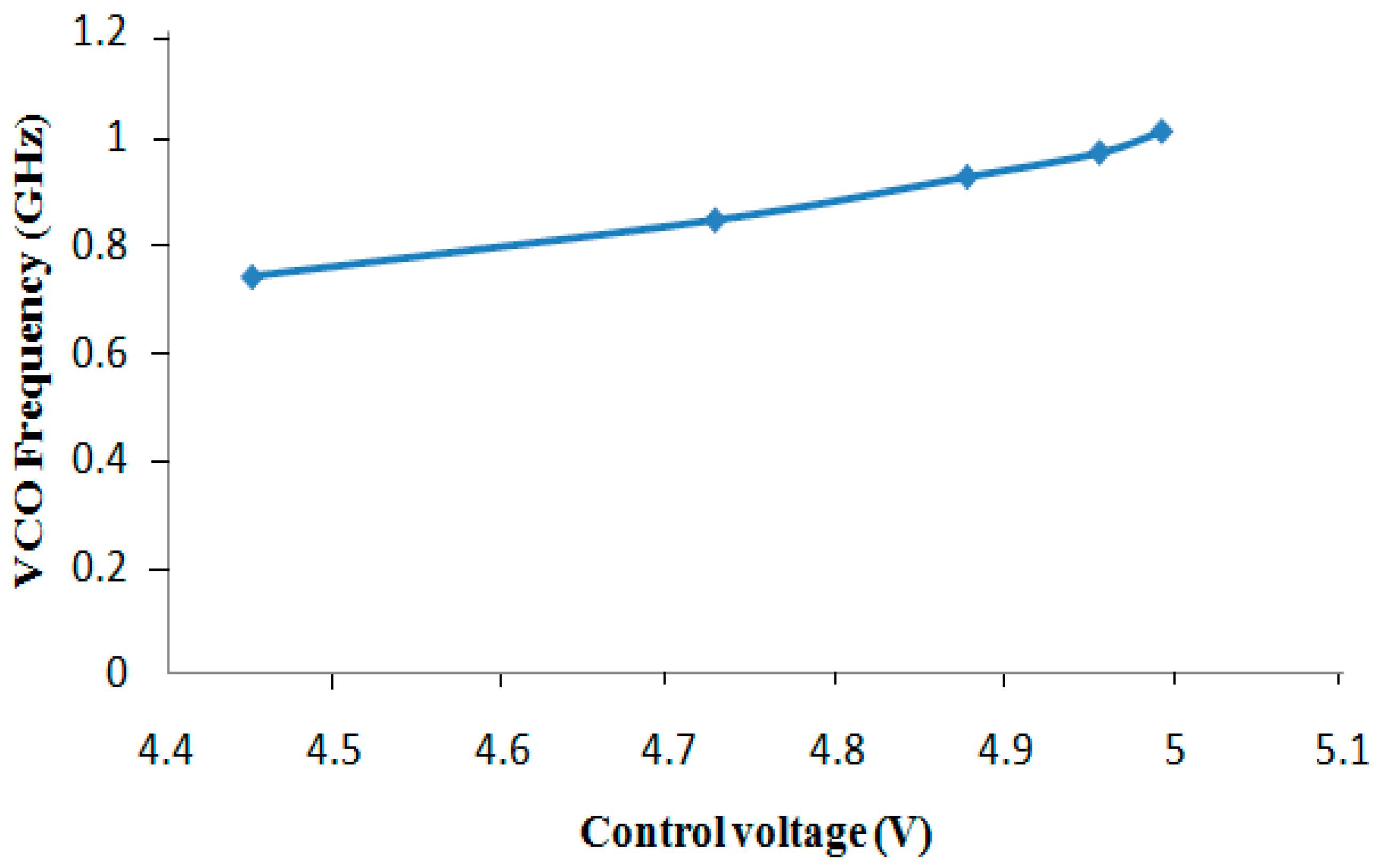
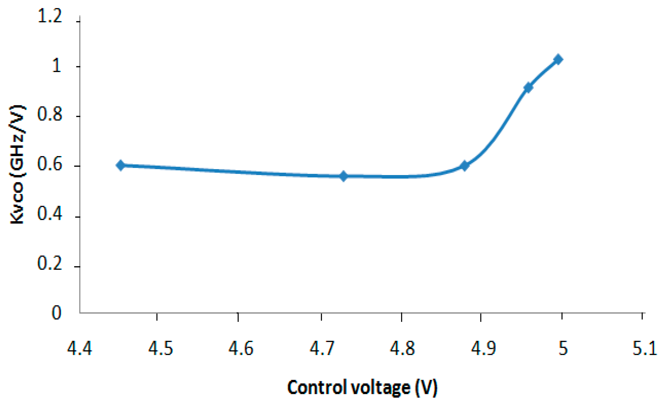
4. Results and Discussion
5. Conclusions
Author Contributions
Funding
Conflicts of Interest
References
- Boulghassoul, Y.; Massengill, L.W.; Sternberg, A.L.; Bhuva, B.L. Effects of technology scaling on the set sensitivity of RF CMOS voltage-controlled oscillators. IEEE Trans. Nucl. Sci. 2005, 52, 2246–2432. [Google Scholar] [CrossRef]
- Nicholas, H.T.; Samueli, H. A 150-MHz direct digital frequency synthesizer in 1.25-µm CMOS with-90-dBc spurious performance. IEEE J. Solid State Circuits 1991, 26, 1959–1969. [Google Scholar] [CrossRef]
- Loveless, T.D.; Massengill, L.W.; Bhuva, B.L.; Holman, W.T.; Witulsk, A.F.; Boulghassoul, Y. A hardened-by-design technique for RF digital phase-locked loop. IEEE Trans. Nucl. Sci. 2006, 52, 3432–3438. [Google Scholar] [CrossRef]
- Kyriakides, E.; Carrara, S.; De Micheli, G.; Georgiou, J. Low-cost, CMOS compatible, Ta2O5-based hemi-memristor for neuromorphic circuits. Electron. Lett. 2012, 48, 1451–1452. [Google Scholar] [CrossRef]
- Prodromakis, T.; Toumazou, C. A review on memristor devices and applications. In Proceedings of the 17th IEEE Internal Conference on Electronics, Circuits, and Systems (ICECS), Athens, Greece, 12–15 December 2010; pp. 400–408. [Google Scholar]
- Sahin, M.E.; Guler, H. The design of memristor based high pass filter circuit. In Proceedings of the IEEE International Conference in Electronics, Circuits and Systems, Batumi, Georgia, 5–8 December 2017; pp. 494–497. [Google Scholar]
- Chua, L.O. Memristor–the missing circuit element. IEEE Trans. Circuit Theory 1971, 18, 507–519. [Google Scholar] [CrossRef]
- Strukov, D.B.; Snider, G.S.; Steward, D.R.; Williams, R.S. The Missing Memristor Found. Nature 2008, 453, 80–83. [Google Scholar] [CrossRef] [PubMed]
- Zhu, G.; Singh, C. Improving students’ understanding research-based learning tools. Phys. Rev. Spec. Top. Phys. Educ. Res. 2012, 8, 1–8. [Google Scholar]
- Chua, L.O.; Kang, S.M. Memristive devices and systems. Proc. IEEE 1976, 64, 209–223. [Google Scholar] [CrossRef]
- Massmilliano, D.V.; Yurry, V.P.; Chua, L.O. Circuit Elements with Memory: Memristors, Memcapacitors, and Memductors. Proc. IEEE 2009, 97, 1–6. [Google Scholar]
- Barale, F. Frequency Dividers Design for Multi-GHz PLL Systems. Master’s Thesis, Georgia Institute of Technology, Atlanta, GA, USA, 2008. [Google Scholar]
- Razavi, B. Design of Analog CMOS Integrated Circuits; McGraw Hill: Boston, MA, USA, 2001. [Google Scholar]
- Razavi, B. Monolithic Phase-Locked Loops and Clock Recovery Circuits: Theory and Design; John Wiley & Sons Inc.: Hoboken, NJ, USA, 1996. [Google Scholar]
- Rajwardan, A. Design and Simulation of a Charge-Pump Phase-Locked Loop in 65 nm CMOS Technology. Master’s Thesis, University of Illinois, Urbana-Champaign, IL, USA, 2016. [Google Scholar]
- Gardner, F.M. Charge-pump phase-lock loops. IEEE Trans. Commun. 1980, 3, 1849–1858. [Google Scholar] [CrossRef]
- Johns, D.A.; Martin, K. Analog Integrated Circuit Design; John Wiley & Sons: New York, NY, USA, 1997. [Google Scholar]
- Sangho, S.; Kyungmin, K.; Sung-Mo, K.S. Memristor applications for programmable analog ICs. IEEE Trans. Nanotechnol. 2011, 10, 266–274. [Google Scholar] [CrossRef]
- Ascoli, A. Memristor-based filtering applications. In Proceedings of the 14th Latin American Test Workshop, Cordoba, Argentina, 3–5 April 2013; pp. 1–6. [Google Scholar]
- Zhang, B.; Allen, P.E.; Huard, J.M. A fast switching PLL frequency synthesizer with an on-chip passive discrete-time loop filter in 0.25-µm CMOS. IEEE J. Solid State Circuits 2003, 38, 855–865. [Google Scholar] [CrossRef]
- Wu, T.; Hanumolu, P.K.; Mayaram, K.; Moon, U. Method for a constant loop bandwidth in LC-VCO PLL frequency synthesizers. IEEE J. Solid State Circuits 2009, 44, 427–435. [Google Scholar] [CrossRef]
- Junsangsri, P.; Lombardi, F. Design of a hybrid memory cell using memristance and ambipolarity. IEEE Trans. Nanotechnol. 2013, 62, 1402–1411. [Google Scholar] [CrossRef]
- Djahanshahi, H.; Andre, C.; Salama, T. Differential CMOS circuits for 622–MHz/933–MHz Clock and Data Recovery Applications. IEEE J. Solid State Circuits 2000, 35, 847–855. [Google Scholar] [CrossRef]
- Ratan, R. Design of a Phase Locked Loop Based Clocking Circuit for High Speed Serial Link Applications. Master’s Thesis, University of Illinois, Champaign, IL, USA, 2014. [Google Scholar]
- Zhao, Y.-C.; Guo, Y.-C.; Tse, C.-K.; Feng, J.-C. Application of memristor-based controller for loop filter design in charge-pump phase-locked loop. Circuits Syst Signal Process. 2013, 32, 1013–1023. [Google Scholar] [CrossRef]
- Liu, Y. Phase Noise in CMOS Phase Locked Loop Circuits. Ph.D. Thesis, Louisiana State University, Baton Rouge, LA, USA, 2011. [Google Scholar]
- Minhad, K.N.; Kazemi, Z.; IbneReaz, M.B.; Jalil, J.; Kamal, N. Design of a current starved ring oscillator based VCO for phase- locked loop. Indones. J. Electr. Eng. 2014, 12, 1–3. [Google Scholar]
- Young, I.A.; Greason, J.K.; Wong, K.I. A PLL clock generator with 5 to 110 MHz of lock range for microprocessors. IEEE J. Solid State Circuits 1992, 27, 1599–1607. [Google Scholar] [CrossRef]
- Zhan, Y.; Kumar, S.V.; Sapatnekar, S.S. Thermally Aware Design. Found. Trends Electron. Des. Autom. 2007, 2, 255–370. [Google Scholar] [CrossRef]
- Pecht, M.; Lall, P.; Hakim, E.B. The influence of temperature on integrated circuit failure mechanisms. Qual. Reliab. Eng. Int. 1992, 8, 159–316. [Google Scholar] [CrossRef]
- Li, Y.; Wang, Z.; Midya, R.; Xia, Q.; Yang, J.J. Review of memristor devices in neuromorphic computing: Materials sciences and device challenges. J. Phys. D Appl. Phys. 2018, 51, 1–14. [Google Scholar] [CrossRef]


| Control Voltage (V) | VCO Frequency (GHz) |
|---|---|
| 4.450 | 0.741 |
| 4.726 | 0.846 |
| 4.876 | 0.926 |
| 4.955 | 0.971 |
| 4.992 | 1.010 |
| Control Voltage (V) | KVCO (GHz/V) |
|---|---|
| 4.450 | 0.594 |
| 4.726 | 0.550 |
| 4.876 | 0.592 |
| 4.955 | 0.908 |
| 4.992 | 1.022 |
© 2019 by the authors. Licensee MDPI, Basel, Switzerland. This article is an open access article distributed under the terms and conditions of the Creative Commons Attribution (CC BY) license (http://creativecommons.org/licenses/by/4.0/).
Share and Cite
Adesina, N.O.; Srivastava, A. Memristor-Based Loop Filter Design for Phase Locked Loop. J. Low Power Electron. Appl. 2019, 9, 24. https://doi.org/10.3390/jlpea9030024
Adesina NO, Srivastava A. Memristor-Based Loop Filter Design for Phase Locked Loop. Journal of Low Power Electronics and Applications. 2019; 9(3):24. https://doi.org/10.3390/jlpea9030024
Chicago/Turabian StyleAdesina, Naheem Olakunle, and Ashok Srivastava. 2019. "Memristor-Based Loop Filter Design for Phase Locked Loop" Journal of Low Power Electronics and Applications 9, no. 3: 24. https://doi.org/10.3390/jlpea9030024
APA StyleAdesina, N. O., & Srivastava, A. (2019). Memristor-Based Loop Filter Design for Phase Locked Loop. Journal of Low Power Electronics and Applications, 9(3), 24. https://doi.org/10.3390/jlpea9030024