Abstract
The continuous scaling needed for better performance and higher density has introduced some new challenges to the back end of line (BEOL) in terms of layout and design. Reductions in metal line width, spacing, and thickness require major changes in both process and design environments. Advanced deep-submicron layout design rules (DRs) should now consider many new proximity effects and reliability concerns due to high electrical fields and currents, planarization-related coverage effects, etc. It is, therefore, necessary to redefine many of the common DRs. For example, space rules now have a complex definition, including both line width and parallel length. In addition, new rules have been introduced to represent the challenges of reliability such as stress-induced voids, time-dependent dielectric breakdowns of intermetal dielectrics, dependency on misalignment, sensitivity to double patterning, etc. This review describes a set of copper (Cu) BEOL layout design rules, as used in technologies featuring lengths ranging from 0.15 μm to 20 nm. The verification of layout rules and sensitivity issues related to them are presented. Reliability-related aspects of some rules, like space, width, and via density, are also discussed with additional design-for-manufacturing layout recommendations.
1. Introduction
Device scaling, which has driven complementary metal-oxide-semiconductor (CMOS) technology for the last 45 years, increases not only transistor density, but also that of the metal interconnects at the back end of line (BEOL). Scaling in the BEOL means a reduction in the topological design rules (DRs) for metal line width and space, along with those for contact space (CS) and via width. In the vertical dimension, both metal height and via height are scaled down. This vertical and lateral scaling makes the manufacturing process more challenging.
In parallel with the geometric changes, new material requirements have been introduced. As copper (Cu) line width became smaller, line sheet resistance became higher. This required improvements in Cu metals, with the careful control of grain size, and the covering of Cu with a thin silicide layer [1]. One of the main concerns of BEOL performance was an increase in the resistance-capacitive (RC) delay of global wiring that was mostly dominated by the local (M1) and intermediate metal (MI) lines. For a reduction in parasitic capacitance, the dielectrics constants of both interlayer dielectrics (ILDs) and intermetal dielectrics (IMDs) were reduced with the scaling. However, integration and reliability challenges including thermally and mechanically induced cracking or adhesion loss, poor mechanical strength, moisture absorption, low electrical breakdown, and poor thermal conductivity limit a reduction in the dielectric constant [2,3]. A typical advanced BEOL (for example, 45 nm [4]) includes a first layer (M1), which is thin and has aggressive layout DRs in order to fit with the aggressive scaling of the front end of line (FEOL). Intermediate metal lines (MI, M2–M5) have similar or slightly increased thicknesses when compared with the M1 layer, and are mostly used for connections between various devices. Semi-global (M6–M7, 0.35–0.9 μm) and global (M8, 0.9–3.3 µm) lines are used for power buses, transmission lines, and inductors.
In order to achieve a tight pitch of M1 and semi-global lines with a high-density design, interconnects are used to connect high-density-logic transistors, standard cells, and other functional blocks in a system on chip (SoC). In general, application-specific integrated circuits (ASICs) and SoCs tend to use a combination of interconnect metals with a large number of MI lines (semi-global) for applications such as highly parallel graphics processing units (GPUs), field-programmable gate arrays (FPGAs), and multi-core smartphone processors (multiple central processing unit (CPU) and GPU cores). In contrast, devices for applications of radio frequency CMOS (RFCMOS), millimeter wave (mmWave), and WiFi use several layers of semi-global and global lines for inductors, transmission lines, and more. From a practical point of view, the set of rules relating to specific types of interconnect do not change based on their use in various applications. This is because many electronic design automation (EDA) tools such as design rule checks (DRCs), BEOL RC modeling, and even dummy fill insertions also need to be adjusted. Instead, the platform process design kit (PDK) includes a large set of metal combinations so that the designer may select one based on their integrated circuit (IC) needs. For example, WiFi ICs, designed using the 65 nm RFCMOS platform, will use a BEOL with eight metals overall, in which the M1 and M2 lines are local interconnects, the M3–M6 lines are semi-global metals, and the M7 and M8 lines are fat metals. The same 65 nm platform, used for general-purpose ICs, with six metals overall, includes the M1 line as a local interconnect, the M2–M5 lines as intermediates, and a global interconnect as the top metal. The total metal lengths and via counts (for example, for GPUs) continued increasing as technologies doubled their gate densities in each generation. Figure 1, based on data from [5], shows the relationship between metal wire length and the overall number of via increases, with respect to technology generations. At the point of the GK110 Tesla K20X GPU accelerator for high-performance computing (made by Nvidia), manufactured using 28 nm technology, there is a cumulative length of >20 km of minimum width interconnects, together with >10 B contacts, and >10 B vias. Naturally, these long metal lines (that increase by ×1.5–1.8 every generation), assuming that more than 50% have a neighboring metal line at the same level with minimum space in-between, introduce a major challenge for yield robustness. For this reason, several space rules have been set up for advanced technologies, as later shown. For vias, the increase in density (~×2 every generation), together with smaller via sizes, has introduced a demand for a new and larger set of via rules in order to check via density, metal-to-via space, and more.
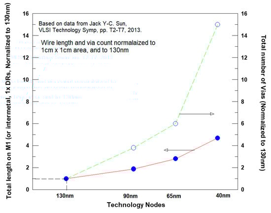
Figure 1.
Total metal lengths (for the first layer (M1) and ×1 metal design rules (DRs)) and via counts of graphics processing unit (GPU) devices, based on data from [5].
In addition, electrical parameters such as line resistance (nominal value and distribution) and reliability parameters such as maximum current density to eliminate electromigration (EM) are much more difficult to achieve. This results not only in requirements for better process integration and better materials, but also in more demand for layout design rules with supported EDA (Electronic Design Automation). Several books on the BEOL process and the related electrical and reliability aspects are available [1,6]; however, they do not fully cover the definition and setting of the layout design rules.
The aim of this paper was to systematically review some of the main BEOL DR, as used in the wafer foundry. For these rules, we reviewed the physical, electrical, and some reliability limitations that should be considered. While setting up the rule, emphasis was placed on some of the integration aspects related to the rule. This article is organized as follows: the methodology for setting layout rules is covered in Section 2 with several examples for metal space and via enclosure rules. Later, using this methodology, we provide examples and discuss various considerations for setting up contact rules in Section 3, followed by metal rules in Section 4 and via rules in Section 5. Reliability-related design rules such as metal width dependency on EM, via rules dependence on stress-induced voids and metal space rules that depend on time dependent dielectric breakdown, are discussed in Section 6. Design verification challenges and some aspects of BEOL next generation materials are covered in Section 7 and Section 8, respectively. A summary is presented in Section 9.
2. Methodology for BEOL Design Rule Setting
A comprehensive set of layout design rules should be defined by the wafer foundry for the use of the layout engineer, P-cell, and PDK Eng’s, as well as the designers that set up the place and route (P&R) design tools. The integrated platform set of rules should reflect the following considerations:
- (i)
- Technology process performance in terms of nominal process targets (like critical dimensions), as well as the accuracy requirement. Basically, the DR “limit” should reflect the “worst-case” process conditions. In practice, a large amount of process data should be collected and analyzed, including aspects of in–die wafer variation, die–to–die (D2D), wafer–to–wafer (W2W), and lot–to–lot (L2L) differences. In addition, to enhance manufacturing cycle-time, the production floor uses several process tools for each step. This is another important aspect that introduces variability.
- (ii)
- Sensitivity of the relevant electrical parameter to the process variation. For example, the dependence of the first metal “open” (un-connected M1 line) to M1 nominal width and variability. Some of the dependencies are very clear. However, some require integration of certain aspects of interaction between several layers. For example, the overall sensitivity of the via resistance depends not only on the via size (that is fixed in the design), but also on the enclosure of the metals below and above the via. A small via or insufficient metal enclosure below or above will result in higher via resistance. Therefore, in order to maintain stable via resistance, several rules should be defined.
- (iii)
- Sensitivity of the reliability parameter relevant to the process. For example, the effect of a very narrow M1 line on the maximum current allowed the elimination of working at the EM conditions.
- (iv)
- Scaling demands and manufacturing costs.
The DR development methodology should integrate the process data that comes from the manufacturing floor and the electrical and reliability data extracted from a dedicated set of development test chips labeled DRV (design–rule–verification) in this text. The DRV test chips consist of a set of similar structures with different dimensions for the relevant layout parameter to be tested. For example, the M1 space DRV (Figure 2) should include a set of inter-digitized combs with a similar M1 width at different spaces. Under-design rule spacing should also be included to check the process variability and the process window, and to provide information for the next generation technologies. Note, other factors should also be considered: the voltage applied for measuring the leakage, the parallel length along the lines, the layout pattern, and more. The experimental results of the local coverage and the contact or via slope angle are used to calculate the top and bottom critical dimensions. Other parameters such as the metal trench slope (see also Figure 16 later on), the layers overlay, etc., must also be considered. All these parameters are used for calculating “the worst conditions” under which the design rule should still be valid [7].
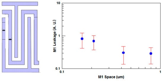
Figure 2.
Example for M1 space DRV (design rule– verification) rule setting: the comb structure (left) and the measured leakage under Vapp = 1.2 V (right). The overall parallel length was ~2 mm. For each space, data from ~160,000 sites were used.
Another example for DRV structure is shown in Figure 3. A dimensional sensitivity set was developed including 15 different layout parameters like via width and the side or the line-end enclosure of metal below or above the via and more. Careful analysis should be made in order to understand the proportional effect of each design rule on the overall via resistance. Such an analysis provides important process information, for example, the via/metal alignment limits, via width and metal width, and space min/max CDs. In some cases, a complete infrastructure that includes a complier is built in order to generate the DRV structures, as well as the related documents and the electrical testing scripts [8]. The methodology described above is slightly different from the one intended to link the physical design rule and the in-line metrology data for process control and monitoring [9]. The last one is based on the data extracted from PCM (Production–Control–Monitors) test chips that have a limited amount of devices, with min DRs (not using the set of layout rules). A combination of these data with physical parameters from in-line metrology is the basis for the analysis to find the physical-electrical correlations. Such information is very useful for process control, out-of-spec inspection, as well as the qualification of new processes.
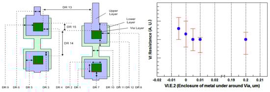
Figure 3.
Example for metal enclosure around via DRV test structure. (left) The 15 layout DRs to be considered. Adjustments were made to DR12 (right), the measured via resistance. Other parameters like metal side-enclosure, via width, metal width, and others were held constant (on min DR value).
3. Contact Related Rules
Contact plugs connect in between the first metal line (M1) and the silicon below; active area (AA) for oxide definition, (OD); as well as to the GC (gate control, poly). The connection should provide minimum resistance and excellent reliability performances in terms of current allowed passing through, with minimum area. In addition, the process must show high robustness and low cost manufacturing.
3.1. Contact Width and Space Rules
As MOSFETs are getting scaled, finer connections in between M1 to the diffusion (AA) and to the GC are needed. The contact-to-silicon (CS) is made through a thick dielectric layer (D1), having a Ti/TiN barrier metal around the W-plug. This fact introduces a process challenge of creating a very narrow contact hole with a high aspect ratio. For example, in 45 nm technology, D1 thickness was in the range of ~0.78 µm and consisted of a set of different layers such as SiO2 and Si3N4 (for the contact etch stop layer), USG (undoped silicon glass) as the main dielectric layer, and SiOC (as a dielectric etch stop layer). It had an aspect ratio of 0.78:0.06 (CS.W.1 in Table 1) that was >12. This is one of the main reasons that the contact width was given a singular value (a fixed width and length) in most of the design area.

Table 1.
Typical values for CS (contact-to-silicon) rules.
A scaling value of ~×0.75 in contact pitch was maintained for all copper technologies listed in Table 1. For contact space, where the contacts are arranged in an array, the minimum space should be set to slightly larger values (+10~15% over CS.S.1), in order to compensate for the local proximity and micro loading effects that take place during the exposure and etch steps, respectively. In order to have higher density, contacts that belong to the same net may use slightly lower space (CS.S.1) when compared to contacts at different net (CS.S.3).
The reduction in contact width introduced a challenge for contact resistance robustness: Figure 4 (left) shows the contact resistance as a function of the contact width. This data was extracted experimentally using similar structures that included different CS sizes. Naturally, larger contact yields lower resistance, which, in general for CS.W.1 ≥0.04 µm, is proportional to the increase in area. However, smaller contacts also showed significantly larger distribution. This fact became a challenge in advanced technologies, as seen in Figure 4 (right): a change of 6.5 nm (~15% from nominal CDs) yielded a change of +45%/−35% in contact resistance. In order to achieve the same magnitude of change in contact resistance for 130 nm~90 nm technology, the CDs should be reduced by half the size. In order to satisfy this aggressive demand, a superior process development consisting of state-of-the-art Ni(Pt)Si formation integrated with the contact process was needed to provide good yield of a 64 Mb SRAM array of a typical 28 nm qualification product [17]. The SRAM cell area was 0.127 µm2, with an average contact resistance of ~75 Ohm/contact, and upper and lower limits of 100 and 50 Ohm/contact, respectively.
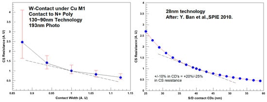
Figure 4.
Contact resistance as function of contact width (CS.W.1). Smaller value of contact increases contact resistance, as well as the contact resistance distribution. (left) Data of 130~90 nm technology and (right) data analysis of 28 nm technology based on [15].
3.2. Enclosure and Extension of Active and Poly around Contact
Contact landing on active must have enough AA enclosure all around (CS.E.1). A typical enclosure value is about 0.10~0.05 µm for 130~90 nm technologies, ~0.01 µm for 45 nm [14], and ~0.005 µm for 28 nm. This enclosure is needed to maximize the contact area landing on active to minimize the contact resistance. In advance technologies, the rounding of the AA edge should also be taken into consideration. To insure a full overlap, contact located at the AA corner may require a larger enclosure. Figure 5 shows this dependency: the electrical test structure consists of a long chain of AA/CS/M1-M1/CS/AA, similar in nature to the structure shown in Figure 3. The overall chain resistance was measured, and after reduction of the AA and metal resistance, it was divided by the number of contacts.
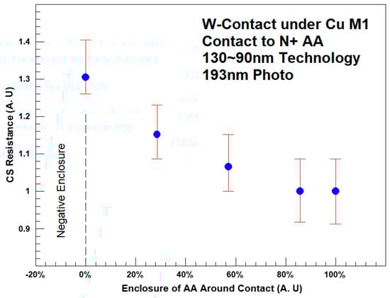
Figure 5.
Contact resistance as function of AA enclosure similar from three sides around the contact (CS.E.1).
The CS.E.1 value mostly depends on the CS–AA alignment that improves with technology generations. Due to the fact that the squared contact is a circle on silicon, in the case of no enclosure (CS touching AA edge) or even negative enclosure (some of the contact is outside the active), the contact resistance is still controllable. However, this situation may cause junction leakage: some of the damage introduced into the silicon during contact etch may accumulate at the AA/STI interface, and lead to leakage of the shallow junctions located below. In general, this mechanism is similar to the one that describes the effect of the damage, induced into the AA by spacer etch back, in case the poly (located over STI) is too close to the AA/STI interface [18]. This potential leakage is more severe for the case in which the CS is located near an AA corner that may also be rounded. This leads to a shorted effective enclosure. To solve this, in some cases, the single CS.E.1 rule is split into several rules considering the AA side enclosure, AA line-end enclosure, AA enclosure from opposite sides, neighboring to the AA internal (convex) corner, and more.
It was found experimentally that CS resistance landing on the N-type active area or N-type poly is dependent on the overlap of the M1/CS area as seen in Figure 6 [19]. An equation fitted to the experimental results provided the possibility of determining the resistance sensitivity (% change in R vs. % change in area) [18]:
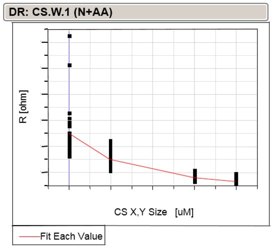
Figure 6.
Resistance of CS landing on N-type active area or poly as a function of the area.
The electrical structure consisted of a chain of M1/CS–CS/N-Type active area or poly. The slightly different coefficients between the two cases are related to the different barrier heights of the two systems.
Another layout rule for contact landing on the AA is the minimum distance to the butted diffusion edge, (CS.X.1/2). The terminology “butted diffusion” refers to the boundary were N+ S/D touches P+ S/D.
The nature of the contact formed depends on the doping level of the silicon under. For example, it is recommended for good analog Schottky diodes to place the contacts over lightly-doped silicon. This is because the tunneling of carriers through the junction (Schottky) barrier predominates on heavily-doped silicon, and the contact is ohmic. As a general ground rule for analog design, as many contacts as possible should be included in order to reduce parasitic resistance. Additionally, contacts should be placed using a “relax DR’s”, in order to eliminate any performance shifts due to leakages of stress (see for example, CS.D.1 and related stress effects, as covered below). For digital design, that high-density layout is needed, as in most cases all contact rules are set to the minimum and with a single contact. Double contact is included only for the case of no area penalty.
In cases of intermixing (i.e., overlap of the two highly concentration opposite type dopants), the native oxide grown on the top of the AA will be much thicker, and may not be removed during the standard pre-salicidation clean. As a result, poor salicidation will form, which results in a very high contact resistance for the case contact landing above. The same situation takes place for contact landing on the N+/P+ boundary over polysilicon. Figure 7 shows a poor salicidation over poly at the intermixing line, which yielded very high contact resistance. In some cases, the sizing of NSD (N+ S/D) and PD (P+ S/D) takes place to eliminate intermixing. To insure that the contact is landing only over salicide AA or salicide poly, dedicated layout rules (CS.N.1 for example: CS is NOT allowed to land on the salicide blocking layer) are set. This rule also checks the distance in-between the contact and the edge of the salicide blocking layer. As a ground rule, CS landing over the non-salicided area may have a ~×10 higher resistance vs. the same structure but salicided. In addition, maximum resistance (set by the 3σ distribution) is ~×6 higher than the typical resistance (~×2 at a similar but salicided structure).
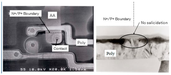
Figure 7.
An example for a failure due to high contact resistance related to contact located too close to N+/P+ boundary. (left) SEM top view; (right) TEM x-section, showing the poor salcidation formed over the poly due to relatively thick native oxide formed over the poly at the location of the N+/P+ boundary. This oxide blocked salicide formation.
The resistance of CS over N + AA is similar to CS over P + AA. For contacts landing on poly, the resistance is lower (~60%). Furthermore, for contacts landing on poly, there is a need to make sure that the poly encloses the contact from all sides (CS.E.2). Additionally, insufficient enclosure may yield degradation of the contact resistance. Contact-to-poly is allowed to land only over the poly that is outside the AA (poly–over–STI). This is due to the potential plasma damage that may degrade the thin dielectric gate below, causing degradation of the MOSFET or the MOSCAP performances. In addition, the contact-to-poly should be located more at the minimum distance to the STI/AA edge (CS.D.3). The aim of this rule is to ensure enough distance to the potential topography “step” of the poly at the AA/STI boundary.
3.3. Distance of S/D Contact to Related Gate (CS.D.1)
The design value of CS.D.1 at 130 nm~22 nm MOSFETs technologies is shown in Figure 8. Based on 0.13 µm as a reference, a factor of ×0.7 represented very well the scaling of this rule. On silicon, the CD uniformity of CS.D.1 is mostly dependent on the alignment of contact-to-gate and also on the values of the gate width and contact width. In addition, the real distance is also affected by the contact and poly shapes, contact CER (contact edge roughness), D1 thickness uniformity, and poly LER (line edge roughness), which all depend on the photo, etch, and CMP manufacturing steps. At technologies <45 nm, there is also a need to consider the mask distortion. For all technologies of high volume foundry production, the variation of site-to-site (S2S), wafer-to-wafer (W2W), and lot-to-lot (L2L) should be considered.
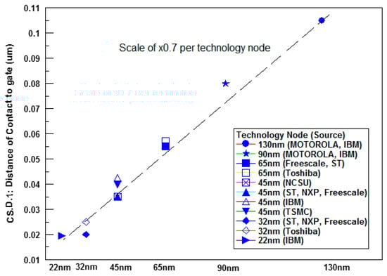
Figure 8.
Distance of contact gate (CS.D.1) for different MOSFETs technologies. Data were collected from [12,14,20,21,22,23,24,25,26].
The landing distance of S/D contacts and the related gate (CS.D.1) must be limited. Along the scaling, this rule received much attention as it has a direct and significant effect on the density, performance, and reliability of the MOSFET. Starting at 65 nm technology, the poly-to-contact parasitic capacitance had the largest contribution among all of the parasitic capacitance components [21]. In addition, any direct short or higher leakage between the gate and the S/D terminals resulted in significant degradation of the yield [27]. From a process point of view, the taper profile of the contact may have a marginal distance from the top of the gate. Therefore, good control of the dimensions and registration is a vital factor for both functional yield and SRAM leakages.
To effectively monitor the leakage current between the contact and gate electrodes, it was proposed to block the extension implant (during the mask generation by modifying the Boolean operation) at this monitor structure [27]. This eliminates any interference with the gate leakage through the extension doping inside the AA, as most of the voltage is supported by the depletion region under the spacer, even at low drain voltages.
Contact located too close to the poly gate may lead to higher contact resistance. This increase in resistance is due to the reduction of the area of contact landing on the salicided active, as part of the contact is located over the dielectric spacer and/or over the AA that is not covered with salicide. Figure 9, from 130~90 nm Cu technology, gives an example of the resistance dependence. The leakage value of the contact-to-gate (Figure 10) also depends on CS.D.1, the spacer width (~900 A in this case), and material, as well as on the contact shape: the leakage rises exponentially as the distance reduces. The voltage applied (3.7 V) developed a lateral electrical field inside the oxide/nitride hybrid spacer of <0.5 MV/cm.
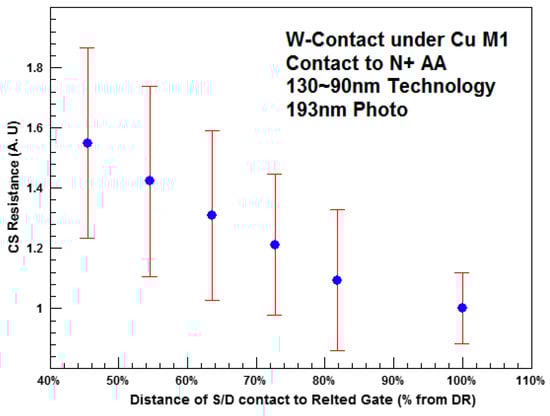
Figure 9.
CS resistance as function of CS.D.1; resistance increases as part of the contact landing over the spacer dielectric.
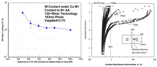
Figure 10.
(left) The dependence of contact-to-gate leakage on CS.D.1: shorter distance increases the leakage exponentially and (right) the contact resistance distribution for different values of CS.D.1 at the 65 nm platform [12]. The DR set to this technology was 0.05 um.
The reduction of CS.D.1 along the scaling introduced reliability concerns: dielectric breakdown along the time under Gate–S/D voltage drop at higher temperatures. A group from Renesas [28] investigated the voltage ramp dielectric breakdown (VRDB) and time-dependent dielectric breakdown (TDDB) for CS–Poly interlevel dielectric stack. The technology platform used was assumed to be 32 nm. Using constant voltage stress (CVS) tests, they monitored the leakage as a function of applied voltage and defined the lifetime when a sudden change (hard breakdown) was observed at Vapplied = Vbd. The results suggested that the conduction mechanism of CS-Poly was similar to that of Poole–Frenkel conduction. The median Vbd clearly exhibited area scaling, although the median electrical field to breakdown (Ebd, that is the slope of the line) was stable. The estimated etch bias determined by the x-intercept increased with the number of CS–Poly pairs. On the other hand, the estimated Ebd distribution did not show clear area scaling. Namely, the median Vbd area scaling should depend on the LOCAL deviation of the CS–Poly spacing. This is an important point, as the core design always uses the minimum CS.D.1 value, so the lifetime mostly represents the degradation dependence on the number of contacts and their size variability under Vapplied. The Ebd that represents the post-patterned breakdown field decreased with increasing temperature.
The overall effect of the location of the contacts related to the gate on the main MOSFET performances—drive current and leakage—was studied by [13,15,16,28,29] and found to mostly depend on three main parameters (Figure 11):
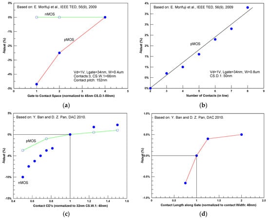
Figure 11.
The effect of contact landing on MOSFET performances: (a) the effect of distance of the contact-to-poly gate; (b) the effect of number of contacts, as adjusted by the contact pitch; (a,b) are for 45 nm technology, with dual cESL stressors and eSiGe for the pMOSFET. Analysis based on data from [13]; (c) The effect of contact area, as adjusted by contact CDs; (d) the effect of contact length (along the poly gate), with a fix contact area; (c,d) are for 32 nm technology. Analysis based on data from [16].
- (1)
- The distance of S/D contacts to related gate: the larger the distance of the contacts from the gate, the lower is the effective relaxation they induce into the stressed layer [30].In most cases, stress enhance techniques for the nMOSFET used a tensile stressed liner made of nitride that also used as the soft contact etch stop layer (cESL). For the pMOSFET, a compressive linear, together with embedded SiGe (eSiGe), was used (see for example [16,31]). Placing a contact over the S/D area means “punching” the stressed layer, which gives local relaxation to the stress. The closer the contact’sto the related gate (smaller CS.D.1), the higher the effect of the stress relaxation. Due to the fact that the mobility modulation was much higher on pMOSFET when compared to nMOSFET, the effect of pMOSFET was much higher.
- (2)
- Number and the overall area of contacts located between poly gates: a larger number of contacts results in more relaxation of the cESL stress. The contact shape (for the same area) also had an influence. In this case, the current variation of nMOSFET was due to CD variation (area variation), and was found to be more sensitive to that of pMOSFET because of the different resistance dependence [16]. The contact shape was also an important parameter; as the contact length along the gate line was larger (for the same contact area), the saturation current was increased. The main reason was that longer contacts (parallel to the gate) with the same contact area yielded less current crowding from the S/D electric field with similar stress relaxation of the liner [16].For many years, a common guideline for all the technologies recommended the insertion of “double contact” or “redundant contacts” or “as many contacts possible, w/o violating the layout DR’s”. However, for 65 nm technologies and below, which extensively use different types of stressors, such a guideline needs to be modified. New rules and guidelines that specifically define the number of S/D contacts as a function of the transistor width were listed and coded. This is most important for the S/D contact in PMOSFET core that included the eSiGe that does not have a perfect planarity. The P-cell used during design should specify the exact location (CS.D.1) and number of contacts with exact pitch. In addition, during the LPE (layout parameters extraction) step at the design flow, more layout information, including the exact S/D contacts location, was extracted.
- (3)
- Poly pitch: the larger the poly pitch, the higher the stress induced to the channel by the cESL layer until reaching saturation [28]. This stress was not uniform along the poly space and increased toward the center. For nMOSFET, the larger the Poly–Poly space, the higher the mobility enhancement until saturation was reached. However, the overall enhancement was limited to ~5% for 45 nm and <~2% for 20 nm [29]. For pMOSFET, a tight poly space also reduced the enhancement induced from the cESL. In addition, the smaller eSiGe volume also reduced the stress in the channel. The performance enhancement for pMOSFET was ~12% and 10% for 45 nm [13] and 20 nm [29], respectively.
At 65 nm technologies and below, restrictive design rules (RDR) are in use. The aim is to increase the ability to control the physical dimension of the pattern and to reduce variability (see for example [32]). Many times, this “conservative” approach has provided a first-time success rate. For the Poly layer, the introduction of dummy poly lines at a fixed width and pitch are mandatory. These dummy poly lines affect the stress induced into the channel.
RF performances of MOSFETs are also sensitive to the three parameters listed above [33]. For example, for 45 nm RFSOI technology with a CS.S.1 of 0.084 µm, an increase of CS.D.1 from 0.045 µm to 0.14 µm, together with a Poly space (GC.S.1) increase from 0.15 µm to 0.34 µm, improved the nMOSFET cut-off frequency from 280 GHz to 330 GHz. This improvement was due to the lower gate to source parasitic capacitance (Cgd) and higher effectiveness of the cESL liner. Additionally, tight CS.S.1 improved performance.
3.4. Non-Square Contacts
Long and narrow contacts showed improved performance of nLDMOSFETs at 0.13 µm technology over SOI, used for RF front-end module applications [34]. The “ribbon contacts” or “contact bars, CSBAR”, were used for Gate and Source terminals, and regular (square) contacts were used for the drain. fmax was improved from ~35 GHz to 80 GHz. CSBAR had a DR width (CSBAR.W.1) smaller than CS.W.1 (by ~×0.75) that ensured similar width on the silicon. Other layout rules for CSBAR were the minimum and maximum length (along the w of the MOSFET), space in between two CSBARs (similar to CS.S.1), and the distance between CSBAR to the regular contact. The layout rules for the enclosure of AA or Poly around CSBAR included relatively large values when compared with regular contacts. Other rules were dedicated to the space between CSBAR and regular contact.
Using long CSBAR also introduces process challenges: due to the relatively long contact “trench” inside the D1 layer, stress that develops during the following heat treatments can lead to abnormality in contact shape and become potentials for contact-to-contact shorts. The abnormal shape depends on the D1 material (doped vs. undoped) and the post contact etch thermal budget. The plastic deformation that takes place during the heat treatment depends on the layout: several CSBARs located close enough will have a regular shape, as the stress is balanced between them. In an array of CSBARs, the central CSBAR will have a regular shape when compared to the CSBARs at the edge of the array. From a DR’s point of view, a group of CSBARs with a fixed width and length required the addition of at least two dummy CSBARs from each side to eliminate the problem.
In advanced RFSOI technology, the performances have been hindered by high external resistance due to the lack of an effective doping technique to form low resistance extensions. The conventional ion implantation tended to amorphize the entire thin SOI layer. Raised source/drain was needed for FDSOI to reduce source/drain and contact resistance. After forming gate and thin spacers, an in situ doped epitaxy was performed to create raised source/drain (RSD) to reduce S/D resistance and contact resistance [35]. For this purpose, the rectangular contacts were drawn with dimensions of width = X and length = 2X (X2X), in which the length was along the transistor width, and contacts to Poly had a regular square shape of width = length = X (or slightly larger: X ~ 1.5X). Having two contact sizes manufactured by two consecutives process steps requires extremely high accuracy alignment between layers, which is mandatory for achieving a high density core. From the DR’s point of view, in order to achieve an accurate rectangular contact size, the space in between two X2X contacts needs to be relatively large (~2 times the size of the contact in the same direction). In addition, the minimum distance in-between the two contacts needs to be maintained. More discussion and examples for non-square contacts can be found in [36].
3.5. Optical Proximity Correction for Contacts
Optical proximity correction (OPC) is typically applied to compensate for various types of distortions. The simplest approach to manufacturing contact holes is to use a rule-based OPC (RBOPC). In the simple version, a bias was applied on each contact hole, depending on its length and width. Neighboring contact holes were considered by specifying a lower limit for the remaining space after biasing. From the DRs’ point of view, two or more space rules were implemented: for the case of neighboring contacts below a threshold limit and above. A simple threshold limit could be defined based on two conditions: N and Z, in which N is the number of nearby contacts that interact with the area defined by the contact under analysis (CUA) sized-up by Z. For example, at 28 nm, that CS.W.1/CS.S.1 = 0.04/0.07 µm [15,16], we can assume N ≥ 3, and Z ≈ 2 × CS.S.1 = 0.14 um. However, exact values for N and Z should be set experimentally, as they have a strong dependence on the process conditions that set up the optical range. Based on this example (Figure 12, left), the space in between the three vertical contacts can be CS.S.1, as N = 2. In this case, the third CS will get closer to CUA (Figure 12, right), N = 3, and all three contacts around the CUA need to have a larger space of CS.S.2 ≈ 1.5 × CS.S.1. This larger space in between contacts is also needed to implement the desired MBOPC corrections. Under this simple definition, any array of contacts with at least 3 × 3 contacts must use CS.S.2. Furthermore, a single or double row of contacts do not need CS.S.2.
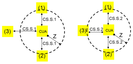
Figure 12.
Definition for CS.S.2. (left) As only CS #1 and CS #2 are inside the area defined by the contact under analysis (CUA) sized by Z/side, the contact space around CUA can be CS.S.1; (right) CS #3 is also inside, so all three contacts need to have a space of ≥CS.S.2.
The dependence on the neighboring contact is more complex. For technologies of 65 nm and below, in which the optical demands are more aggressive, the most common approach is to use off-axis illumination conditions (OAI) with attenuated phase-shift mask (att-PSM) and the insertion of sub-resolution assistant features (SRAF). However, using OAI can result in a “forbidden pitch”, a pitch that if used will yield a dramatic decrease of the depth of focus (DOF) with a narrow process window. Considering that the forbidden pitch range is usually semi-dense, assistant features cannot be applied for forbidden pitches under the optimized SRAF insertion rule due to limited space. If the SRAF must be applied for forbidden pitch ranges, the enhancement of the process window is limited, since the SRAF is not inserted at the most optimal location. Furthermore, this may introduce the risk of SRAF printing-out [37]. From the DRs’ point of view, additional rules of contact space should be implemented beyond the regular rule of minimum space (CS.S.1).
4. Metal Related Rules
Cu metal layers have been employed as the BEOL conductive layers since the 0.15 µm platform. Al was replaced given the lower sheet resistance and lower RC delay. This section discusses the different TDR related to metals. Examples for additional 45 nm rules can be found in [14].
4.1. Metal Width and Space Rules
The reduction in metal line width and space is an essential part of the scaling road-map. A scaling value (1/s) of ×0.75 between technologies was used (Table 2), in which s was the ideal scaling factor. Similar values were seen for the intermediate metal lines. Interconnecting lines, both local and global, were reduced by the same factor as the FEOL devices to reduce the gate delay by 1/s. In the quasi–ideal scaling of local interconnections, the horizontal dimensions are also scaled by 1/s to improve the overall power density and the packing density by a factor of s (≈1.4). In order to maintain a small RC value, the thickness was reduced by (1/), and thus the delay was decreased by (1/) [38]. Semi-global and global lines have similar thicknesses in technologies, and therefore they include similar line width and space DR requirements. Such a constant-dimension scaling of the global interconnections yields the rise of the propagation delay by sc2 where sc is the chip size scaling factor. For N10 (10 nm technology), N7 and N5, both M1.W.1 and Mx.W.1, were listed as 22 nm, 16 nm, and 12 nm, respectively [39]. The first Cu technologies did not use the “classical” ×0.7 Moore scaling factor in order to have a drawing dimension that was slightly larger in line or space. This was done to provide a process bias with the “design intended” dimensions on silicon. However, for advanced technologies, more critical constraints should be considered at the design stage or during mask date preparation. Designers and mask engineers must ensure that no errors due to snap–to–grid were made. For example, using the exact scaling of ×0.75 for the case of M1.W.1 = 0.09 µm at 65 nm will yield 0.0675 µm, which requires a grid resolution of 1/10,000. Working with such a fine grid results in a very large GDS file. For this reason, the typical scaling to 45 nm did not use the exact 65 nm values scaled by ×0.75.
Table 2.
Typical values for metal (all types) thickness, inter-metal dielectric (type, k) width, and space rules.
Metal Line Width: Based on classical resistivity size effect, the resistivity of polycrystalline metallic thin films increases when film dimensions (width and/or thickness) are of the order of the electron mean-free path due to surface, grain-boundary, interfaces, and defects scattering of electrons. The surface scattering contribution is the result of diffuse scattering of conduction electrons at the conductor’s exterior surfaces. The grain boundary scattering depends on the direction of the current flow related to the grain boundary, and this is the main driving force to carefully control the grain orientation during the process and working to have the largest grains possible (see for example, Chapter 9 at [6]). In addition, the process-related effects such as grain orientation, anisotropy, and line edge roughness also degrade the resistivity. Therefore, the reduction in width and thickness of the metal lines along the scaling path increased the sheet resistance. Example of the dependence of sheet resistance on line width can be seen in Figure 13. Kitada et al. [42] investigated grain size distribution dependence on the line width and height of 45 nm and 32 nm copper lines. They found that the grain size was proportional to the logarithm of the line width. Their results also showed that the grain size became smaller with decreased line thickness. Based on that, a thinner and narrower metal line results in a lower grain size and more grain boundaries that increase the Cu resistivity and resistivity variability due to larger boundary scattering. The mean free path of electrons in Cu is 36~40 nm at room temperature, explaining the rapid increase in resistivity at lines having width and/or thickness below this value. In addition, the calculations that used the first principles density functional theory (that is based on the electronic structure of Cu) found that even in the absence of scattering due to grain boundaries, edge roughness, or interfaces, quantum confinement was the root cause for the severe increase in the line resistance of Cu wires. More details can be found elsewhere [43].
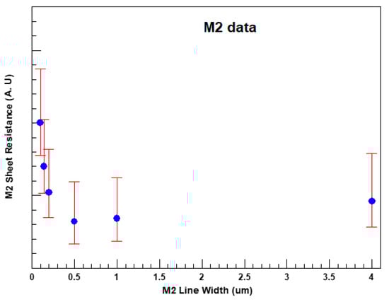
Figure 13.
Example of the change in sheet resistance as a function of the line width (data for 300 nm Cu thickness, 65 nm~32 nm technologies). The slight increase in Rs for lines wider than 1 µm is related to coverage effects and will be discussed later.
The solution for this line width effect can be found in several ways: first, by process improvement using a low resistance Cu alloy [5] or by using a CoWP cap layer or interface salicidation that were originally introduced for better EM performances [44,45]. More information on process solutions is given in Section 8 of this work. Second, by including this Rs(Width) dependency on the BEOL RC extraction tools for accurate modeling. From Figure 13, one can extract a simple layout guideline: for a critical signal line that requires a very stable resistance value, a line width >0.5 µm is recommended.
All Cu technologies (as well as the Al technology previously used) include layout rules for the maximum line width. In addition, lines with a width and length above a certain value, for example, W > 12 µm and L > 30 µm, required metal slits. The aim of the metal slits was to eliminate the possibility of delimitation (layer separation) between the Cu line and the oxide below or above, due to different thermal expansion coefficients between the different layers. For 65 nm technology, the line width was limited to ~10 µm, and in more advanced technologies, width limitation was reduced to ~4 µm. Due to this line width limitation, no metal slits were needed. The effect of line width on EM will be discussed later in more detail.
In case the metal lines do not match a 0/90 grid, they must be drawn on 45 deg. Other orientations are not allowed due to complications during the DRC, OPC, and mask fracturing. In addition, the 45 degree line segment needs to be longer than the minimum width (Mx.W.2 ≈ 4∙Mx.W.1). This is to eliminate cases of snap-to-grid during fracturing. Another reason for this limitation is the simplicity during OPC, which is mostly calibrated for 0/90 structures, and may require complicated corrections for 45 degree lines. Complementary rules for CS and vias located below and above the 45 degree metal lines are listed. For example, ensuring a larger metal enclosure.
Metal Line Space: The reduction in line spacing along the scaling path (Table 2) increased process complexity and the probability of metal shorts. In addition, the reliability tests for IMD–TDDB (time depended dielectric breakdown) depend very much on the metal spacing. We elaborate more on this reliability test in Section 6. In general, the probability (or the sensitivity) of failure due to metal shorts that result from a “killer defect” depends on three parameters: the metal spacing (S), the type and the defect density distribution of the killer defect, and the parallel length (L) between the two metal lines. Assuming the defect density distribution has a power of two dependency of the number of particles of a given size, we can define a “rule-of-thumb” for yield impact due to metal shorts:
in which K is a normalized parameter. Based on that, in order to reduce the critical area, it is highly recommended to have larger spacing for long parallel lines, as it reduces the sensitivity to metal shorts. This is done either by a hard layout rule in the design manual or by recommendations in the design for manufacturing manual. More detailed explanation on critical area calculation can be found, for example, in [46]. Several EDA tools for calculating the critical area and the predicted yield are used by the wafer foundries [47]. A very basic design guideline is to try to eliminate Vcc and Vss lines running in parallel; for a specific metal line, it is better to layout all of the Vcc lines one near the other and with relatively a large space-to-ground gap all the Vss lines together.
The use of parallel length as a second condition for some rules (see for example Mx.S.2, Mx.W.2) provides the flexibility to split the hard rule to several hard rules and increase the density.
Additional rules for metal spacing are set based on the line width (Mx.S.2, Figure 14): lines with large area (both width and parallel length) increase the probability of metal shorts due to the CMP (chemical–mechanical polishing) process sensitivity. Since Cu is softer than the oxide, it is polished more easily. When wide metal lines have only a small space of oxide between them, there may not be enough resistance to the polish, therefore yielding a faster removal rate than intended. Without enough space to provide strength to the configuration, the two metal lines may short. The foundry defines the minimum space based on the experimental results combined with CMP modeling. For coding simplicity, in many cases, the line width and the parallel length are set at the same value. Furthermore, for coding simplicity, the rule refers to the case when either side is wide, although the probability of shorts is doubled or even more in cases in which both sides are wide.
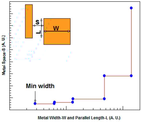
Figure 14.
Example of metal spacing rules that are set up based on line width and parallel length. Larger space is needed in case of wide metal and/or long parallel length in order to reduce the possibility of metal shorts due to the CMP effect.
Space to a line located at 45° (Mx.S.3) should use a much larger value when compared to the other rules (Mx.S.3 ≈ 3 × Mx.S.1). The main reasons are similar to Mx.W.2—a potential space reduction due to snap-to-grid and a challenging OPC.
One of the problems in applying this set of rules is presented in Figure 14. For example, if the line width is slightly below the value of the next “bin” space rule, the narrow space will be allowed even though it may increase the sensitivity to metal shorts.
Based on that, some EDA tools were developed, including the “equation–DRC” [48]. This provides the possibility of defining the space to be checked, based on the line width. The rules for minimum spacing between metals also depend on the “metal pattern” or “metal configuration”. Due to strong photo and etch proximity effects, enhanced line end shortening (LES) takes place for narrow lines [49]. LES is very problematic in cases in which contact (CS) or via are located at the line end as discussed later. In most cases, some of this shortening is eliminated using OPC (optical proximity correction) made by the wafer foundry during mask data preparation. However, in some cases, such a correction is limited. Figure 15 presents two typical cases: the left side shows two isolated lines at a minimum width. The tip-to-tip space can be set to the minimum, as the OPC correction is implemented on the tip sides. The structure on the right side is more challenged: due to the fact that the two middle lines are “dense” (having min space to the right and left lines), no OPC correction can be added on the tip sides. If OPC is implemented on the tip edge (in between tips), it may cause metal shorts. Based on this, new space rules should be set up specifying larger tip-to-tip space or larger space to the right and left. In fact, these additional space rules have been set for many more unique cases of line end close to the octagonal line in a “dense environment” that cannot allow an accurate OPC [50].
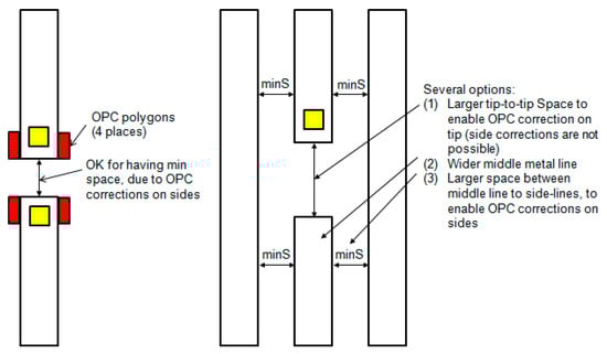
Figure 15.
Example of some metal patterns that have large sensitivity to shorts due to strong proximity effect and limited OPC. Such cases require dedicated space rules.
Additional metal space rules are related to the voltage difference between the two metal lines of two different nets (Mx.S.4). For larger voltage differences, a larger space is required. A higher voltage drop between the two lines increases both the electrical field and the probability for high metal-to-metal leakage, lowers IMD TDDB, and, in extreme cases, causes breakdown. As a ground rule, the space is set to eliminate electrical fields ≥1.5 MV/cm. Additionally, with this rule, the required space is also dependent on the parallel length in between the lines.
Some of the rules described above introduced a challenge for cell abutment during placement: cell-to-cell interaction caused lithographic hot-spots [51]. In theory, all possible cell-to-cell interactions should be characterized. However, advanced libraries include >1000 different cells, so analyzing all the overall placement combinations (at least 2 × 10002) is problematic. Instead, a pre-screening procedure followed by optimization based on a critical area analysis algorithm has been proposed. To test this method, a design that included 20,000 standard cells was used. Yield improvement of ~0.7% (beyond 98% before optimization) was shown [52].
As described above, new “sets” of space rules (described in Figure 14 and Figure 15) were originally made as “Yield Enhancement Rules” or “recommended” DfM (design for manufacturing) rules. However, as technology continued scaling, many of these rules were converted to hard rules in the design manual, and are not just recommended anymore. Thus, the overall number of rules has increased rapidly along the scaling path.
For FPGA (field programmable gate arrays), all routing consists of prefabricated metal wires together with programmable switches to connect the wires to each other and to the circuit element input and output pins. Many constraints based on the DR listed above are used during the routing. In addition, coupling (mutual) capacitance (Cm) in between two unrelated metal wires must be minimized in order to not degrade the circuit speed performances. This constraint becomes more dominant as metal space is reduced by a factor close to ×0.70 from generation to generation. Although the capacitances to the metal below (Cb) and above (Ct) the signal lines are both reduced along the scaling (mostly due to reduction in the minimum width), the level of interference between two neighboring interconnect lines is increased, which is usually referred to as cross-talk. It is very important for M1 to, have the finest space in which to achieve high transistor density in SoC (system on a chip). Due to the RC effects, the reduction of space can introduce cross-talk noise that is a result of too high total wire capacitance. In general, this occurs when one or more of the neighboring lines act upon a line and yield an unwanted voltage spike.
A simple modeling for cross-talk [53] refers to two wires (Ma, Mb) from the same metal level having a minimum-space in between. A signal swing (ΔVMa) on metal track Ma causes a noise pulse (ΔVMb) on floating metal track Mb, as defined by:
Cground is the capacitance of Mb to the metal below and consists of bottom capacitance and fringe. The amount that one signal propagates into the other one through cross-talk can be represented by ΔVMb/ΔVMa. Using capacitance estimations for 130 nm~22 nm technology nodes [53], a value of 70% was calculated for 130 nm. That is, 70% of the switching signal propagated into the floating neighbor’s line. For 65 nm and 22 nm, the value degraded to 84% and 90%, respectively. Due to the fact that timing and cross-talk are closely related, they need to be addressed concurrently with the place and route and dummy fill insertion tools. This can be done in several ways, like increasing the spacing for signal lines, using a shielding (with optimized space) in between the individual bus lines, eliminating having dummy metals near and below the signal lines, and more.
4.2. Metal Enclosed Rules
The enclosure rules of metal around CS located below M1 and around VI, and located below MI and above it, were set to ensure good electrical continuity and to minimize the via/metal related resistance. Some of the rules that related to metal enclosure around the holes (contact or Via) were already described during the discussion on metal spacing. That is, the enclosure is also dependent on the metal space around it that experiences heavy proximity effects. In this section, additional aspects will be listed.
In general, the enclosure rules are divided into two parts: the side-enclosure of the metal over the CS (M1.E.1) or via (MI.E.1), and the line-end extension of the metal over the CS (M1.E.2) or via (MI.E.2). Due to the LES effects [49], the line end rule is much larger in comparison to the side enclosure rule. Due to the proximity effects, especially the metal corner rounding, both enclosures are important to minimize the resistance. In fact, the M1 area overlap of the circle CS or via is the most important parameter. However, for simplicity in both layout and EDA coding, it is recommended to use a definition that is based on the enclosure size and not on the area. Examining the minimum enclosure of M1/CS used along the technology scaling shows that no real “scaling” is done, but a tighter process control is usually applied to satisfy the high-density needs.
The minimum enclosure values were set based on the fab performance considering three parameters: the CS or via width distribution, the CD dimensions of the metal above or below, and the most important parameter, the overlay performance. The last parameter is even more critical for advanced technologies using double patterning [54].
The overlap area of metal over CS or via depends on two parameters: the on-silicon CS or via hole diameter, and the metal shape below or above. However, the metal shapes, as listed before, depend very much on the configuration and the photo and etch proximity effects. An example is shown in Figure 16; M1 was not fully enclosed in the CS area. In Figure 16, the M1 was surrounded by other (unrelated) M1 lines, and because of that, the OPC for the M1 line end was limited. Due to strong M1 LES, the overlap was not sufficient, as seen at the SEM top-view that was taken after the M1 etch step and before the Cu fill. In addition, the M1 profile at the line end had smaller dimensions at the bottom when compared to the line top. The result was a higher CS resistance, which caused a failure of the related library cell. As a ground-rule, overlap of ≥60~70% of the hole area is enough for full functionality. In fact, a single rule of M1 over CS using the “% area” criteria can replace the two M1.E.1/2 rules. However, such a rule is not usually included in the wafer foundry as drawn DRC, only at the internal inspection after OPC operation.
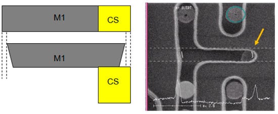
Figure 16.
An example for strong M1 LES causing an incomplete M1 enclosing of the CS. A cartoon top-view of the drawing data and the x-section showing the M1 bias (left). A SEM top-view (taken after M1 etch and before M1 Cu fill) shows that only ~50% of the CS area is covered by M1 (right).
Advanced BEOL copper technologies also use double patterning for metal formation [52,54]. Such a process scheme introduces additional variability of line-to-line and line-to-via that should be taken into consideration.
A systematic work to understand the dependence of CS resistance on M1 configuration and the related CS overlap was done by Shauly et al. [19]. A dedicated test chip that included about 650 different layout configurations at dimensions in one nanometer variation was used. The methodology flow involved a systematic edge contour extraction (ECE). Figure 17 shows an example of a structure with M1 enclosed CS below and unrelated M1 all around. In this example, the values of M1.E.1, M1.E.2, and the other layout parameters shown in the Figure 17 such as S1 and S2 = S3 were adjusted. The CS resistance was calculated on the basis of measurements of the M1 overlap area on the CS.
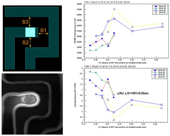
Figure 17.
An example for M1 configuration for testing the M1/CS layout rules [19]. The different dimensions used for analysis (left top), SEM top-view (taken after M1 etch and before Cu CMP) (left bottom), M1 overlap area (right top), and CS resistance (right bottom). Area and resistance are shown as a function of S1 and S2 = S3.
Larger S1 spacing increased the M1/CS overlap area and reduced the CS resistance. Enlargement of S1 by 0.02 µm reduced the contact resistance by ~30%, and the additional relaxation of S1 reduced the contact resistance even more. A significant resistance reduction was seen when S3 was increased (~24% for larger S3 by 0.05 µm). Based on such an analysis, and by using many other configurations, the wafer foundry set up the metal enclosure rules listed in the DR manual. A similar method was used in the development of the design for manufacturing (DFM) guidelines. These guidelines included rules for more relaxed dimensions that were recommended (but not mandatory). To reduce variability, some patterns were not recommended. In many cases, these recommendations were also coded. For example, the complex configuration shown in Figure 17 was recommended to have a slightly larger space for S1 and/or S2, S3. Sensitivity for other M1/CS configurations and some DFM examples were presented in [19].
The number of CS located under M1 affects the maximum current allowed to pass between the M1 and the active area. Kawasaki et al. [55] investigated the effect of additional contacts placed in line on the EM failure time of the M1 (Ti/TiN/Al-Cu/TiN stack). The normalized maximum current as a function of the number of contacts showed that two and three contacts increased the maximum current only by 35% and 69%, respectively. Based on that, a simple reliability rule was set so that the normalized maximum current allowed to be extracted from a line of n CS was only . It was also recommended to place the n contacts in parallel and not in line. A similar conclusion was also relevant for the via placement.
5. Via Rules
Via plugs connect between the metal line to the metal below. The connection should provide minimum resistance, excellent reliability performances in terms of current allowed to pass through, and minimum area. In addition, minimum manufacturing cost and high robustness should be assured. In Cu technologies, the via is made of Cu as part of the single or double damascene process integration.
5.1. Via Width and Space Rules
Reduction in via width and space is also a mandatory part of the scaling roadmap (Table 3). A scaling value of ×0.73 (×0.68~0.77) is used between technologies. For N10 (10 nm technology), N7, and N5, VI.W.1 was listed as 22 nm, 16 nm, and 12 nm, respectively [39]. With the reduction of the structural spaces in 45 nm technology node and beyond, topological effects in metal structures have become significant concerns for dielectric reliability. The impact of in-line overlay misalignment on the dielectric leakage and breakdown in some via related structures was studied by Liu et al. [56]. The experiment was done using a 45 nm platform with carbon-doped oxide (SiCOH) as the low-k dielectric material (k = 2.7), and using two types of via chains test structures: intertwined and face-to-face structures with pitches of 140 nm and 200 nm (Figure 18). The structures included M1, M2, and the via in between layers. TDDB measurements were performed using a stress of 4~6 MV/cm and temperature of 125 °C. The failure criteria was defined as a sudden increase by more than 2 order of magnitude in leakage current during stress. The modeling of failure distribution was done based on Weibull statistics that were expressed as
in which CDF is the cumulative distribution function, τ63 is time to 63.2% failure, and β is the shape factor. The model for low-k dielectric breakdown was used for failure time:
Table 3.
Typical values for vias (all types) width and space rules.
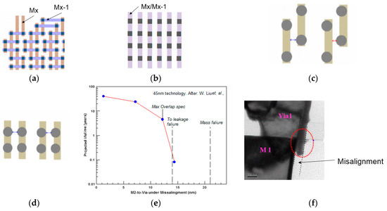
Figure 18.
(a) Intertwined via chain; (b) face–to–face via chain; (c) intertwined via chain: top-spacing is deteriorated directly by misalignment; (d) face–to–face chain: top spacing can tolerate misalignment partially due to via protrusions in both nets; (e) The TDDB life time dependence on M2 over via misalignment for the intertwined chain, based on data from [56]; (f) TEM showing one of the failure mechanisms related to the misalignment of via to metal under: the interface discontinuity and Cu out-diffusion yield short.
A is a fitting coefficient, is the model field acceleration factor, Vstr is the stress voltage, and s is the dielectric spacing.
There are four major process variables that impact the physical spacing of via chain structures. They are trench and via critical dimensions (CDs) variations, lithography trench–via overlay misalignment (MA), CMP non-uniformity-caused top spacing variation, and line edge roughness. Among them, overlay misalignment often plays a more important role: the variation of misalignment is larger by ~×2 than that of the trench or via CDs and directly reduces the dielectric spacing with via protrusion. For 45 nm, the edges of the misalignment distribution can reach ±0.2, represent 1~99% range of the distribution, and, for advanced technologies, this becomes a real challenge, since the absolute misalignment value is difficult to reduce due to tool capability limitations, wafer warpage, and more.
Analysis of the breakdown voltage results of the two chain structures is shown in Figure 18. The intertwined structure had a median of 28.5 V (vs. 33 V of the face–to–face chain) and larger distribution. The lower breakdown voltage can be explained by the smaller physical top spacing mean (50.2 vs. 53.8 nm) for the intertwined via chain due to smaller design space. On the other hand, the larger top-spacing standard deviation of the intertwined via chain indicates a significantly wider variation range, which accounts for the poor shape factor in the Vramp test results. This can be explained by the layout difference (Figure 18c,d). Unlike the intertwined via chain, the minimum top spacing of the face-to-face via chain was mainly determined by the protrusion profiles of two adjacent vias, and hence was less affected by the in-line trench-to-via misalignment. The TDDB life time dependence on M2 over via misalignment for the intertwined chain is also shown in Figure 18e: to avoid reliability concern, a reasonable lithography overlap spec should be set for misalignment around 12.2 nm and also consider the 3σ value of ~6.9 nm.
Naturally, if the misalignment is too large, early breakdown at low voltage takes place, especially in the face-to-face chain with larger via density. Two failure mechanisms have been found for such a case [56]: The first mechanism is related to the via to bottom layer (via to metal under) misalignment, which caused the via bottom discontinuous and hollow area, due to one side via etch through into the bottom dielectric (Figure 18f). Hence, Cu diffusion or moisture could cause a leakage path in the weak cap-layer/low-k/Cu interface. The second mechanism is related to the via to upper layer misalignment (metal to via under), which caused some planarization filling material to remain on one sidewall post trench etch process. Hence, the subsequent ashing process would generate excess polymer residues near the sidewall. If the wet clean process is not sufficient, some remaining minor residues would exist on the sidewall or drift to the wafer surface and cause the leakage path formation. This mechanism was also proven by the elimination of the early leakage population using improved wet clean process, as elaborated in [56]. For this reason, some dedicated DR (Vx.D.1) were set to ensure space between the via and another unrelated metal layer of another net: Vx.D.1 > (Via.E.1 + Mx.S.1) is large enough.
5.2. Double Via and VIABAR Rules
A very “popular” layout guideline is to have “via redundancy”. That is, two vias are included at locations that ensure that if a single via is in use, the design passes the DRC successfully. The driving force for using this guideline is to reduce the risk of disconnection due to via failure (via open). However, in advance technologies, using such a guideline is a challenge, as the DRs are very complex and the layout area is very limited.
With advanced technologies, in addition to the square via (of W × W), a rectangular via (or viabar) of fixed dimensions of 2~3 W × W is in use. This viabar has a smaller area when compared to two vias, and has the potential to give robust results in reliability testing when compared with a single via design. Semi-global and global vias have almost similar ILD thicknesses among the technologies, and because of that, they also have similar via width and space. In many cases, the VIABAR is inserted, during routing, or later on, by a dedicated insertion utility [61]. An example is shown in Figure 19. It includes four connections: M3-M2, M2-M1, M1-M2, and M2-M3. In this example, the terminology used was the one chosen by many fabs: Vxy, in which x and y represent the metal number below and above, respectively. Among the four connections, three were replaced by VIABAR. The utility also expends the metal below or above, to ensure the full enclosure of the metals around the VIABAR. In general, the VIABAR insertion utility algorithm has the following steps:
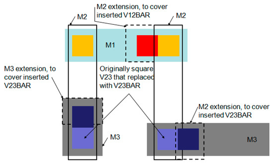
Figure 19.
An example for design after applying the VIABAR utility. Three out of the four via connections were replaced by VIABAR. The related metal below and above was extended to ensure the full enclosure of the metal around the VIABAR.
- Step-1:
- Mapping of the different nets, and finding out all square single vias (“lonely via”),
- Step-2:
- Replacing the square via with VIABAR,
- Step-3:
- Checking for structure validity. For example, that the VIABAR is not too close to another via. In case of a violation, go back one step, and change via placing,
- Step-4:
- Ensuring coverage of the metal below/above over the VIABAR. This step is done, by stretching some of the metal (Figure 19),
- Step-5:
- Checking for structure validity. For example, the stretched metal may cause Mx.S.1 violation. In case of a violation, do not stretch the metal and go back to Step 1.
The utility success criterion is the VIABAR yield—the percentage of square and VAIBAR in the design out of all vias. For example, in the ST 28 nm process, 15% of V12 were replaced to VIA12BAR, 12% for V23BAR, and 2% for VIA34BAR [61].
6. BEOL Reliability Related Design Rules
Naturally, many of the rules listed above such as metal-to-metal space are also related to the reliability; a larger space reduces the probability of failure due to metal-to-metal shorts when the device is used. However, a direct test of the time-to-failure as a function of the applied voltage and temperature should be done including statistical considerations. In general, three main reliability tests are done for BEOL qualification and characterization, in which the data is analyzed and set as “Reliability Guidelines” in the design rule manual:
- (1)
- EM tests check the maximum current allowed to pass through a metal line or metal interface (CS/M1 for example). The lifetime (LT) or mean time to failure (MTF) is a function of width, temperature, and the current applied [62]. After analysis, this value was set as the design guideline and included in the design manual.
- (2)
- Stress migration (SM) tests check for any abnormal shift in metal line resistance due to stress generated from the IMD around. These results are used to set up rules related to the number of vias needed to connect two metal lines based on stress induced voids (SIV [63]), failure that is discussed in detail later.
- (3)
- Time-dependent dielectric breakdown (TDDB) tests for the IMD check for any abnormal leakage between two metal lines as a function of temperature and electrical stress [64,65].
- (4)
- After qualification, the data for SM and IMD-TDDB are no longer needed as design guidelines or “rules”, unless the application requires overdrive conditions such as higher maximum temperature or maximum voltage applied.
6.1. Maximum Current Density in Metal Wires and Holes under DC Conditions
EM is a Cu atomic flux generated by extensive electron scatter (electron wind). The electric field applied across an interconnection during operation affects the net motion of metallic ions in the direction of the electron flow (i.e., from the cathode to the anode). This net flux of atoms is caused by EM, and can be described as the self-diffusion of metallic ions in response to an electric field [66].
The atomic flux is mainly the result of two opposing driving forces: the electron wind force that moves the ions in the direction of the electron flow, and a back stress that pushes the ions in the opposite direction [1,67]. From a design point of view, information on the metal width needed for the related current level, current mode (DC or AC) to be applied, and the application temperatures are needed. For DC conditions, the wafer foundry provides the max current density (Jmax_DC, mA/um) needed to achieve a lifetime (LT) of 100,000 h for a 0.1% failure rate at the maximum operation temperature [68]. For automotive applications, this criterion is changed depending on the automotive grade in use [69]. As a common practice for automotive applications, the criterion is set at a longer LT (15~20 years, for example), but with a duty cycle of 5~15% (depending on the mission profile) and with a similar or more aggressive failure rate at 125 °C depending on the grade. Rules at other temperatures are given for different mission profiles [70].
In order to extract theses values, a set of tests were done under extreme conditions (high temperature and high current density). In these tests, the wire resistance was monitored. The test structure consisted of a long metal wire (>250 µm, reasons explained below). The failure criteria were defined by the percent of resistance change. The appropriate failure limits, e.g., 2%, 5%, or 20% resistance change, were set according to the functionality specification for the technology [68]. These results were scaled back to common operational conditions (125 °C, for example) and listed in the platform design rule manual.
LT and Jmax_DC modeling are commonly done at the wafer foundry based on Black’s Law [66] with the relevant adjustment to the following specified failure rate:
in which A is an empirically-determined constant and MTFtest is the LT achieved in the test temperature (Ttest) and current density (Jtest). Tuse is the temperature in common use (125 °C, according to the design rule manual), kB is the Boltzmann coefficient, σ is the deviation in time–to–failure, and N is a constant that relates MTFtest to the desired failure rate (N = 3.09 for 0.1% failure rate, for example). Ea is the activation energy to EM failure, and n is the current density exponent. Typical Ea values for Cu technology are ~0.8 eV (0.7~1.0 eV). This range of Ea corresponds to failure due to atomic diffusion along grain boundaries (0.88~0.95 eV) and/or by surface diffusion along the interface Cu/Ta barrier metal [44]. Slight changes in Ea are related to line thickness and width, both of which affect the Cu grain size and grain boundary density. For example, we experimentally found that a value of Ea = 0.81 eV for a Cu thickness of 0.45~1.0 µm, and 0.76 eV for a thickness of 3.3 µm in the Cu layer. This value is supported by data shown in [44]. However, for simplicity, in many cases, a single Ea value is used for all Cu thicknesses and technologies. Typical values for n are between 1 and 2.
In many cases, the JDC__max values set in the design manual (Table 4) are lower compared to the values found experimentally. This is because of conservative considerations regarding statistical variation that may not have been approximated correctly in qualification tests, but is significant during mass production. Adjustments of JDC_max to higher temperatures were done using Ea and n, experimentally extracted in the foundry and provided in the manual. The rate (or slope) of JDC_max change vs. temperature was calculated using Ea/n/kB.
Table 4.
Typical EM JDC_max for different Cu technologies, and different thicknesses.
6.2. Setting-Up Design Guidelines for Metal Width on the Basis of EM Failures
Change in the width of the Cu interconnection while maintaining the current density and temperature does not significantly alter the resulting lifetime, especially in the case in which EM is mostly dominated by the diffusion path through the top surface [1]. This is in contrast to Al-technology, in which the microstructure plays a dominant role in the EM. It is commonly assumed that the activation energy for grain boundary diffusion is 0.88~0.95 eV, while for the dielectric/Cu interface (SiC/Cu interface, for example) it is only 0.80~0.90 eV. Grain boundaries that provide diffusion pathways are likely to play a negligible role because of the bamboo-like microstructure in the damascene trenches. Vairagar et al. [71] compared the MTF of M1 and M2 using test structures with line widths of 0.28 µm and 0.70 µm and a single via diameter of 0.26 µm under the same current density and temperature conditions. A reduction of approximately 25% in MTF was observed for M1, while for M2, a similar width effect did not exist. Both widths of M2 showed a similar current density exponent (1.2). They [71] correlated the results of M1 and M2 to the test structure configuration. In the M2 (upstream) test structure, current crowding caused a flux of vacancies from the high current density region to the low current density region located above the via. These voids seem to nucleate at the dielectric/Cu interface above the via and then grow along the dielectric-cap/Cu interface of the M2 trench. However, for the M1 (downstream) test structure, the peak current density was closer to the weak dielectric/Cu interface. Wider M1 has (or is expected to have) larger peak current densities at enhanced nucleation of voids under the via and a reduction in MTF. This sensitivity of the weak interface explained the Ea that was found for M1; 0.49 eV and 0.60 eV for a width of 0.28 µm and 0.60 eV, respectively. For M2, both widths yielded similar Ea values of 0.85~0.88 eV.
Lin et al. [72] also checked the effect of the line width on the EM performance using a structure connected with a single via. Careful analysis showed that for both M1 and M2, a wider line reduced MTF. They explained these results by the fact that Cu surface diffusion factor was more significant in the induction of the Cu migration in (or near, adjacent to) wide lines when compared to lines of minimal width. They concluded that Cu microstructure size was a second order effect.
Aubel [73] focused on the grain size effect on MTF, and showed an opposite dependence on line width: larger trench width increased MTF. Oates and Lin [74] showed that larger trench width reduced Jc (the critical length). That is, the relationships were complex: for short length, there was no significant dependence on width. However, as metal length increased, larger width improved MTF. Cheng et al. [75] also checked the dependence of MTF on line width (0.1 µm and up to 5 µm). They found for multiple via structures and narrow line widths, for example, a bamboo-like grain line; the contribution of the grain boundary diffusion was negligible because of the absence of a continuous grain boundary path. Therefore, the drift velocity of Cu line was a function of the metal line thickness and width, in cases in which the surface diffusion was dominant. So, the EM performance improved if the metal width or thickness increased. This is the reason why the EM resistance increased in the 0.1 µm~0.5 µm metal width range. Moreover, as the line width increased beyond the grain size, the impact of grain boundary diffusion must be considered. This resulted in an increase of MTF for designs that included metal widths larger than 0.8 µm. For structures using a single via, the line width dependence was very weak with relatively large distribution and with a strong dependence on via size: larger via size reduced MTF. Ko et al. [76] also found a MTF improvement of ×3.35, while metal width increased from 0.14 µm to 3 µm. This complex model is explained later after the discussion of the EM dependence on metal length. It is worth mentioning here that many foundries include a layout rule that limits the maximum width of the metal wire to a value of 10~20 µm. The reason for such a rule is not related to EM. The motivation is that in a wide line with a length of a few microns, the stress due to different thermal expansion coefficients at the oxide/metal interface is very high. In the past, complementary rules for slits insertion were provided. However, such slits increased the wire sheet resistance, and are suspected to have caused some difficulties in RC modeling, and may initiate cracks at the IMD. Therefore, they are not in use in advanced technologies.
The failure sensitivity under EM conditions does not depend only on Jmax or metal width. It also depends on the wire line length (L). As material diffuses towards the end of the line, it creates back stress, which reduces the driving force for EM. In other words, the electrical driving force is balanced by the compressive stress gradient, which causes an equal but opposite driving force [64,66]. The constant (jL)c was temperature-dependent, and its value increased with a decrease in temperature [77]. In other words, for short interconnects (L < Lc), the back stress is higher and the tendency to EM is reduced, ensuring longer LT. Experimental research indicates a rather wide range in the value of these criteria, with JDC_max. Lc ranging from 1500 to 5000 A/cm [78].
Overall analysis of width and length effects, using the data from [73,74,75,76], provides the complex dependence for EM MTF (Figure 20): short L resulted in long MTF, irrespective of width. Longer L had shorter MTF due to stronger EM conditions, and a stronger dependence on width. Larger width meant larger grain size and longer MTF. However, width that was much larger than the average grain size may reduce MTF due to large surface only. The characteristics shown in Figure 20 can also be used to define some reliability guidelines for JDC_max, assuming the reliability tests are done using a test structure that consists of a long line 250~1000 µm with minimal width. The JDC_max extracted can be larger by 1.5~2 when compared with shorter lines (<10 µm) at the minimum width. For larger width and shorter length, JDC_max can be enhanced by an increase of widths up to 3 [74].
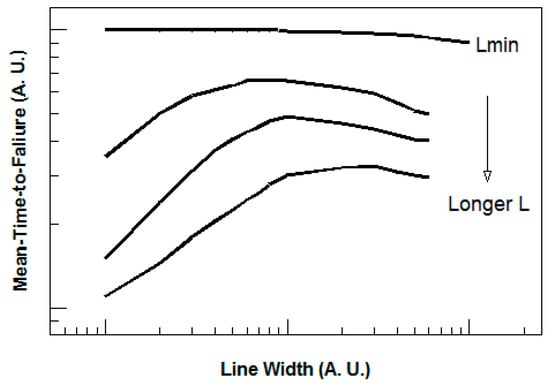
Figure 20.
A schematic description of the overall dependence of EM MTF on width and length.
7. Design Verification
The different types of DRs, some of them described in this paper, are made to eliminate any physical sensitivity to failure like metal line “open” or short, as well as to eliminate any reliability failure due to, for example, electromigration. As the lines and the holes become more sensitive to manufacturing variations, additional rules must be evaluated in combination to predict manufacturability, as the effects are multi-dimensional. Some of these checks are extremely difficult to code into the DRC (design rule checking) due to many different boundary conditions (for example, metal-to-metal space, as described in Figure 15—whether several different rules should be checked depend on the line end, line width, and the overall pattern). In addition, design rule count and complexity increase along the scaling path: for the 32 nm and the 22 nm technologies, more than 7000 and about 9000 rules are in use, respectively [48]. In parallel to the checking, a successful implementation of these rules into the platform P-cell library and into the P&R (place and route) is mandatory. Implementation of the relevant rules into the P-cell is followed by general DRC checking, OPC verification [50], and abutment testing [51] to “qualify” the cell as “DRC clean”. Finally, after placement, a full chip DRC is needed.
8. BEOL: Next Generation for Materials, Processes, and Related DRs
This reduction of contact width along the scaling (as described in Table 1) increased the contact resistance, yielding circuit performance limitation. From a process point of view, tungsten contact faces major scaling issues due to poor gap fill. As a replacement, copper contact metallization was investigated using CVD (chemical vapor deposition) Ru liner (or metal barrier, MB) for the 20 nm technology node [79]. No reliability issues were seen. The contact width (CS.W.1) was 35 nm [80]. The resistance of Cu vias increased rapidly toward the 7 nm and 5 nm logic technology nodes [39]. The main reason is that the MB scaling does not follow the overall via size reduction trend. Therefore, the tendency is to move to CVD Co. and Ru liners, which combine good step coverage with the added value that they enable Cu reflow methodologies to achieve the void free fills [81]. From a resistance point of view, the results are relevant for the 7 nm and beyond logic nodes. No drift of Co. ions into the dielectric was observed. This new contact and via prefill metallization strategy combined with alternative metals like Co. has become one of the most promising innovations for interconnects in future logic and DRAM technologies. Co-based contacts were successfully demonstrated for Intel 10 nm and Globalfoundries 7 nm platforms [82].
As explained in detail above, the dimensions scaling of the Cu-based process has degraded electromigration. As a replacement, three main alternatives can now be considered: Co and Ru, as well as Cu with Co cap showed highly reliable electromigration, with activation energies of 2.4~3.1 eV, 1.9 eV, and 1.5~1.7 eV, respectively [83]. These data provide a very promising solution for the BEOL of 10 nm and below platforms.
9. Summary
This paper systematically discussed different BEOL layout design rules. It covered different aspects of rule definition such as process, scaling, electrical performances, and reliability. For the main layout rules of line width and space, metal enclosure and via rules, it showed the relationships among the important parameters together with layout guidelines and examples. The analysis was conducted from the wafer foundry point of view, emphasizing the minimum design area and targeting the best performances.
Funding
This research received no external funding.
Acknowledgments
The author wishes to thank Eng. Israel Rotstein for endless fruitful stimulating discussions, Uri Krispil (Mentor Graphic Application Mgr, Israel) for great information and support for EDA utilities, and Amram Eshel for the linguistic review of this paper.
Conflicts of Interest
The authors declare no conflict of interest.
References
- Baklanov, R.M.; Ho, P.S.; Zschech, E. (Eds.) Advanced Interconnects for ULSI Technology; Wiley and Sons Publication; John Wiley & Sons, Ltd.: Hoboken, NJ, USA, 2012. [Google Scholar]
- Hau-Riele, C.S. An introduction to Cu electromigration. Microelectron. Reliab. 2004, 44, 195–205. [Google Scholar] [CrossRef]
- Havemann, R.H.; Hutchby, J.A. High-Performance Interconnects: An Integration Overview. Proc. IEEE 2001, 89, 586–601. [Google Scholar] [CrossRef]
- Ishmaru, K. 45 nm/32 nm CMOS—Challanges and perspective. In Proceedings of the 33rd European Solid State Circuits Conference, Munich, Germany, 11–13 September 2007; pp. 1266–1273. [Google Scholar]
- Sun, J.Y.-C. System scaling and collaborative open innovation. In Proceedings of the 2013 Symposium on VLSI Technology, Kyoto, Japan, 11–13 June 2013; pp. T2–T7. [Google Scholar]
- Yoda, T.; Miyajima, H. Advanced BEOL technology overview. In Advanced Nanoscale ULSI Interconnects: Fundamental and Applications; Shacham-Diamand, Y., Osaka, T., Datta, M., Ohba, T., Eds.; Springer: New York, NY, USA, 2009. [Google Scholar]
- Doong, K.Y.-Y.; Ting, J.K.; Hsieh, S.; Lin, S.C.; Shen, B.; Guo, J.C.; Young, K.L.; Chen, I.C.; Sun, J.Y.C.; Wang, J.K. Scaling variance, invariance and prediction of design rule: From 0.25 um to 0.10 um nodes in the era of foundry manufacturing. In Proceedings of the IEEE International Workshop on Statistical Methodology, Kyoto, Japan, 10 June 2001; pp. 38–42. [Google Scholar]
- Doong, K.Y.-Y.; Huang, C.-H.; Chung, C.-C.; Lin, S.-C.; Hung, L.-J.; Ho, S.P.-S.; Hseieh, S.; Wang, R.C.-J.; Lin, P.C.-C.; Kang, R.W.-L.; et al. Infrastructure Development and Integration of Electrical-Based Dimensional Process Window Checking. IEEE Trans. Semiconduct. Manuf. 2004, 17, 123–141. [Google Scholar] [CrossRef]
- Doong, K.Y.-Y.; Hseieh, S.; Lin, S.C.; Hung, L.J.; Wang, R.J.; Shen, B.; Hisa, J.W.; Guo, J.C.; Chen, I.C.; Young, K.L.; et al. As Assessment of physical and electrical design rule based statistical process monitoring and modeling (PEDR-SPMM): For Foundry Manufacturing Line of Multiple-Product-Mixed-Run. In Proceedings of the 2002 International Conference Microelectronic Test Structures, Cork, Ireland, 11 April 2002; pp. 55–59. [Google Scholar]
- Kong, W.; Venkatraman, R.; Castagnetti, R.; Duan, F.; Ramesh, S. High-density and high-performance 6T-SRAM for system-on-Chip in 130 nm CMOS Technology. In Proceedings of the VLSI Symposium on VLSI Technology, Kyoto, Japan, 12–14 June 2001. [Google Scholar]
- Takao, Y.; Nakai, S.; Horiguchi, N. Extended 90 nm CMOS technology with High Manufacturability for High-Performance, Low-Power, RF/Analog Applications. FUJITSU Sci. Tech. J. 2003, 39, 32–39. [Google Scholar]
- Utsumi, K.K.; Morifuji, E.; Kanda, M.; Aota, S.; Yoshida, T.; Honda, K.; Matsubara, Y.; Yamada, S.; Matsuoka, F. A 65 nm Low Power CMOS Platform with 0.495 um2 SRAM for Digital Processing and Mobile Applications. In Proceedings of the VLSI Symposium on VLSI Technology, Kyoto, Japan, 14–16 June 2005. [Google Scholar]
- Morifuji, E.; Aikawa, H.; Yoshimura, H.; Sakata, A.; Ohta, M.; Iwai, M.; Matsuoka, F. Layout dependence modeling for 45-nm CMOS with stress-enhanced technique. IEEE Trans. Electron. Device 2009, 56, 1991–1998. [Google Scholar] [CrossRef]
- NCSU FreePDK45. Available online: www.eda.ncsu.edu/wiki/FreePDK45:Contents (accessed on 21 February 2018).
- Ban, Y.; Ma, Y.; Levinson, H.J.; Deng, Y.; Kye, J.; Pan, D.Z. Modeling and characterization of contact-edge roughness for minimizing design and manufacturing variations in 32-nm node standard cell. Proc. SPIE 2010, 7641. [Google Scholar]
- Ban, Y.; Pan, D.Z. Compact modeling and robust layout optimization for contacts in deep sub-wavelength lithography. In Proceedings of the 2010 47th ACM/IEEE Design Automation Conference (DAC), Anaheim, CA, USA, 13–18 June 2010; p. 408. [Google Scholar]
- Wu, S.-Y.; Liaw, J.J.; Lin, C.Y.; Chiang, M.C.; Yang, C.K.; Cheng, J.Y.; Tsai, M.H.; Liu, M.Y.; Wu, P.H.; Chang, C.H.; et al. A highly manufacturable 28 nm CMOS low power platform technology with fully functional 64Mb SRAM using dual/tripe gate oxide process. In Proceedings of the 2009 Symposium on VLSI Technology, Kyoto, Japan, 16–18 June 2009; pp. 88–89. [Google Scholar]
- Shauly, E.N. CMOS Leakage and Power Reduction in Transistors and Circuits: Process and Layout Considerations. J. Low Power Electron. Appl. 2012, 2, 1–29. [Google Scholar] [CrossRef]
- Shauly, E.N.; Rotstein, I.; Schwarzband, I.; Edan, O.; Levi, S. Monitoring and Characterization of Metal-over-Contact Based Edge-contour Extraction Measurement Followed by Electrical Simulation. Proc. SPIE 2010, 7638, 793810. [Google Scholar]
- Parihar, S.; Angyal, M.; Boeck, B.; Reber, D.; Singhal, A.; van Gompel, T.; Li, R.; Wilson, B.; Wright, M.; Chen, J.; et al. A high density 0.10 µm CMOS technology using low K dielectric and copper interconnect. In Proceedings of the 2001 International Electron Devices Meeting, Washington, DC, USA, 2–5 December 2001. [Google Scholar]
- Mueller, J.; Thoma, R.; Demircan, E.; Bernicot, C.; Juge, A. Modeling of MOSFET parasitic capacitances, and their impact on circuit performance. Solid State Electron. 2007, 51, 1485–1493. [Google Scholar] [CrossRef]
- Fenouillet-Beranger, C.; Denorme, S.; Icard, B.; Boeuf, F.; Coignus, J.; Faynot, O.; Brevard, L.; Buj, C.; Soonekindt, C.; Todeschini, J.; et al. Fully-Depleted SOI Technology using High-K and Single-Metal Gate for 32 nm Node LSTP Applications featuring 0.179 µm2 6T-SRAM bitcell. In Proceedings of the IEEE International Electron Devices Meeting (IEDM 2007), Washington, DC, USA, 10–12 December 2007. [Google Scholar]
- Li, J.; Wille, W.; Zhao, L.; Teo, L.; Dyer, T.; Fang, S.; Yan, J.; Kwon, O.; Kwon, O.; Park, D.; et al. High performance transistors featured in an aggressively scaled 45nm bulk CMOS Technology. In Proceedings of the VLSI Symposium on VLSI Technology, Kyoto, Japan, 12–14 June 2007. [Google Scholar]
- Cheng, K.; Wu, C.C.; Wang, Y.P.; Lin, D.W.; Chu, C.M.; Tarng, Y.W.; Lu, S.Y.; Yang, S.J.; Hsieh, M.H.; Liu, C.M.; et al. A Highly Scaled, High Performance 45 nm Bulk Logic CMOS Technology with 0.242 µm2 SRAM Cell. In Proceedings of the IEEE International Electron Devices Meeting (IEDM 2007), Washington, DC, USA, 10–12 December 2007; pp. 243–246. [Google Scholar]
- Hasegawa, S.; Kitamura, Y.; Takahata, K.; Okamoto, H.; Hirai, T.; Miyashita, K.; Ishida, T.; Aizawa, H.; Aota, S.; Azuma, A.; et al. A cost-conscious 32 nm CMOS platform technology with advanced single exposure lithography and gate-first metal Gate/High-k process. In Proceedings of the IEEE International Electron Devices Meeting (IEDM 2008), San Francisco, CA, USA, 15–17 December 2008. [Google Scholar]
- Haran, B.S.; Kumar, A.; Adam, L.; Chang, J.; Basker, V.; Kanakasabapathy, S.; Horak, D.; Fan, S.; Chen, J.; Faltermeier, J.; et al. 22 nm Technology Compatible Fully Functional 0.1 μm2 6T-SRAM Cell. In Proceedings of the IEEE International Electron Devices Meeting (IEDM 2008), San Francisco, CA, USA, 15–17 December 2008. [Google Scholar]
- King, M.C.; Chin, A. New test structure to monitor contact-to-poly leakage in sub-90 nm CMOS technologies. IEEE Trans. Semiconduct. Manuf. 2008, 21, 244–247. [Google Scholar] [CrossRef]
- Yokogawa, S.; Uno, S.; Kato, I.; Tsuchiya, H.; Shimizu, T.; Sakamoto, M. Statistics of breakdown field and time-dependent dielectric breakdown in contact-to-poly modules. In Proceedings of the 2011 IEEE International Reliability Physics Symposium (IRPS), Monterey, CA, USA, 10–14 April 2011; pp. 149–154, 76410D. [Google Scholar]
- Sato, F.; Ramachandran, R.; van Meer, H.; Cho, K.H.; Ozbek, A.; Yang, X.; Liu, Y.; Li, Z.; Wu, X.; Jain, S.; et al. Process and Local Layout Effect interaction on a high performance planar 20 nm CMOS. In Proceedings of the 2013 Symposium on VLSI Technology, Kyoto, Japan, 11–13 June 2013; Volume 56. [Google Scholar]
- Liebmann, R.; Nawaz, M.; Bach, K.H. Efficient 2D approximation for Layout-dependent Relaxation of Etch Stop Liner Stress due to Contact Holes. In Proceedings of the 2006 International Conference on Simulation of Semiconductor Processes and Devices (SISPAD), Monterey, CA, USA, 6–8 September 2006; pp. 6–8. [Google Scholar]
- Wang, C.-C.; Zhao, W.; Liu, F.; Chen, M.; Cao, Y. Modeling of layout-dependent stress effect in CMOS design. In Proceedings of the IEEE/ACM International Conference on Computer-Aided Design—Digest of Technical Papers (ICCAD’09), San Jose, CA, USA, 2–5 November 2009; p. 513. [Google Scholar]
- Levin, M.; Heng, F.L.; Northop, G. Backend CAD Flows for “Restrictive Design Rules”. In Proceedings of the IEEE/ACM International Conference on Computer Aided Design (ICCAD 2004), San Jose, CA, USA, 7–11 November 2004; pp. 739–746. [Google Scholar]
- Arora, R.; Seth, S.; Poh, J.C.H.; Cressler, J.D.; Sutton, A.K.; Nayfeh, H.M.; Rosa, G.L.; Freeman, G. Impact of Source/Drain Contact and Gate Finger Spacing on the RF Reliability of 45-nm RF nMOSFETs. In Proceedings of the IEEE International Reliability Physics Symposium, Monterey, CA, USA, 10–14 April 2011; pp. 461–466. [Google Scholar]
- Fournier, D.; Ducatteau, D.; Fontaine, J.; Scheer, P.; Bon, O.; Rauber, B.; Buczko, M.; Gloria, D.; Gaquiere, C.; Chevalier, P. Improvement of the RF Power Performance of nLDMOSFETs on Bulk and SOI Substrates with “Ribon” Gate and Source contacts layouts. In Proceedings of the 21st International Symposium on Power Semiconductor Devices & IC’s, Barcelona, Spain, 14–18 June 2009. [Google Scholar]
- Cheng, K.; Khakifirooz, A. Fully depleted SOI (FDSOI) technology. Sci. China Inf. Sci. 2016, 59, 1–15. [Google Scholar] [CrossRef]
- Morgenfeld, B.; Stobert, I.; Haffner, H.; An, J.; Kanai, H.; Ostermayr, M.; Chen, N.; Aminpur, M.; Brodsky, C.; Thomas, A. Strategies for single patterning of contacts for 32 nm and 28 nm technology. In Proceedings of the 2011 22nd Annual IEEE/SEMI Advanced Semiconductor Manufacturing Conference (ASMC), Saratoga Springs, NY, USA, 16–18 May 2011. [Google Scholar]
- Wang, C.-H.; Liu, Q.; Zhang, L.; Hung, C.-Y. No-forbidden-pitch SRAF rules for advanced contact lithography. Proc. SPIE 2006, 6349. [Google Scholar] [CrossRef]
- Gupta, T. Copper Interconnect Technology; Springer: New York, NY, USA, 2009. [Google Scholar]
- Ciofi, I.; Roussel, P.J.; Saad, Y.; Moroz, V.; Hu, C.-Y.; Baert, R.; Croes, K.; Contino, A.; Vandersmissen, K.; Gao, W.; et al. Modeling of Via Resistance for Advanced Technology Nodes. IEEE Trans. Electron Devices 2017, 64, 2306–2313. [Google Scholar] [CrossRef]
- Mistry, K.; Allen, C.; Auth, C.; Beattie, B.; Bergstrom, D.; Bost, M.; Brazier, M.; Buehler, M.; Cappellani, A.; Chau, R.; et al. A 45 nm Logic Technology with High-k+Metal Gate Transistors, Strained Silicon, 9 Cu Interconnect Layers, 193 nm Dry Patterning, and 100% Pb-free Packaging. In Proceedings of the IEEE International Electron Devices Meeting (IEDM 2007), Washington, DC, USA, 10–12 December 2007; pp. 247–250. [Google Scholar]
- Natarajan, S.; Armstrong, M.; Bost, M.; Brain, R.; Brazier, M.; Chang, C.-H.; Chikarmane, V.; Childs, M.; Deshpande, H.; Dev, K.; et al. A 32 nm logic technology featuring 2nd-Generation High-k+Metal-Gate transistors, enhanced channel strain and 0.171 μm2 SRAM Cell Size in a 291Mb Array. In Proceedings of the 2008 IEEE International Electron Devices Meeting, San Francisco, CA, USA, 15–17 December 2008; pp. 941–943. [Google Scholar]
- Kitada, H.; Suzuki, T.; Kimura, T.; Kudo, H.; Ochimizu, H.; Okano, S.; Tsukune, A.; Suda, S.; Sakai, S.; Ohtsuka, N.; et al. The Influence of the Size Effect of Copper Interconnect on RC Delay Variability Beyond 45 nm Technology. In Proceedings of the IEEE International Interconnect Technology Conference (IEEE 2007), Burlingame, CA, USA, 4–6 June 2007; pp. 10–12. [Google Scholar]
- Hegde, G.; Bowen, R.C.; Rodder, M.S. Lower Limits of Line Resistance in Nanocrystalline Back End of line Cu Interconnects. Appl. Phys. Lett. 2016, 109, 193106. [Google Scholar] [CrossRef]
- Aubel, O.; Gall, M. BEOL reliability challenges and its interaction with process integration. In Proceedings of the Tutorial in International Reliability Physics Symposium, Waikoloa, HI, USA, 1–5 June 2014. [Google Scholar]
- Aubel, O.; Hennesthal, C.; Hauschildt, M.; Beyer, A.; Poppe, J.; Talut, G.; Gall, M.; Hahn, J.; Boemmels, J.; Nopper, M.; et al. Backend-of-Line Reliability Improvement Options for 28 nm Node Technologies and Beyond. In Proceedings of the 2011 IEEE International Interconnect Technology Conference and 2011 Materials for Advanced Metallization (IITC/MAM), Dresden, Germany, 8–12 May 2011; pp. 1–3. [Google Scholar]
- Chiang, C.C.; Kawa, J. Design for Manufacturability and Yield for Nano-Scale CMOS; Springer: Cham, The Netherlands, 2007. [Google Scholar]
- Mentor Graphics. Yield Analyzer. Available online: http://www.mentor.com (accessed on 13 May 2018).
- Abrecrombie, D.; Ferguson, J. Equation-Based DRC: A Novel Approach to Resolving Complex Nanometer Design Issues. Available online: http://bbs.hwrf.com.cn/downpcbe/1-TP2--David_Abercrombie_John_Ferguson-7143.pdf (accessed on 13 May 2018).
- Shi, X.; Socha, B.; Bendik, J.; Dusa, M.; Conley, W.; Su, B. Experimental Study of Line End Shortening. Proc. SPIE 1999, 3678. [Google Scholar] [CrossRef]
- Yang, J.; Capodieci, L.; Sylvester, D. Layout Verification and Optimization based on Flexible Design Rules. Proc. SPIE 2006, 6156. [Google Scholar] [CrossRef]
- Azzoni, P.; Bertoletti, M.; Dragone, N.; Fummi, F.; Guardiani, C.; Vendraminetto, W. Yield-aware Placement Optimization. In Proceedings of the Design, Automation & Test in Europe Conference & Exhibition, Nice, France, 16–20 April 2007. [Google Scholar]
- Alagna, P.; Zurita, O.; Rechtsteiner, G.; Lalovic, I.; Bekaert, J.P. Improving On-wafer CD Correlation Analysis Using Advanced Diagnostics and Across-wafer Light-source Monitoring. Proc. SPIE 2014, 9052, 905228. [Google Scholar] [CrossRef]
- Veendrick, H.J.M. Nanometer CMOS ICs; Springer: Berlin, Germany, 2017. [Google Scholar]
- Ludwing, C.; Meyer, S. Double Patterning for Memory ICs. Available online: https://www.intechopen.com/books/recent-advances-in-nanofabrication-techniques-and-applications (accessed on 13 May 2018).
- Kawasaki, H.; Lee, C.; Pintchovski, F. The Effect of Test Structure and stress Condition on electromigration failure. In Proceedings of the Symposium on Reliability of Metals in Electronics; The Electrochemical Society, Inc.: Pennington, NJ, USA, 1995; pp. 165–177. [Google Scholar]
- Liu, W.; Lim, Y.K.; Tan, J.B.; Zhang, W.Y.; Liu, H.; Siah, S.Y. Study of TDDB reliability in misaligned via chain structures. In Proceedings of the 2012 IEEE International Reliability Physics Symposium (IRPS), Anaheim, CA, USA, 15–19 April 2012. [Google Scholar]
- Inohara, M.; Tamura, I.; Yamaguchi, T.; Koike, H.; Enomoto, Y.; Arakawa, S.; Watanabe, T.; Ide, E.; Kadomura, S.; Sunouchi, K. High performance Copper and Low-k interconnect technology fully compatible to 90 nm-node SOC application (CMOS4). In Proceedings of the International IEDM, Electron Devices Meeting (IEDM '02), San Francisco, CA, USA, 8–11 December 2002. [Google Scholar]
- Okuno, M.; Okabe, K.; Sakuma, T.; Suzuki, K.; Miyashita, T.; Yao, T.; Morioka, H.; Terahara, M.; Kojima, Y.; Watatani, H.; et al. 45-nm node CMOS integration with a novel STI structure and full-NCS/Cu interlayers for low-operation-power (lop) applications. In Proceedings of the IEEE International Electron Devices Meeting IEDM Technical Digest, Washington, DC, USA, 5 December 2005; pp. 52–55. [Google Scholar]
- Chatterjee, A.; Yoon, J.; Zhao, S.; Tang, S.; Sadra, K.; Crank, S.; Mogul, H.; Aggarwal, R.; Chatterjee, B.; Lytle, S.; et al. A 65 nm CMOS technology for mobile and digital signal processing applications. In Proceedings of the IEEE International Electron Devices Meeting (IEDM 2004), San Francisco, CA, USA, 13–15 December 2004. [Google Scholar]
- Schiml, T.; Biesemans, S.; Brase, G.; Burrell, L.; Cowley, A.; Chen, K.C.; Ehrenwall, A.V.; Ehrenwall, B.V.; Felsner, P.; Gill, J.; et al. A 0.13 µm CMOS Platform with Cu/Low-k Interconnects for System on Chip Applications. In Proceedings of the 2001 International Symposium on VLSI Technology, Kyoto, Japan, 18–20 April 2001; Volume 12, pp. 2000–2001. [Google Scholar]
- Sardin, P. Via Redundancy improvement using ViaBAR features in 28 nm CMOS custom layout. In Proceedings of the Mentor Graphics U2U Meeting, Santa Clara, CA, USA, 12 April 2012. [Google Scholar]
- JEDEC Publication. Standard Method for Calculating the Electromigration Model Parameters for Current Density and Temperature; JESD63; JEDEC: Arlington, VA, USA, 1998. [Google Scholar]
- Ogawa, E.T.; McPherson, J.W.; Rosal, J.A.; Dickerson, K.J.; Chiu, T.; Tsung, L.Y.; Jain, M.K.; Bonifield, T.D.; Ondrusek, J.C.; McKee, W.R. Stress-induced voiding under-vias connected to wide Cu metal leads. In Proceedings of the IEEE 40th Annual International Reliability Physics Symposium Proceedings, Dallas, TX, USA, 7–11 April 2002; pp. 312–321. [Google Scholar]
- McPherson, J.W. Reliability Physics and Engineering, Time-to-Failure-Modeling; Springer: New York, NY, USA, 2010. [Google Scholar]
- Croes, K.; Wu, C.; Kocaay, D.; Li, Y.; Roussell, P.; Bommels, J.; Toki, Z. Current Understanding of BEOL TDDB Lifetime models. ECS J. Solid-State Sci. Technol. 2015, 4, N3094–N3097. [Google Scholar] [CrossRef]
- Ohring, M. Reliability and Failure of Electronic Materials and Devices; Academic Press: New York, NY, USA, 1998. [Google Scholar]
- Llyod, J.R.; Rodbell, K.P. Reliability. In Handbook of Semiconductor Interconnection Technology, 2nd ed.; Schwartz, G.C., Srikrishman, K.V., Eds.; CRC Press: New York, NY, USA, 2006. [Google Scholar]
- JEDEC/FSA Joint Publication. Foundry Process Qualification Guidelines (Wafer Fabrication Manufacturing Sites); JP001.01; JEDEC: Arlington, VA, USA, 2014. [Google Scholar]
- AEC-Q100. Failure Mechanism Based Stress Test Qualification for Integrated Circuits. Available online: http://www.aecouncil.com/index.html (accessed on 13 May 2018).
- Kuper, F. Reliability qualification strategies. In Proceedings of the IEEE International Reliability Physics Symposium (IRPS), Waikoloa, HI, USA, 1–5 June 2014. [Google Scholar]
- Vairagar, A.V.; Mhaisalkar, S.G.; Krishnamoorthy, A. Electromigration Behavior of Dual-damascene Cu Interconnects—Structure, Width, and Length Dependencies. Microelectron. Reliab. 2004, 44, 747–754. [Google Scholar] [CrossRef]
- Lin, M.H.; Lin, Y.L.; Chang, K.P.; Su, K.C.; Wang, T. Copper Interconnect Electromigration Behaviors in Various Structures and Life Time Improvement by Cap/Dielectric Interface Treatment. Microelectron. Reliab. 2005, 45, 1061–1078. [Google Scholar] [CrossRef]
- Aubel, O. BEOL Reliability Challenges and Its Interaction with Process Integration. In Proceedings of the IEEE International Reliability Physics Symposium, Monterey, CA, USA, 10–14 April 2011. [Google Scholar]
- Oates, A.S.; Lin, M.H. The Impact of trench width and barrier thickness on scaling of the electromigration short—Length effect in Cu/Low-k interconnects. In Proceedings of the 2013 IEEE International Reliability Physics Symposium (IRPS), Anaheim, CA, USA, 14–18 April 2013. [Google Scholar]
- Cheng, Y.L.; Lin, B.L.; Lee, S.Y.; Chiu, C.C.; Wu, K. Cu Interconnect width effect, mechanism and resolution on down-stream electromigration. In Proceedings of the IEEE 45th Annual International Reliability Physics Symposium, Phoenix, AZ, USA, 15–19 April 2007; pp. 128–133. [Google Scholar]
- Ko, T.; Chang, C.L.; Chou, S.W.; Lin, M.W.; Lin, C.J.; Shin, C.H.; Su, H.W.; Tsai, M.H.; Shue, W.S.; Liang, M.S. High performance/reliability Cu interconnects with selective CoWP cap. In Proceedings of the 2003 VLSI Symposium on VLSI Technology, Kyoto, Japan, 10–12 June 2003. [Google Scholar]
- Lin, M.H.; Lin, M.T.; Wang, T. Effects of Length Scaling on Electromigration in Dual-Damascene Copper Interconnects. Microelectron. Reliab. 2008, 48, 569–577. [Google Scholar] [CrossRef]
- Lee, K.-D.; Ogawa, E.T.; Yoon, S.; Lu, X.; Ho, P.S. Electromigration reliability of dual-damascene Cu/porous methylsilsesquioxane low-k interconnects. Appl. Phys. Lett. 2003, 82, 2032–2034. [Google Scholar] [CrossRef]
- Seo, S.; Yang, C.-C.; Wang, M.; Monsieur, F.; Adam, L.; Johnson, J.B.; Horak, D.; Fan, S.; Cheng, K.; Stathis, J.; et al. Copper Contact for 22 nm and Beyond: Device Performance and Reliability Evaluation. IEEE Electron Device Lett. 2010, 31, 1452–1454. [Google Scholar] [CrossRef]
- Seo, S.; Yang, C.-C.; Yeh, C.; Haran, B.; Horak, D.; Fan, S.; Koburger, C.; Canaperi, D.; Rao, S.S.P.; Monsieur, F.; et al. Copper Contact metallization for 22 nm and beyond. In Proceedings of the IEEE International Interconnect Technology Conference (IITC 2009), Sapporo, Hokkaido, Japan, 1–3 June 2009; pp. 8–10. [Google Scholar]
- Van der Veen, M.H.; Vandersmissen, K.; Dictus, D.; Demuynck, S.; Liu, R.; Bin, X.; Nalla, P.; Lesniewska, A.; Hall, L.; Croes, K.; et al. Cobalt bottom-up contact and via prefill enabling advanced logic and DRAM technologies. In Proceedings of the 2015 IEEE International Interconnect Technology Conference and 2015 IEEE Materials for Advanced Metallization Conference (IITC/MAM), Grenoble, France, 18–21 May 2015; pp. 25–28. [Google Scholar]
- Morris, J. IEDM 2017: GlobalFoundries Announces 7 nm Chipmaking Process. Available online: https://www.zdnet.com/article/iedm-2017-globalfoundries-announces-7nm-chipmaking-process/ (accessed on 13 December 2017).
- Hu, C.; Kelly, J.; Huang, H.; Motoyama, K.; Shobha, H.; Ostrovski, Y.; Chen, J.H.; Patlolla, R.; Peethala, B.; Adusumilli, P.; et al. Future on-chip interconnect metallization and electromigration. In Proceedings of the 2018 IEEE International Reliability Physics Symposium (IRPS), Burlingame, CA, USA, 11–15 March 2018. [Google Scholar]


© 2018 by the author. Licensee MDPI, Basel, Switzerland. This article is an open access article distributed under the terms and conditions of the Creative Commons Attribution (CC BY) license (http://creativecommons.org/licenses/by/4.0/).